Phase Controllable Josephson Junctions for Cryogenic Memory
Abstract
Josephson junctions containing ferromagnetic layers have generated interest for application in cryogenic memory. In a junction containing both a magnetically hard fixed layer and soft free layer with carefully chosen thicknesses, the ground-state phase difference of the junction can be controllably switched between 0 and by changing the relative orientation of the two ferromagnetic layers from antiparallel to parallel. This phase switching has been observed in junctions using Ni fixed layers and NiFe free layers. We present phase-sensitive measurements of such junctions in low-inductance symmetric SQUID loops which simplify analysis relative to our previous work. We confirm controllable switching in junctions with Ni fixed layers and NiFe free layers across multiple devices and using two SQUID designs, expanding the phase diagram of known thicknesses that permit phase control.
I Introduction
Experimental studies of ferromagnetic Josephson junctions have shown incredible promise over the past two decades since the first demonstrations of so-called -junctions Ryazanov2001 ; Kontos2002 . In the conventional model of a Josephson junction, the current through the junction depends on the phase difference of the order parameter across the junction as , where is the junction’s critical current above which the junction develops a voltage. Such junctions have minimal energy when . Richer behavior is observed in S/F/S junctions where the barrier layer is replaced with a ferromagnet Golubov2004 ; Buzdin_SFReview2005 . A Cooper pair in an s-wave superconductor consists of two paired electrons with equal and opposite momenta and opposite spins. When two such paired electrons enter the ferromagnetic layer, they enter different spin bands and acquire a net center-of-mass momentum with the Fermi momenta in the spin up and down bands given by and respectively DemlerArnoldBeasly . This momentum manifests as an oscillation in the pair correlation function as it decays into the magnetic layer. For certain thicknesses of ferromagnet, this oscillation can lead to minimization of the junction’s energy at instead of the usual zero Buzdin1982 ; Buzdin1991 .
Junctions containing multiple ferromagnetic layers exhibit even richer behavior. It was predicted early on that a single junction containing two ferromagnetic layers could be switched between a 0-state and a -state by changing the relative orientation of the two magnetizations Bergeret2001PRL ; Krivoruchko2001 ; Golubov2002 ; Barash2002 . Among those works, the one by Golubov, Kupriyanov, and Fominov Golubov2002 is of particular relevance to our experiments, since it addresses the case of an S/F1/F2/S junction with thick superconducting electrodes and ferromagnetic materials with exchange energy larger than the superconducting gap. Further theoretical work was presented on such systems in both the clean and dirty limits Blanter2004 ; Pajovic2006 ; Crouzy2007 . The physical explanation of the effect is straightforward: when the magnetizations are parallel the two ferromagnetic layers function as one effective thicker magnetic layer, and the pair correlation function accumulates a phase as it traverses both layers. Alternatively, if the layers are antiparallel then the phase accumulation through the magnetic layers is . One can choose the thicknesses so that these two situations produce different phase states of the junction: for example, if the first magnetic layer has a thickness close to its transition thickness and the second has a thickness less than its transition thickness, then the parallel case produces a junction in the -state, while the antiparallel case produces the 0-state Golubov2002 ; Blanter2004 ; Pajovic2006 ; Crouzy2007 .
The first experimental work to address Josephson junctions with two ferromagnetic layers was by Bell et al. Bell2004 . Those authors employed a Co/Cu/Permalloy “pseudo-spin-valve” structure (Permalloy = Ni80Fe20) inside their junctions, which enabled them to switch the magnetization direction of the magnetically soft Permalloy layer without switching the magnetically harder Co layer. Although the experiments were sensitive only to the magnitude of the critical current, those authors did speculate that it should also be possible to control the junction phase state. Furthermore, Bell et al. proposed that such controllable Josephson junctions could be used as memory elements in a cryogenic memory.
Research on cryogenic memory has been underway for several decades Hebard1978 ; Uehara1981 ; Faris1980 ; Miyahara1984 ; Miyahara1985 . The standard scheme of storing flux quanta in superconducting loops does not scale well to small sizes Nagasawa1995 ; RYAZANOV201235 . Hence, many groups have searched for alternative memory technologies including various forms of magnetic memory Beasley1997 ; Johnson1999 ; VanDuzer2005 ; Mannhart2006 . This research has surged in recent years RYAZANOV201235 ; Mukhanov2012 ; Koelle2013 ; Buhrman2014 ; Soloviev2014 ; Golod2015 ; Bakurskiy2016 ; Gibson2017 ; Bakurskiy2018 , partly to address the need for energy-efficient large-scale computing Holmes2013 ; Soloviev2017_review . Several groups have explored using pseudo-spin-valve junctions for this purpose Baek2014 ; Qader2014 ; Gingrich2016 ; Niedzielski2018 . Our work is largely motivated by the Josephson Magnetic Random Access Memory (JMRAM) architecture recently demonstrated Dayton2018 by Northrop Grumman Corporation. In this design, the bit of the memory device is represented by the phase state of an S/F1/F2/S junction in a SQUID loop with two standard S/I/S junctions. The magnetic junction is designed to have a much higher critical current than the S/I/S junctions, allowing it to stay in the superconducting state during the read operation. The read speed is then governed by the much larger of the SIS junction, allowing faster readout and a stronger signal than a voltage measurement on the ferromagnetic junction.
Our previous study of Ni/NiFe spin-valve junctions included the first phase-sensitive demonstration of switching in a ferromagnetic Josephson junction Gingrich2016 . In that experiment, junctions with a NiFe free layer and Ni fixed layer were used in an asymmetric SQUID with different inductances for the two arms to indentify which junction was switching when a phase change was observed. Although it is difficult to control nickel’s magnetic state due to it’s multidomain structure, our group and others have found it to be one of the best ferromagnetic materials to pass large supercurrents Baek2017 . SQUID critical current oscillations were measured as a function of the flux through the loop while a separate external field was applied to switch the state of the junctions. When the junctions switched, the SQUID oscillations showed a phase shift as expected, as well as a change in amplitude. Unfortunately the SQUID oscillations were fairly complicated, showing an asymmetric “ratchet” shape due to the large inductances of the arms and asymmetric design. This asymmetry also caused an additional shift separating the maxima of and , the critical currents extracted from the positive and negative halves of the IV curves. Preliminary fits to the data from that study often gave multiple possible values for the phase shift because this asymmetric offset was comparable to the period of the oscillation. It was possible to extract a unique phase shift from careful analysis of the oscillations and comparisons between states, but having the phase shift directly observable in the raw data would simplify the analysis and interpretation considerably.
In this study, two new SQUID designs were used: one similar to the previous architecture but with symmetric arms and another designed to significantly reduce the self-inductances of the SQUID arms. Both designs were intended to present more clear and definitive evidence of switching. Moving to low-inductance symmetric SQUIDs greatly simplifies the analysis and in many cases allows the phase shift to be observed directly in the critical current oscillations.
A more recent study Niedzielski2018 on single Ni/NiFe junctions identified additional material thicknesses that should support switching but requires phase-sensitive confirmation. Based on the range of NiFe thicknesses suggested by that work, this study includes phase-sensitive measurements confirming switching for Ni and NiFe. This is an important extension of the phase diagram mapping of thicknesses supporting phase control.
As an historical note, the very first S/F/S junctions using very weak ferromagnets were in some sense controllable because they underwent a or transition as a function of temperature Ryazanov2001 ; Frolov2004 . Several other types of controllable junctions have been proposed or demonstrated. Long S/N/S junctions can be converted to -junctions by injecting current into the normal part of the junction Baselmans1999 ; Baselmans2001 ; Huang2002 ; Zaikin1998 ; Yip1998 . A Zeeman (magnetic) field applied to an S/N/S junction can produce a controllable junction Yip2000 ; Heikkila2000 , as can injection of a nonequilibrium spin population into an S/N/S junction Yamashita2006 . Phase control has been demonstrated using electrostatic gating in carbon nanotube cleuziou2006 ; Delagrange2018 and quantum dot junctions vanDam2006 ; Szombati2016 . There are theoretical proposals to produce controllable junctions using spin-triplet superconductors and ferromagnets Kastening2006 , using a quantum-dot Josephson junction containing a molecular spin Benjamin2007 , by electrostatically gating MoS monolayers Rameshti2014 , and with pinned Abrikosov vortices Mironov2017 . The recent intense interest in topological systems will undoubtedly turn up multiple ways to realize Josephson junctions with controllable phase states Pientka2017 .
II Junction Fabrication
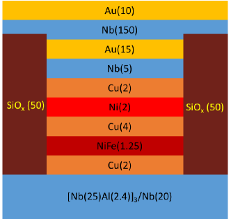
A cross-section of the Josephson junctions is shown in Figure 1. The SQUID devices were photolithographically patterned using a bilayer of LOR5B and S1813 photoresist. The bilayer gave a slight undercut in the resist after developing, which assists in liftoff by preventing metal on the sides of the deposited leads from sticking to the resist. A bottom [Nb/Al] superconducting base layer was used as previous work NiedzielskiThesis2017 ; Wang2012 has shown it has lower roughness than thick niobium, encouraging better growth of the ferromagnetic layers. The sputtered stack had the form [Nb(25)Al(2.4)]3/Nb(20)/Cu(2)/NiFe(1.25)/ Cu(4)/Ni(2)/Cu(2)/Nb(5)/Au(15) with all thicknesses in nanometers and subscripts indicating repeated layers. The gold capping layer was included to prevent oxidation. Previous work by our group on normal metal buffer layers NiedzielskiThesis2017 has shown that NiFe switches more sharply and at a lower field when grown on a copper buffer layer, so copper was sputtered between the superconducting and ferromagnetic layers. The Cu spacer was used to decouple the two ferromagnetic layers so they would switch independently. Sputtering was performed at a substrate temperature between and in an Ar pressure of in a system with a base pressure of . Permanent magnets were placed behind the substrates during sputtering to induce magnetocrystalline anisotropy along the long axis of the junctions. The Josephson junctions were then patterned by electron beam lithography using negative resist ma-N 2401. The stack was ion milled down to the niobium base layer, leaving the full stack only under the lithographically defined junctions. After ion milling, a insulating SiOx layer was thermally evaporated, followed by lift-off of the e-beam resist. The chips were pressed against a copper mass coated in silver paste for heatsinking during the ion milling and SiOx deposition. The top superconducting leads were photolithographically defined and the top Nb(150)/Au(10) superconducting electrode was sputtered.
III SQUID Design
Two patterns of SQUIDs, shown in Figure 2, were studied in this work. The first was a symmetric “pitchfork” design similar to the asymmetric design used in our previous work. The sample current is injected through the bottom lead, runs through the junctions in the SQUID, and returns via the top lead. The flux threading the SQUID is controlled by an independent current line on the chip running below the SQUID. In our previous phase-sensitive study, the difference in inductances between the two arms of the SQUID caused an asymmetry in the SQUID critical current oscillations which made it more difficult to identify the phase of the oscillation. A symmetric design is used here to simplify this stage of the analysis.
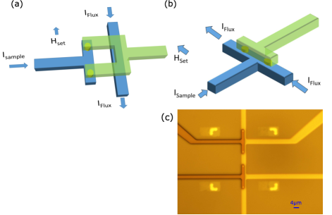
The second design studied is our “Ultra Low Inductance” (ULI) design shown in Figure 2(b). The sample current and flux current are injected via perpendicular wires on a common bottom electrode. An optical microscope image of this design taken before top-lead sputtering is shown in Figure 2(c). The junctions are patterned symmetrically with respect to the measurement current lead, and the top half of the SQUID lies directly above the flux line. This produces a SQUID loop with a cross-section perpendicular to the surface of the chip and a thickness governed only by the thickness of the thin insulating layer between the top and bottom leads. Because the junctions are placed symmetrically with respect to the bottom measurement current lead, the current through the sample couples no additional flux into the SQUID loop when the junction critical currents are equal. The flux current is provided using a Yokogawa current supply with a floating ground to minimize crosstalk between the measurement and flux currents. This design, as well as the pitchfork design, has the same nominal inductances for both arms. The lower inductances also reduce the relative shift between and that causes the distinctive “ratchet” shape in the SQUID oscillations seen in the asymmetric samples Gingrich2016 .
IV Measurement Procedure
The samples were initialized into the parallel magnetic state by applying a large (usually -4000 Oe) in-plane magnetic field to align both magnetic layers of both junctions in the negative direction. Although we are only able to measure the relative phase between the two junctions, we interpreted this state as having both junctions in the state based on the arguments outlined in the introduction. Switching the junctions one at a time would then sequentially bring the SQUID from the state to the and then states. After initialization, the chips were briefly raised above the surface of the helium in the cryostat to remove any trapped flux before measurement. IV curves were measured using a self-balancing SQUID-based potentiometer and battery-powered current supply. The flux current was provided by a programmable Yokogawa voltage source and a 1 k resistor. With no applied set field, IV curves were measured as the flux current was swept to identify the location of the central maximum of the SQUID oscillations in the state. The flux current range was selected to cover several lobes of the critical current oscillations, usually from to for the pitchforks. On the ULI samples, the magnetic field from the flux line suppressed the critical current in the junctions at large flux currents due to the Fraunhofer effect. Near zero field through the junction the critical current remains approximately constant, so we restricted the flux current to a narrow range from to . Above this range we saw a systematic decrease in critical current, which we attributed to this Fraunhofer suppression. All transport measurements were taken in zero field to ensure there was no suppression of the critical current from the set field.
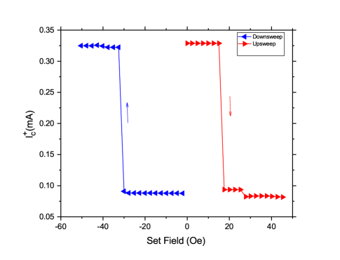
A preliminary measurement to identify the fields necessary to switch the first junction was performed by fixing the flux current at a maximum of the SQUID oscillation and sweeping the set field until a change in critical current is observed, as shown in Figure 3. The set field is then swept in the negative direction until the junction switches back. We observed a training effect where the switching field varies from run to run in early measurements, so this sweep is repeated until the switching characteristics stabilize from measurement to measurement. Once the constant-flux characteristics have been identified a full set of phase-sensitive measurements is performed. First, a small set field is applied in-plane. A series of IV curves is then measured in zero set field as the flux current is swept, giving several periods of the critical current oscillation vs flux. The set field is then incremented, and the process is repeated. Unless otherwise indicated the set field was incremented in steps of 5 Oe. When the first junction switches, an approximately half-period phase shift is observed in the raw data, indicating a switch of one junction from the to zero state. If the set field is further increased (a “major loop” measurement) the second junction switches, bringing the phase back to its original value. The set field was never brought above 100 Oe to avoid trapping flux in the devices.
Measurements were performed on SQUIDs on two chips. The first chip had three pitchfork samples, and the second contained four ULI SQUIDs. The large loop inductance of the pitchforks caused a relative shift between and , as seen in our previous work and described by theory. This offset caused a slanted “ratchet” shape in the SQUID oscillations which made it difficult to identify with certainty when a transition occurred. Nevertheless, the raw pitchfork data showed a change in the maximum critical current amplitude and a visible phase shift, suggesting that there was some form of switching occurring before extracting the shift in relative phase from a full analysis.
V Results
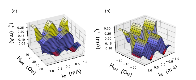
Figure 4 shows a 3D plot of critical current as a function of flux current and set field for a major loop measurement on an ultra-low inductance sample. Sweeping along the flux current axis shows the usual SQUID oscillation as a function of the flux coupled into the loop. As the set field is swept through the switching fields of the two junctions, the SQUID oscillations show a phase shift and a change in amplitude. Figure 4a shows the upsweep data for a ULI SQUID, with the set field being incremented in the positive direction from zero. When the set field reaches 20 Oe in the upsweep, the first junction switches. This is immediately evident in the raw data as the critical current oscillations shift by half a period. There is also a decrease in the maximum critical current as the critical current of these junctions is less in the antiparallel state than parallel. At 40 Oe, the second junction switches. This is again evident by inspection as there is another decrease in critical current and half-period shift. The downsweep data in Figure 4b, taken immediately after the upsweep, show the reverse process. At -20 Oe, there is an increase in critical current and half-period shift as the first junction returns to the parallel state. This is repeated at -60 Oe as the second junction switches to the parallel state. The clear half-period shifts make the changes between and states evident without further analysis.
Similar data is shown for a pitchfork SQUID in Figure 5. This measurement was a minor loop where the field was kept within a range that would only switch the first junction. The set field is incremented from zero in panel (a) until the first junction switches at 40 Oe. Again, a half-period shift is clearly observed. The set field is then incremented in the negative direction in panel (b) until the junction switches back at -40 Oe. Further changes in the critical current amplitude, but not phase, occur at -60 and -80 Oe, probably due to a domain wall being swept out of the NiFe free layer.
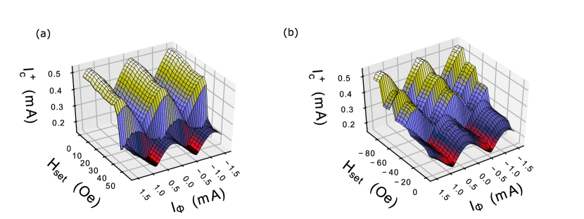
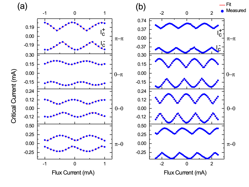
Figure 6 shows 2D plots of the critical current vs flux current for the two SQUID designs in the four possible magnetic states, as well as the fits to theory. Panel (a) shows and for an ultra-low inductance SQUID. The flux current is restricted to a narrow range on the ULI SQUIDs so that the field due to the flux line doesn’t significantly suppress the critical current by the Fraunhofer effect. Panel (b) shows similar data for a pitchfork SQUID. These data show that the maxima when the junctions are in the same state align with the minima when the junctions are in opposite states . As the critical current oscillation is periodic in the flux through the SQUID, a phase shift corresponds to a flux shift of in the oscillation. The theory fits the data very well and allows the extraction of the flux shift, inductances, and critical currents as described in section VI.
| Sample | State | (pH) | (pH) | (mA) | (mA) | |
|---|---|---|---|---|---|---|
| 1 | ||||||
| 2 | ||||||
| 3 | ||||||
| 1 | ||||||
| 4 | ||||||
Controllable switching was observed in all four of the ULI SQUIDS measured in this study. The average phase change for the ULI samples between the and states was . For the pitchforks the average phase change was . We attribute the difference in the pitchfork results to a slight flux being coupled into the SQUID by the NiFe nanomagnets as they switch. This issue is avoided in the ULI design due to their high symmetry.
| Sample | State | (pH) | (pH) | (mA) | (mA) | |
|---|---|---|---|---|---|---|
| 1 | 2 | |||||
| 2 | ||||||
| 3 | ||||||
VI Analysis
The standard model of a DC SQUID is characterized by four parameters: the inductances of the two arms and and the critical currents of the two junctions and . The inductance of the entire SQUID is characterized by the dimensionless parameter where is the loop inductance of the SQUID and is the sum of the critical currents of the two junctions SQUIDHandbookCh2 . The fits are described by the dimensionless parameters and which respectively characterize the asymmetries in the inductances and critical currents between arms. The fit also returns a value of for each SQUID oscillation. As the period of the oscillation corresponds to one flux quantum, a phase shift in one Josephson junctions induces a horizontal shift in the SQUID oscillation data by . The phase change was then calculated by taking the difference in between adjacent states. Because of the symmetric design, a preliminary fit was performed with the inductance asymmetry fixed at zero. The results of this fit were then used as initial guesses for a fit where all four parameters were allowed to vary. For all of the SQUIDs analyzed, the best fit supported half flux quantum shifts between adjacent states, as expected. In the four ULI SQUIDs studied, the fitting program always converged to the expected value of . For the pitchfork SQUIDs, it was possible to force the fit to converge to a value of differing from the expected value by half a flux quantum by allowing large inductance asymmetries and carefully choosing the initial guess, but the fit consistent with switching always had a lower . As noted in previous work Gingrich2016 , taking the wrong value for the phase shift also led to unphysical values for the inductances which changed from state to state. We are confident that the fits showing the shift incorporate the correct set of parameters for the pitchfork samples, and this issue was not observed in the ultra-low inductance samples.
Inductance simulations were performed in InductEx to compare to the values extracted from the fits for the two SQUID designs. The first round of simulations severely underestimated both the self and mutual inductances of the ULI SQUIDs. As described in section II, the bottom superconducting electrode consists of a Niobium/Aluminim multilayer instead of pure Niobium. In order for the simulations to acceptably match the experimental data, it was necessary to increase the London penetration depth of the Niobium/Aluminum layer from the conventional Niobium value of to . For the ULI SQUIDs, the average experimental self inductance (excluding the points that showed unphysically large inductance changes between states) was and a typical mutual inductance between the flux line and SQUID loop was , while the simulated values with were and . The experimental results for the pichforks gave and . Simulating this design with gave and . As a consistency check, we redid the simulations for our asymmetric SQUID study reported in Ref. Gingrich2016 with for the Niobium/Aluminum layer. The SQUID design in that study differed significantly in that the flux line ran alongside the loop several microns away instead of directly underneath it. Repeating the simulations of that SQUID did not show a significant change in the extracted inductance when was varied.
In our previous work, an increase in maximum critical current was observed as the junctions switched from the parallel to the antiparallel state. In choosing the Ni/NiFe thickness used for this study, the observations shown in Figure 3a of our single-junction results Niedzielski2018 were used to identify thicknesses where the critical current would be the same in the P and AP states. Those data suggested that for Ni(2.0), a NiFe(1.25) free layer should produce a junction with nearly equal critical currents in the P and AP states. Our data show that we in fact had a decrease in critical current as each junction switched into an AP state, and that in our full stack the thicknesses chosen were not exactly at the crossing point shown in the single-junction data. This characteristic decrease in critical current from the P to AP state is observed for both switches in every sample measured. Given the findings of our single-junction study and the fact that the critical currents we observe are higher in the P state than AP we expect increasing the NiFe thickness slightly would bring the critical currents in the two states closer together.
VII Conclusions
In conclusion, we have performed a comprehensive study of SQUIDs containing spin-valve Josephson junctions with a Ni hard layer and NiFe soft layer. switching has been observed in these SQUIDs, expanding the phase diagram of known Ni/NiFe thicknesses that support this phase change. This switching has been observed in multiple devices with different designs, showing the fabrication and measurement procedures are robust and repeatable. Introducing the ultra-low inductance SQUID design has greatly simplified analysis, since the phase shift can be directly observed in the raw data.
There is still an extensive amount of work that needs to be done for Ni/NiFe Josephson junctions to be viable for use in a commercial device. While the possibility of phase control is now well-established, there is room for significant improvement in both device design and magnetic characterizations. Over the course of this study the switching field for all of the devices changed significantly from run to run. Several junctions also switched in several steps, rather than the clean switch desired for a binary device. Better understanding the behavior of the ferromagnetic layers and optimizing their switching behavior remains a high priority for future work.
The amount of data on ferromagnetic layer combinations that can support switching is still very limited, with prior phase sensitive measurements having been done on Ni(1.2)/NiFe(1.5) Gingrich2016 and Ni(3.3)/NiFe(1.6) Dayton2018 . Single-junction measurements Niedzielski2018 suggest that for Ni(2.0), switching should be possible for a range of NiFe thicknesses from about to , which is consistent with the findings presented here, and that switching should be possible for Ni(1.6) with NiFe thicknesses between 1.0 and and . While this study on Ni(2.0)/NiFe(1.25) adds another data point to that phase diagram, there is a significant need for both theoretical advancements in modeling complex spin-valve junctions and broader experimental studies to allow for any sort of optimization of these devices.
These controllable pseudo-spin-valves are part of an increasingly diverse range of Josephson junctions with some form of phase control Yamashita2018 . This phase control has immediate application in multiple areas of superconducting electronics. A superconducting field-programmable gate array has been designed using magnetic Josephson junctions for using in single-flux-quantum (SFQ) computing Pedram2018 . junctions have applications in both high-speed low-power classical computing UstinovKaplunenko2003 ; Ortlepp2006 ; Khabipov2010 ; Kamiya2018 and in quantum computing Ioffe1999 ; Blatter2001 ; Yamashita2005 ; Feofanov2010 . The ability to control the phase state of a junction in-situ will surely lead to a wealth of new circuit designs.
Acknowledgements.
We are grateful to V. Aguilar for his assistance with measurement software and instrumentation. We are grateful to B.M. Niedzielski and J.A. Glick for their support with sample fabrication and measurement. We acknowledge valuable discussion with E.C. Gingrich, D. Miller, N.D. Rizzo, O. Naaman, D.S. Holmes, and A.Y. Herr. We also thank B. Bi for technical assistance and the use of the W.M. Keck Microfabrication Facility. This research is based upon work supported by the ODNI, IARPA, via ARO contract number W911NF-14-C-0115. The views and conclusions contained herein are those of the authors and should not be interpreted as necessarily representing the official policies or endorsements, either expressed or implied, of the ODNI, IARPA, or the U.S. Government.References
References
- [1] V. V. Ryazanov, V. A. Oboznov, A. Yu. Rusanov, A. V. Veretennikov, A. A. Golubov, and J. Aarts. Coupling of two superconductors through a ferromagnet: Evidence for a junction. Phys. Rev. Lett., 86:2427–2430, Mar 2001.
- [2] T. Kontos, M. Aprili, J. Lesueur, F. Genêt, B. Stephanidis, and R. Boursier. Josephson Junction through a Thin Ferromagnetic Layer: Negative Coupling. Phys. Rev. Lett., 89:137007, Sep 2002.
- [3] A. A. Golubov, M. Yu. Kupriyanov, and E. Il’ichev. The current-phase relation in Josephson junctions. Rev. Mod. Phys., 76:411–469, Apr 2004.
- [4] A. I. Buzdin. Proximity effects in superconductor-ferromagnet heterostructures. Rev. Mod. Phys., 77:935–976, Sep 2005.
- [5] E. A. Demler, G. B. Arnold, and M. R. Beasley. Superconducting proximity effects in magnetic metals. Phys. Rev. B, 55:15174–15182, Jun 1997.
- [6] A. I. Buzdin, L. N. Bulaevskii, and S. V. Panyukov. Critical-current oscillations as a function of the exchange field and thickness of the ferromagnetic metal (F) in an S-F-S Josephson junction. Pis’ma Zh. Eksp. Teor. Fiz., 35(4):147–148, 1982. [J. Exp. Theor. Phys. Lett., 35, 4, 20 (1982)].
- [7] A. I. Buzdin and M. Yu. and Kupriyanov. Josephson junction with a ferromagnetic layer. Pis’ma Zh. Eksp. Teor. Fiz., 53(6):308–312, 1991. [J. Exp. Theor. Phys. Lett., 53, 6, 321 (1991)].
- [8] F. S. Bergeret, A. F. Volkov, and K. B. Efetov. Enhancement of the Josephson current by an exchange field in superconductor-ferromagnet structures. Phys. Rev. Lett., 86:3140–3143, Apr 2001.
- [9] V. N. Krivoruchko and E. A. Koshina. From inversion to enhancement of the dc Josephson current in tunnel structures. Phys. Rev. B, 64:172511, Oct 2001.
- [10] A. A. Golubov, M. Yu. Kupriyanov, and Ya. V. Fominov. Critical current in SFIFS junctions. JETP Lett., 75:190–194, Feb 2002.
- [11] Yu. S. Barash, I. V. Bobkova, and T. Kopp. Josephson current in S-FIF-S junctions: Nonmonotonic dependence on misorientation angle. Phys. Rev. B, 66:140503, Oct 2002.
- [12] Ya. M. Blanter and F. W. J. Hekking. Supercurrent in long SFFS junctions with antiparallel domain configuration. Phys. Rev. B, 69:024525, Jan 2004.
- [13] Z. Pajović, M. Božović, Z. Radović, J. Cayssol, and A. Buzdin. Josephson coupling through ferromagnetic heterojunctions with noncollinear magnetizations. Phys. Rev. B, 74:184509, Nov 2006.
- [14] B. Crouzy, S. Tollis, and D. A. Ivanov. Josephson current in a superconductor-ferromagnet junction with two noncollinear magnetic domains. Phys. Rev. B, 75:054503, Feb 2007.
- [15] C. Bell, G. Burnell, C. W. Leung, E. J. Tarte, D.-J. Kang, and M. G. Blamire. Controllable Josephson current through a pseudospin-valve structure. Appl. Phys. Lett., 84(7):1153–1155, 2004.
- [16] A. F. Hebard and A. T. Fiory. A memory device utilizing the storage of Abrikosov vortices at an array of pinning sites in a superconducting film. AIP Conf. Proc., 44(1):465–469, 1978.
- [17] Shingo Uehara and Koichi Nagata. Trapped vortex memory cells. App. Phys. Lett., 39(12):992–993, 1981.
- [18] S. M. Faris, W. H. Henkels, E. A. Valsamakis, and H. H. Zappe. Basic design of a Josephson technology cache memory. IBM J. Res. Dev., 24(2):143–154, March 1980.
- [19] K. Miyahara, Y. Yamauchi, M. Yamamoto, and A. Ishida. An improved NDRO josephson quantized loop memory cell with buffering configuration. IEEE Trans. Electron Devices, 31(7):888–894, July 1984.
- [20] Kazunori Miyahara, Masashi Mukaida, and Kohji Hohkawa. Abrikosov vortex memory. Appl. Phys. Lett., 47(7):754–756, 1985.
- [21] S. Nagasawa, Y. Hashimoto, H. Numata, and S. Tahara. A 380 ps, 9.5 mW Josephson 4-Kbit RAM operated at a high bit yield. IEEE Trans. Appl. Supercond., 5(2):2447–2452, June 1995.
- [22] Valery V. Ryazanov, Vitaly V. Bol’ginov, Danila S. Sobanin, Igor V. Vernik, Sergey K. Tolpygo, Alan M. Kadin, and Oleg A. Mukhanov. Magnetic Josephson junction technology for digital and memory applications. Physics Procedia, 36:35 – 41, 2012.
- [23] Sangjun Oh, D. Youm, and M. R. Beasley. A superconductive magnetoresistive memory element using controlled exchange interaction. App. Phys. Lett., 71(16):2376–2378, 1997.
- [24] T. W. Clinton and Mark Johnson. Nonvolatile switchable Josephson junctions. Journal of Applied Physics, 85(3):1637–1643, 1999.
- [25] N. Yoshikawa, T. Tomida, M. Tokuda, Q. Liu, X. Meng, S. R. Whiteley, and T. Van Duzer. Characterization of 4 K CMOS devices and circuits for hybrid Josephson-CMOS systems. IEEE Trans. Appl. Supercond., 15(2):267–271, 2005.
- [26] R. Held, J. Xu, A. Schmehl, C. W. Schneider, J. Mannhart, and M. R. Beasley. Superconducting memory based on ferromagnetism. Appl. Phys. Lett., 89(16):163509, 2006.
- [27] I. V. Vernik, V. V. Bol’ginov, S. V. Bakurskiy, A. A. Golubov, M. Y. Kupriyanov, V. V. Ryazanov, and O. A. Mukhanov. Magnetic Josephson junctions with superconducting interlayer for cryogenic memory. IEEE Trans. Appl. Supercond., 23(3):1701208–1701208, June 2013.
- [28] E. Goldobin, H. Sickinger, M. Weides, N. Ruppelt, H. Kohlstedt, R. Kleiner, and D. Koelle. Memory cell based on a Josephson junction. Appl. Phys. Lett., 102(24):242602, 2013.
- [29] Junbo Park, G. E. Rowlands, O. J. Lee, D. C. Ralph, and R. A. Buhrman. Macrospin modeling of sub-ns pulse switching of perpendicularly magnetized free layer via spin-orbit torques for cryogenic memory applications. App. Phys. Lett., 105(10):102404, 2014.
- [30] I. I. Soloviev, N. V. Klenov, S. V. Bakurskiy, V. V. Bol’ginov, V. V. Ryazanov, M. Yu. Kupriyanov, and A. A. Golubov. Josephson magnetic rotary valve. Appl. Phys. Lett., 105(24):242601, 2014.
- [31] T. Golod, A. Iovan, and V. M. Krasnov. Single Abrikosov vortices as quantized information bits. Nature Communications, 6:8628, Oct 2015.
- [32] S. V. Bakurskiy, N. V. Klenov, I. I. Soloviev, M. Yu. Kupriyanov, and A. A. Golubov. Superconducting phase domains for memory applications. Appl. Phys. Lett., 108(4):042602, 2016.
- [33] J. B. Yau, Y. K. K. Fung, and G. W. Gibson. Hybrid cryogenic memory cells for superconducting computing applications. In 2017 IEEE International Conference on Rebooting Computing (ICRC), pages 1–3, Nov 2017.
- [34] S.V. Bakurskiy, N.V. Klenov, I.I. Soloviev, N.G. Pugach, M. Yu. Kupriyanov, and A.A Golubov. Protected states in SIsFS junctions for Josephson memory and logic. App. Phys. Lett., 2018. Accepted.
- [35] D. S. Holmes, A. L. Ripple, and M. A. Manheimer. Energy-efficient superconducting computing—power budgets and requirements. IEEE Trans. Appl. Supercond., 23:1701610, 2013.
- [36] I. I. Soloviev, N. V. Klenov, S. V. Bakurskiy, M. Yu. Kupriyanov, A. L. Gudkov, and A. S. Sidorenko. Beyond Moore’s technologies: operation principles of a superconductor alternative. Beilstein J. Nanotechnol., 8:2689, 2017.
- [37] B. Baek, W. H. Rippard, S. P. Benz, S. E. Russek, and P. D. Dresselhaus. Hybrid superconducting-magnetic memory device using competing order parameters. Nature Commun., 5:3888, 2014.
- [38] Makram Abd El Qader, R. K. Singh, Sarah N. Galvin, L. Yu, J. M. Rowell, and N. Newman. Switching at small magnetic fields in Josephson junctions fabricated with ferromagnetic barrier layers. Appl. Phys. Lett., 104(2):022602, 2014.
- [39] E. C. Gingrich, Bethany M. Niedzielski, Joseph A. Glick, Yixing Wang, D. L. Miller, Reza Loloee, W. P. Pratt Jr, and Norman O. Birge. Controllable 0- Josephson junctions containing a ferromagnetic spin valve. Nat. Phys., 12(6):564–567, Jun 2016.
- [40] Bethany M. Niedzielski, T. J. Bertus, Joseph A. Glick, R. Loloee, W. P. Pratt, and Norman O. Birge. Spin-valve Josephson junctions for cryogenic memory. Phys. Rev. B, 97:024517, Jan 2018.
- [41] I. M. Dayton, T. Sage, E. C. Gingrich, M. G. Loving, T. F. Ambrose, N. P. Siwak, S. Keebaugh, C. Kirby, D. L. Miller, A. Y. Herr, Q. P. Herr, and O. Naaman. Experimental demonstration of a Josephson magnetic memory cell with a programmable -junction. IEEE Magnetics Letters, 9:1–5, 2018.
- [42] B. Baek, M. L. Schneider, M. R. Pufall, and W. H. Rippard. Phase offsets in the critical-current oscillations of Josephson junctions based on Ni and Ni- barriers. Phys. Rev. Applied, 7:064013, Jun 2017.
- [43] S. M. Frolov, D. J. Van Harlingen, V. A. Oboznov, V. V. Bolginov, and V. V. Ryazanov. Measurement of the current-phase relation of superconductor/ferromagnet/superconductor Josephson junctions. Phys. Rev. B, 70:144505, Oct 2004.
- [44] J. J. A. Baselmans, A. F. Morpurgo, B. J. van Wees, and T. M. Klapwijk. Reversing the direction of the supercurrent in a controllable Josephson junction. Nature, 397:43, Jan 1999.
- [45] J. J. A. Baselmans, B. J. van Wees, and T. M. Klapwijk. Nonequilibrium supercurrent transport in controllable superconductor–normal-metal–superconductor junctions. Phys. Rev. B, 63:094504, Jan 2001.
- [46] Jian Huang, F. Pierre, Tero T. Heikkilä, Frank K. Wilhelm, and Norman O. Birge. Observation of a controllable junction in a 3-terminal Josephson device. Phys. Rev. B, 66:020507, Jul 2002.
- [47] Frank K. Wilhelm, Gerd Schön, and Andrei D. Zaikin. Mesoscopic superconducting–normal metal–superconducting transistor. Phys. Rev. Lett., 81:1682–1685, Aug 1998.
- [48] S.-K. Yip. Energy-resolved supercurrent between two superconductors. Phys. Rev. B, 58:5803–5807, Sep 1998.
- [49] S.-K. Yip. Magnetic-field effect on the supercurrent of an SNS junction. Phys. Rev. B, 62:R6127–R6130, Sep 2000.
- [50] T. T. Heikkilä, F. K. Wilhelm, and G. Schön. Non-equilibrium supercurrent through mesoscopic ferromagnetic weak links. EPL (Europhysics Letters), 51(4):434, 2000.
- [51] T. Yamashita, S. Takahashi, and S. Maekawa. Controllable junction with magnetic nanostructures. Phys. Rev. B, 73:144517, Apr 2006.
- [52] J-P Cleuziou, Wolfgang Wernsdorfer, V Bouchiat, Th Ondarçuhu, and M Monthioux. Carbon nanotube superconducting quantum interference device. Nat. Nanotech., 1(1):53–59, 2006.
- [53] R. Delagrange, R. Weil, A. Kasumov, M. Ferrier, H. Bouchiat, and R. Deblock. 0- quantum transition in a carbon nanotube Josephson junction: Universal phase dependence and orbital degeneracy. Physica B: Condensed Matter, 536:211 – 222, 2018.
- [54] Jorden A Van Dam, Yuli V Nazarov, Erik PAM Bakkers, Silvano De Franceschi, and Leo P Kouwenhoven. Supercurrent reversal in quantum dots. Nature, 442(7103):667, 2006.
- [55] D. B. Szombati, S. Nadj-Perge, D. Car, S. R. Plissard, E. P. A. M. Bakkers, and L. P. Kouwenhoven. Josephson -junction in nanowire quantum dots. Nature Physics, 12:568 – 572, May 2016.
- [56] Boris Kastening, Dirk K. Morr, Dirk Manske, and Karl Bennemann. Novel Josephson effect in triplet-superconductor–ferromagnet–triplet-superconductor junctions. Phys. Rev. Lett., 96:047009, Feb 2006.
- [57] Benjamin, C., Jonckheere, T., Zazunov, A., and Martin, T. Controllable junction in a Josephson quantum-dot device with molecular spin. Eur. Phys. J. B, 57(3):279–289, 2007.
- [58] Babak Zare Rameshti, Ali G. Moghaddam, and Malek Zareyan. Gate-controlled supercurrent reversal in MoS2-based Josephson junctions. EPL (Europhysics Letters), 108(3):37002, 2014.
- [59] S. Mironov, E. Goldobin, D. Koelle, R. Kleiner, Ph. Tamarat, B. Lounis, and A. Buzdin. Anomalous Josephson effect controlled by an Abrikosov vortex. Phys. Rev. B, 96:214515, Dec 2017.
- [60] Falko Pientka, Anna Keselman, Erez Berg, Amir Yacoby, Ady Stern, and Bertrand I. Halperin. Topological superconductivity in a planar Josephson junction. Phys. Rev. X, 7:021032, May 2017.
- [61] Bethany M. Niedzielski. Phase Sensitive Measurements of Ferromagnetic Josephson Junctions for Cryogenic Memory Applications. PhD thesis, Michigan State University, 2017.
- [62] Y. Wang, W. P. Pratt Jr, and N. O. Birge. Area-dependence of spin-triplet supercurrent in ferromagnetic Josephson junctions. Phys. Rev. B, 85:214522, 2012.
- [63] Boris Chesca, Reinhold Kleiner, and Dieter Koelle. SQUID Theory. In J. Clarke and A. I. Braginski, editors, The SQUID Handbook, chapter 2, pages 29–92. Wiley-Blackwell, 2005.
- [64] Taro Yamashita. Phase shift and control in superconducting hybrid structures. IEICE Transactions on Electronics, E101.C(5):378–384, 2018.
- [65] N. K. Katam, O. A. Mukhanov, and M. Pedram. Superconducting magnetic field programmable gate array. IEEE Trans. Appl. Supercond., 28(2):1–12, March 2018.
- [66] A. V. Ustinov and V. K. Kaplunenko. Rapid single-flux quantum logic using -shifters. J. App. Phys., 94(8):5405–5407, 2003.
- [67] T. Ortlepp, Ariando, O. Mielke, C. J. M. Verwijs, K. F. K. Foo, H. Rogalla, F. H. Uhlmann, and H. Hilgenkamp. Flip-flopping fractional flux quanta. Science, 312(5779):1495–1497, 2006.
- [68] M I Khabipov, D V Balashov, F Maibaum, A B Zorin, V A Oboznov, V V Bolginov, A N Rossolenko, and V V Ryazanov. A single flux quantum circuit with a ferromagnet-based Josephson -junction. Superconductor Science and Technology, 23(4):045032, 2010.
- [69] Tomohiro Kamiya, Masamitsu Tanaka, Kyosuke Sano, and Akira Fujimaki. Energy/space-efficient rapid single-flux-quantum circuits by using -shifted Josephson junctions. IEICE Transactions on Electronics, E101.C(5):385–390, 2018.
- [70] L. B. Ioffe, V. B. Geshkenbein, M. V. Feigel’man, A. L. Fauchere, and G. Blatter. Environmentally decoupled sds-wave Josephson junctions for quantum computing. Nature, 398:679–681, 1999.
- [71] G. Blatter, V. B. Geshkenbein, and L. B. Ioffe. Design aspects of superconducting-phase quantum bits. Phys. Rev. B, 63:174511, 2001.
- [72] T. Yamashita, K. Tanikawa, S. Takahashi, and S. Maekawa. Superconducting qubit with a ferromagnetic Josephson junction. Phys. Rev. Lett., 95:097001, 2005.
- [73] A. K. Feofanov, V. A. Oboznov, V. V. Bol’ginov, J. Lisenfeld, S. Poletto, V. V. Ryazanov, A. N. Rossolenko, M. Khabipov, D. Balashov, A. B. Zorin, P. N. Dmitriev, V. P. Koshelets, and A. V. Ustinov. Implementation of superconductor/ferromagnet/ superconductor -shifters in superconducting digital and quantum circuits. Nat. Phys., 6(8):593–597, Aug 2010.