Signatures of long-range-correlated disorder in the magnetotransport of ultrathin topological insulators
Abstract
In an ultrathin topological insulator (TI) film, a hybridization gap opens in the TI surface states, and the system is expected to become either a trivial insulator or a quantum spin Hall insulator when the chemical potential is within the hybridization gap. Here we show, however, that these insulating states are destroyed by the presence of a large and long-range-correlated disorder potential, which converts the expected insulator into a metal. We perform transport measurements in ultrathin, dual-gated topological insulator films as a function of temperature, gate voltage, and magnetic field, and we observe a metallic-like, non-quantized conductivity, which exhibits a weak antilocalization-like cusp at low magnetic field and gives way to a nonsaturating linear magnetoresistance at large field. We explain these results by considering the disordered network of electron- and hole-type puddles induced by charged impurities. We argue theoretically that such disorder can produce an insulator-to-metal transition as a function of increasing disorder strength, and we derive a condition on the band gap and the impurity concentration necessary to observe the insulating state. We also explain the linear magnetoresistance in terms of strong spatial fluctuations of the local conductivity, using both numerical simulations and a theoretical scaling argument.
I Introduction
Three-dimensional topological insulators (TIs) are an exotic state of matter in which gapless electronic excitations exist at the surface of a bulk system with gapped conduction and valence bands.Hsieh et al. (2009) These surface states exhibit a number of interesting phenomena associated with their linear dispersion and spin-momentum locking, Hasan and Kane (2010) including magnetic monopole responses to applied electric field Qi et al. (2009) and a strong magnetoelectric effect. Essin et al. (2009) Angle-resolved photoemission spectroscopy (ARPES) measurements have identified gapless Dirac surface states in several materials, including Bi1-xSbx, Bi2Se3, Sb2Te3, Bi2Te3. Hasan and Kane (2010)
When a TI crystal is made very thin, however, the nature of the surface states undergoes a significant change. In such ultrathin TI films, electrons have a finite amplitude for quantum tunneling between the top and bottom surfaces, resulting in a hybridization gap for the surface states whose magnitude depends on the film thickness . Under the right conditions, this gap can stabilize the quantum spin Hall state, which is characterized by one-dimensional, helical edge states around the border of the TI surface (as has been observed in the 2D TI HgTe/CdTe König et al. (2007); Roth et al. (2009)).
One can therefore expect a basic dichotomy of possibilities for an undoped, ultrathin TI film. Either the system becomes a trivial insulator, with a vanishing conductivity in the limit of zero temperature, or it becomes a quantum spin Hall insulator, with a quantized conductance. The fate of the TI film vis-a-vis these two possibilities is predicted to depend in a nontrivial way on the value of the thickness , with the system oscillating between a quantum spin Hall and a trivial insulating state as a function of thickness.Liu et al. (2010)
In this paper, however, we find evidence for a third possibility, outside of this dichotomy, in which a hybridization gap exists but the insulating state is destroyed by the presence of long-range-correlated disorder. We measure the resistivity of ultrathin films of pristine (Bi,Sb)2Te3 as a function of temperature, chemical potential, and magnetic field, and we find a number of features that suggest that a dominant role is played by long-range-correlated disorder, which arises inevitably due to charged impurities in the film and in the substrate. Our films are 4 quintuple layers (QLs) thick, which is predicted to produce a quantum spin Hall insulator, but we find instead a finite, nonquantized value of the resistance in the limit of zero temperature. We provide an explanation for this observation in terms of an insulator-to-metal transition produced by increasing long-ranged disorder. We also observe a prominent weak anti-localization correction and a large linear magnetoresistance at high magnetic fields, which we explain in terms of strong spatial fluctuations of the local conductivity.
The remainder of this paper is organized as follows. In Sec. II we briefly describe our sample preparation and measurement setup. Section III describes our zero-field measurements, and presents theoretical arguments to explain a resistivity that is both finite and non-quantized in the limit of zero temperature. Section IV presents results for the resistivity as a function of magnetic field and gate voltage, along with a theoretical discussion of both the weak antilocalization corrections and the linear magnetoresistance that we observe.
II Sample preparation and measurement setup
Our TI films are made from 4 QLs of (Bi,Sb)2Te3 grown on a SrTiO3(111) substrate using molecular-beam epitaxy in an ultra-high vacuum. Each QL layer is nm thick. The Bi, Sb and Te effusion cells as well as the SrTiO3 (111) substrate are held at high temperature in order to ensure precise control of surface stoichiometry. The crystallinity of the films is monitored by reflection high-energy electron diffraction (RHEED) pattern. To prevent oxidation in ambient conditions, nm of Tellurium and nm of Alumina capping layer is grown on top of the films. The samples tend to degrade at high temperatures, and hence all the processing was done at no higher than 100 ∘C. Contacts were made using e-beam lithography. In the dual gated devices, the top gate dielectric was made from 20 nm of HfO2 grown by atomic layer deposition.Nandi et al. (2018) Magneto-transport measurements are performed in a dilution refrigerator with a 8 T magnet and using low frequency ac lockin techniques. Results in this paper are taken from five Hall bar devices, which we denote H1, H2, H3, H4 and H5 .
III Transport at zero magnetic field
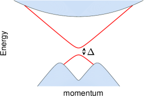
As mentioned in the Introduction, hybridization between the two parallel TI surfaces leads to a gap opening at the Dirac point of the surface dispersion relation (as illustrated in Fig. 1). The size of this gap is generally expected to be between 5 meV and 50 meV; this range encompasses estimates from density functional theory and tight-binding models for the gaps in 4-QL-thick Bi2Se3 and Bi2Te3.Liu et al. (2010) For situations where the chemical potential resides in the middle of the gap and there is no band bending, one would expect the TI surface to become an insulator with an activation energy for the conductivity. Such a state would have either zero conductivity in the limit of zero temperature (if the system is a trivial insulator) or a quantized conductance (if the system forms a quantum spin Hall state).
Using a dual-gated FET setup, we shift the chemical potential for both the top and bottom surfaces of our samples across a wide range in order to search for these insulating states. At large negative voltages the chemical potential resides far below the energy of the Dirac point, while at large positive voltages the chemical potential is high above. When the two gate voltages are chosen such that both surfaces are at the charge-neutral point (CNP), the system assumes its maximally insulating state. This behavior is shown in Fig. 2 for five different samples as a function of the back gate voltage. (The behavior as a function of both back and top gate voltages is discussed in the Supplementary Material.)
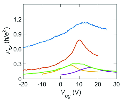
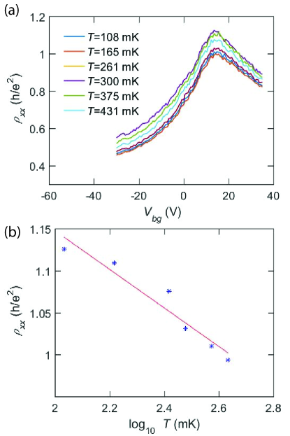
Contrary to the expectation for a clean system, our measurements reveal a conductivity that is neither insulating-like nor quantized. Indeed, Fig. 2 shows that the resistance takes a value of order at the CNP, but this value varies from one sample to the next. As shown in Fig. 3, the resistivity depends very weakly on temperature, even though the temperature is far below K. Using the traditional description of an undoped semiconductor, one would predict an activated dependence .
Taken together, these two observations suggest that the system is not well described by either the clean band insulator or quantum spin Hall insulator states. The most trivial explanation for our results would be that the surface bands simply do not have a band gap. For example, in 4-QL-thick films of Bi2Te3 the point lies at a local minimum of the valence band, Yazyev et al. (2010) and consequently there is no finite window of energy with zero density of states. In Sb2Te3, tunneling experiments have shown that films of the same thickness have a thermodynamic gap that is no larger than a few meV. Jiang et al. (2012) Still, it is worth considering whether there is another, more interesting explanation for the lack of insulating behavior, especially since similar results have been recorded for transport in thin films of Bi2Se3, Kim et al. (2011) despite a Dirac point that lies well outside the bulk valence band states and a gap on the order of tens of meV. Liu et al. (2010); Zhang et al. (2010)
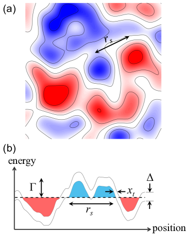
The apparent breakdown of the clean insulator picture can be rationalized by considering the effects of long-ranged disorder induced by Coulomb impurities, which exist both in the TI film and in the substrate. Such impurities are known to provide long-wavelength fluctuations of the local Fermi energy, which provide a finite density of states at zero energy due to band-bending. Skinner et al. (2013) This random band-bending effect is illustrated in Fig. 4. When the surface gap is sufficiently large, the fluctuations of the Fermi energy lead to the formation of isolated electron and hole puddles [red and blue regions of Fig. 4(a), respectively], separated by insulating tunnel barriers (white regions). When the chemical potential is precisely in the middle of the band gap (which we define as ), electron and hole puddles appear in equal number. Similar picture of fluctuating Fermi energy in the presence of insulating gap has been also adopted in graphene nanoribbons Stampfer et al. (2009) and dual-gated bilayer graphene Lee et al. (2015a). One can estimate the condition for maintaining a good insulating state at by demanding that the typical tunneling action for electron tunneling across such a barrier satisfy .
To estimate the action , we first assume that the typical magnitude of the disorder potential is sufficiently large that . We also assume that the typical correlation length of the potential is much larger than the film thickness. Both of these assumptions are validated below. Under these assumptions one can use numerical estimates for and based on a gapless TI surface. Skinner et al. (2014), 111The theoretical estimates of Ref. Skinner et al., 2014 are slightly modified for our case, since the two opposite TI surfaces screen the disorder in tandem and therefore the density of states should be doubled relative to the case of a single surface. These estimates give
| (1) |
and
| (2) |
where is the (three-dimensional) concentration of impurities in the TI film and substrate, is the reduced Planck constant, is the Dirac velocity, and is the effective fine structure constant, with the effective dielectric constant and the vacuum permittivity. If one assumes an impurity concentration of order cm-3, a Dirac velocity of order m/s, and an effective dielectric constant as large as several hundred (due to the close proximity of the highly-polarizable SrTiO3 substrate), then is of order , the disorder potential is of order meV, and nm. It is worth noting that at chemical potentials far from the CNP, both and will generally be smaller than their values.
In order to estimate the width of the typical spatial separation between electron and hole puddles, one can notice that the typical in-plane electric field is , so that is given by . Solving for and substituting Eqs. (1) and (2) gives . The typical tunneling action between electron and hole puddles can be estimated as the product of the height of the tunnel barrier and the time needed to traverse it. So . For the system to be insulating, one must have , which is equivalent to
| (3) |
Equation (3) can be viewed as a generic requirement for the existence of an insulating state in a gapped 2D system on a substrate with charged impurities. That is, either the gap must be large enough or the impurity concentration must be small enough that Eq. (3) is satisfied.
In our samples, the right-hand side of Eq. (3) is of order meV. For much smaller values of the gap, one can say that electron and hole puddles are well-connected by quantum tunneling, and there is no meaningful “insulating barrier” between them. Our samples apparently correspond to such a situation, where Eq. (3) is violated, so that one can think of the surface as effectively ungapped even though is finite. Producing a well-insulating TI thin film apparently requires either a larger hybridization gap or a much smaller impurity concentration . For the remainder of this paper we set when discussing transport.
The zero-field DC resistivity is given by , where is the typical Fermi wave vector and is the electron mean free path. For the “puddled” scenario depicted in Fig. 4, the typical value of at zero chemical potential is , while the mean free path is of the same order as . Thus, the resistivity at zero chemical potential is given by Skinner et al. (2014)
| (4) |
For our samples, this expression gives a value of order .
Our picture of conduction through a spatially-disordered landscape is also consistent with measurements of the superconducting proximity effect, which we present in the Supplementary Material.
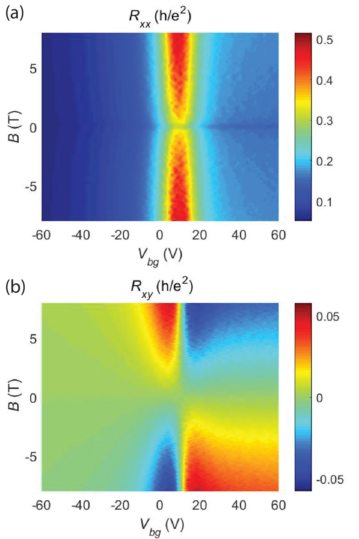
IV Magnetotransport
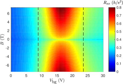
We also study the electron transport under the application of a perpendicular magnetic field. The measured longitudinal resistance is plotted in Fig. 5 for device H4 as a function of the field strength and the back gate voltage . For a given magnetic field, the resistance is maximized near the CNP, which for this device corresponds to V. The resistance also increases monotonically as a function of . In general, we observe an asymmetry between positive and negative voltages relative to the CNP, with negative voltages generally corresponding to smaller resistance. This asymmetry suggests that negative values of the chemical potential correspond to a larger density of states than positive values of the chemical potential, which may arise either because of curvature of the Dirac band or because of proximity of the Dirac point to the bulk valence band states (as depicted in Fig. 1). In our measurement conditions, the Hall resistance is everywhere much smaller than the longitudinal resistance ; this is shown explicitly in the Supplementary Material. Thus we can approximate the conductivity , where is the aspect ratio of the sample H5. The leading order correction to this expression is of order , which is smaller than throughout the regime of our measurements.
Our data show two notable features as a function of magnetic field. For any given gate voltage there is a sharp cusp in near , which previous experimental studies have attributed to weak antilocalization (WAL).Steinberg et al. (2011); Liu et al. (2012); Tian et al. (2014); Zhang et al. (2013); Kim et al. (2011) The correction to the conductivity associated with WAL is described by the theory of Hikami, Larkin, and Nagaoka: Hikami et al. (1980)
| (5) |
Here is the digamma function, is the phase coherence length, and is a numerical coefficient defined so that indicates WAL and corresponds to weak localization. The quantity is usually associated with the number of parallel conduction channels.
In Fig. 6 we plot as a function of magnetic field for different values of the back gate voltage. The sharp, logarithmic cusp of is consistent with Eq. (5), and we can perform good fits in the range in order to extract the parameters and . Interestingly, for low enough voltages that the chemical potential is far below the CNP, we find that all measured curves are identical, irrespective of the gate voltage [Fig. 6(a)]. Similarly, all measured values of for voltages far above the CNP also collapse onto a single curve [Fig. 6(c)], although this curve is distinct from the one corresponding to low voltages. In the intermediate voltage range (between the two dashed vertical lines in Fig. 6), the behavior of transitions smoothly from one limiting curve to the other [Fig. 6(b)]. We interpret these two limiting curves as corresponding to chemical potentials either far below or far above the Dirac point. In the latter case, the current is carried only by the linear Dirac surface states above the gap. In the opposite limit of small , the current moves through an admixture of Dirac surface states and conduction band states. For intermediate voltages, the disorder potential mixes these two behaviors spatially by random band bending.
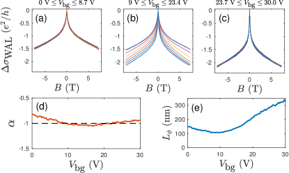
By fitting our data to Eq. (5), we are able to extract estimates for the constant and the phase coherence length as a function of the back gate voltage. These results are shown in Fig. 6(d) and (e), respectively. It is worth remarking that the inferred value of is everywhere close to , as one might expect for a conduction process with two parallel channels (arising from the two parallel surfaces). The estimated phase coherence length is on the order of several hundred nm, consistent with previous studies at low temperature.Steinberg et al. (2011); Tian et al. (2014)
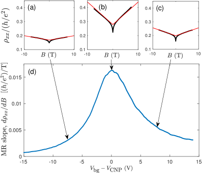
At larger magnetic field, the WAL correction gives way to a resistance that increases linearly with magnetic field strength, with no evidence of saturation. As shown in Fig. 7, this linear magnetoresistance (LMR) effect is most prominent near the CNP. As the chemical potential is moved away from the CNP in either direction, the slope of the LMR is reduced.
Multiple explanations have been proposed during the last few decades for nonsaturating LMR in 2D electron systems. For example, Wang and Lei have proposed a mechanism for LMR on a TI surface based on Zeeman splitting.Wang and Lei (2012) However, the magnitude of the LMR associated with this mechanism is much smaller than the value we observe. Indeed, to explain our largest observed LMR slope with the Zeeman splitting mechanism would apparently require an electron -factor of several hundred, which seems inconsistent with transport experiments in a tilted magnetic field. Chen et al. (2011) Other authors have explored more generic, semiclassical explanations for LMR, and have shown how it can arise from either persistent gradients of electron density Ilan et al. (2006) or mesoscopic spatial fluctuations of the mobility. Parish and Littlewood (2005); Kozlova et al. (2012) Such fluctuations are commonly treated using either resistor network models Parish and Littlewood (2005) or effective medium approaches Knap et al. (2014); Ping et al. (2014), which give largely equivalent results. Ramakrishnan et al. (2017)
Similar to these latter approaches, we suggest a way to understand our results based on a simple model in which the system is described by a local, Drude-like conductivity tensor that varies as a function of position due to spatial fluctuations in the electron density. In particular, we suppose that one can define local longitudinal and Hall conductivities and , respectively, which vary as a function of position . Such a description is generally valid so long as variations in the electron density occur over a length scale that is much longer than the mean free path or the Fermi wavelength .
In the Drude model, the ratio , where is the cyclotron frequency and is the transport scattering time. For a gapless Dirac system
| (6) |
where is the local value of the Fermi momentum and is the local mean free path. (As declared above, we are again ignoring the effects of any small band gap .) Note that the ratio becomes large when is sufficiently large. The value of the local Fermi momentum can be described by the Thomas-Fermi equation,
| (7) |
where is the Fermi energy relative to the Dirac point and is the electrostatic potential.
In order to understand the appearance of LMR within this model, consider first the case when the system is close enough to the CNP that electron and hole puddles exist in almost equal number, . This is the regime where the LMR is observed to be most prominent experimentally, and one can understand its appearance using the following scaling arguments. Near the CNP, electron and hole puddles are nearly equally abundant, and the local conductivity at the boundary between puddles is small because of the locally vanishing value of the electron density. Consequently, the current across the system is forced to pass through narrow “pinch points” of the random potential, where the electric potential is close to zero and adjacent electron- or hole-type puddles are narrowly separated. These pinch points provide the bottleneck for conduction, and they become more prominent with increasing magnetic field. Ruzin (1993) (See the Supplementary Material for simulated images of current flow.) One can think that an order unity number of such pinch points exist per square area , and consequently, if is the typical conductance of the pinch point, then the longitudinal resistivity of the system is .
To estimate the typical conductance of the pinch point, one can exploit the result for the (two-terminal) conductance of a square with nonzero Hall conductivityHans and Friedrich (1958); Jensen and Smith (1972); Abanin and Levitov (2008): . If the magnetic field is large enough, then at the pinch point and we arrive at the relation , where represents the Hall conductivity at the pinch point. At the Hall conductivity , and so our result for the longitudinal resistivity is equivalent to
| (8) |
where represents the typical Fermi momentum at the pinch point.
In general, pinch points are locations where the random potential is close to zero. Thus, if the chemical potential is not too close to zero, then Eq. (7) implies . As the chemical potential is shifted away from the CNP, the corresponding value of increases and the slope of the magnetoresistance declines. This is consistent with the experimental result in Fig. 7. On the other hand, as one approaches the CNP very closely, both the typical spatial size of the pinch point and its typical Fermi momentum are reduced, and the resistance increases. While the relation implies a divergence of the resistance at , such a divergence may be truncated by the finite mean free path. In other words, since the local conductivity is not well-defined at scales shorter than the mean free path , one can think that the minimal size of the pinch point is , and consequently that the minimal value of is , where is the typical value of near the center of an electron or hole puddle. Using the estimates for and presented below, and inserting the expression for into Eq. (8), gives a maximum magnetoresistance slope of order per Tesla of field. This is consistent in order of magnitude with our measured result.
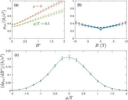
In order to test our scaling arguments quantitatively, we implemented numeric, finite-element simulations of current flow through a Hall bar geometry with a correlated disorder potential and a Drude-like conductivity tensor having a local value of given by Eq. (7). For simplicity, our simulations assume a transport scattering time that is independent of energy or position. While there is no reason a priori to expect this assumption to be accurate quantitatively, the scaling argument leading to Eq. (8) suggests that the longitudinal resistivity becomes independent of at sufficiently large field. As shown in Fig. 8, the simulation consistently reproduces the LMR trend, as well as the decline in the LMR slope with increasing chemical potential. Details of the simulation method are provided in the Supplementary Material (along with results for , which are consistent with experiment). Within the assumption of a constant scattering time, one can fit the experimental data at the CNP quantitatively by setting the root-mean-square Fermi momentum nm-1, and the mean free path nm. More details about the fitting are provided in the Supplementary Material.
V Conclusion
In this paper we have presented experimental results for the resistivity of thin TI films as a function of temperature, chemical potential, and magnetic field. In the absence of disorder, these systems are predicted to form a quantum spin Hall state. We find, however, that the transport in our system is dominated by long-range fluctuations of the disorder potential, presumably induced by charged impurities in the film and in the substrate. In particular, such long-ranged disorder creates a random landscape of - and -type regions, and this landscape destroys the insulating state. Our theoretical arguments suggest that one may reach an insulating state only when the gap is large enough and the impurity concentration is low enough that Eq. (3) is satisfied.
The magnetotransport shows signs of both weak antilocalization and a nonsaturating linear magnetoresistance. The WAL correction is described well by the usual Hikami-Larkin-Nagaoka theory, Eq. (5), with two parallel conduction channels (). We also find that collapses onto one of two curves when the chemical potential is far from the CNP. We have shown that the linear magnetoresistance can be interpreted as the result of spatial fluctuations in the local conductivity arising from strong disorder fluctuations. Our estimate of the linear MR slope and its dependence on chemical potential are both consistent with observations.
Taken together, our results provide new understanding of electron transport in ultrathin topological insulators, and may bring us closer to realizing ideal quantum spin Hall insulators. More broadly, our improved understanding of the disorder-induced insulator-to-metal transition and LMR may be important for a wide class of disordered 2D electron systems.
Acknowledgements.
It is a pleasure to thank I. Sodemann, A. Nahum, S. Simon, J. T. Chalker, A. Kamenev, and Y. P. Chen for valuable discussions. We are indebted to Di Wei, Lucas Orona, Tony Zhou, Charlotte Bøttcher, Michael Kosowsky and Andrew Pierce for invaluable help with fabrication and measurements. AY, DN, KS and JW acknowledge the support from Gordon and Betty Moore Foundation Grant No. 4531, NSF grant No. DMR-1708688, ARO Grant No. W911NF16-1-0491, ARO Grant No. W911NF-17-1-0023, and ARO grant No. W911NF-18-1-0316. Fabrication for this work was supported by DOE Award Number DE-SC0001819. BS was supported as part of the MIT Center for Excitonics, an Energy Frontier Research Center funded by the U.S. Department of Energy, Office of Science, Basic Energy Sciences under Award No. DE-SC0001088. BIH acknowledges support from the STC Center for Integrated Quantum Materials under NSF grant DMR-1231319. PK, GHL and KH acknowledge support from NSF Grant No. DMR-1420634. JSM, CZC and YO acknowledge the support from NSF Grant No. DMR-1700137, ONR Grant No. N00014-16-1-2657 and the Center for Integrated Quantum Materials under NSF Grant No. DMR-1231319. CZC also thanks the support from Alfred P. Sloan Research Fellowship and ARO Young Investigator Program Award (W911NF1810198).VI Supplemental Material for ‘Signatures of long-range-correlated disorder in the magnetotransport of ultrathin topological insulators’
VI.1 Hall measurements
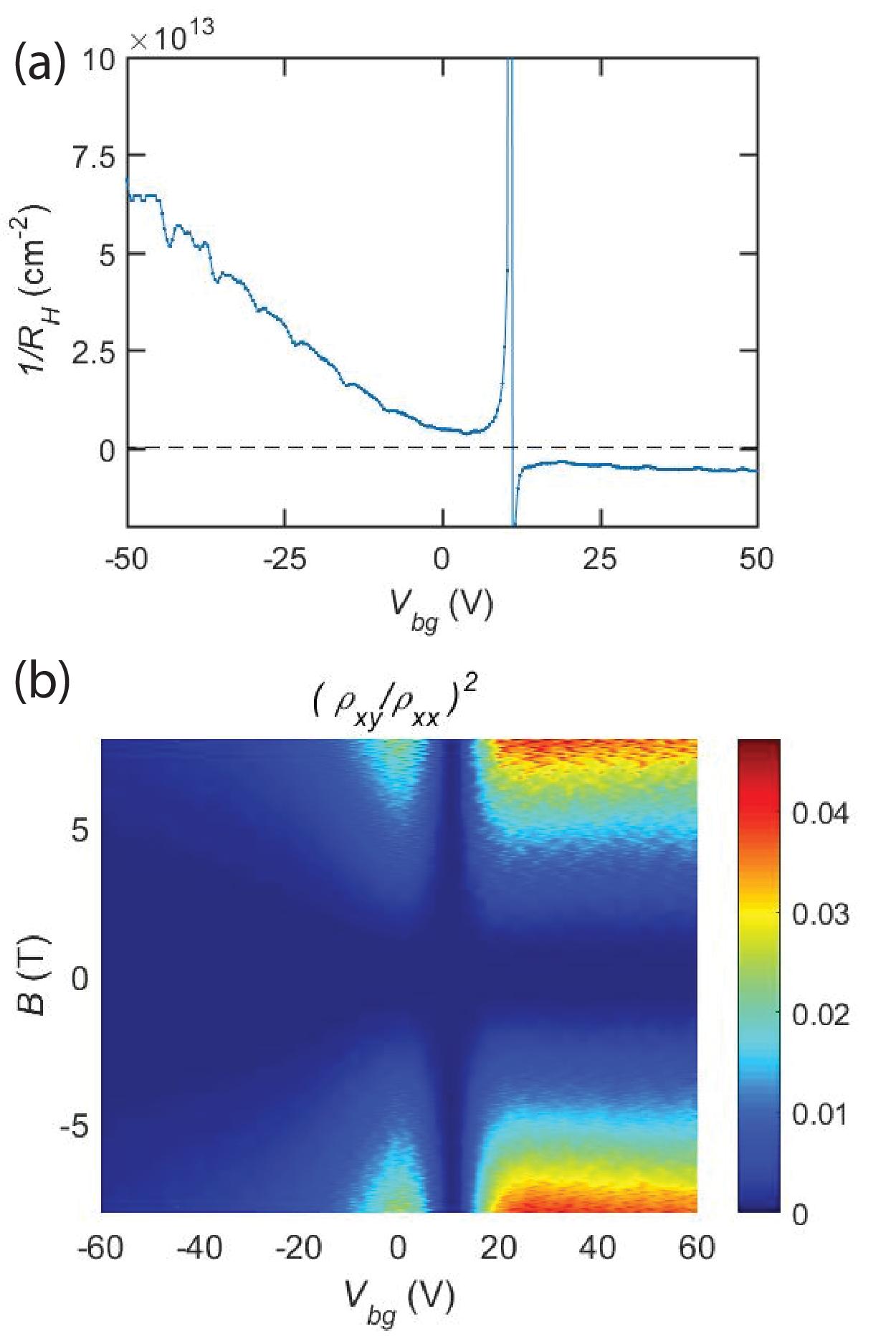
In the main text we focused on the longitudinal resistance and ignored the transverse Hall resistance . Here we present results for , and we show that it is everywhere much smaller than . In Fig. 9 we plot and for device H3 as a function of back gate voltage and magnetic field strength .
From the data, we calculate the inverse Hall coefficient , as shown in Fig. 10(a). The strong asymmetry in on different sides of the charge neutral point (CNP) reflects an asymmetry in the band structure of the TI films. The minimum value of cm-2 suggests a typical carrier density of electron and hole puddles. Similar results for were seen in Ref. Lee et al., 2015b.
In the presence of a perpendicular magnetic field, the conductivity is given in general by
| (9) |
Figure 10(b) shows that for all relevant magnetic field and backgate voltages, the quantity . Hence, the global conductivity can be well approximated by .
VI.2 Dual Gating
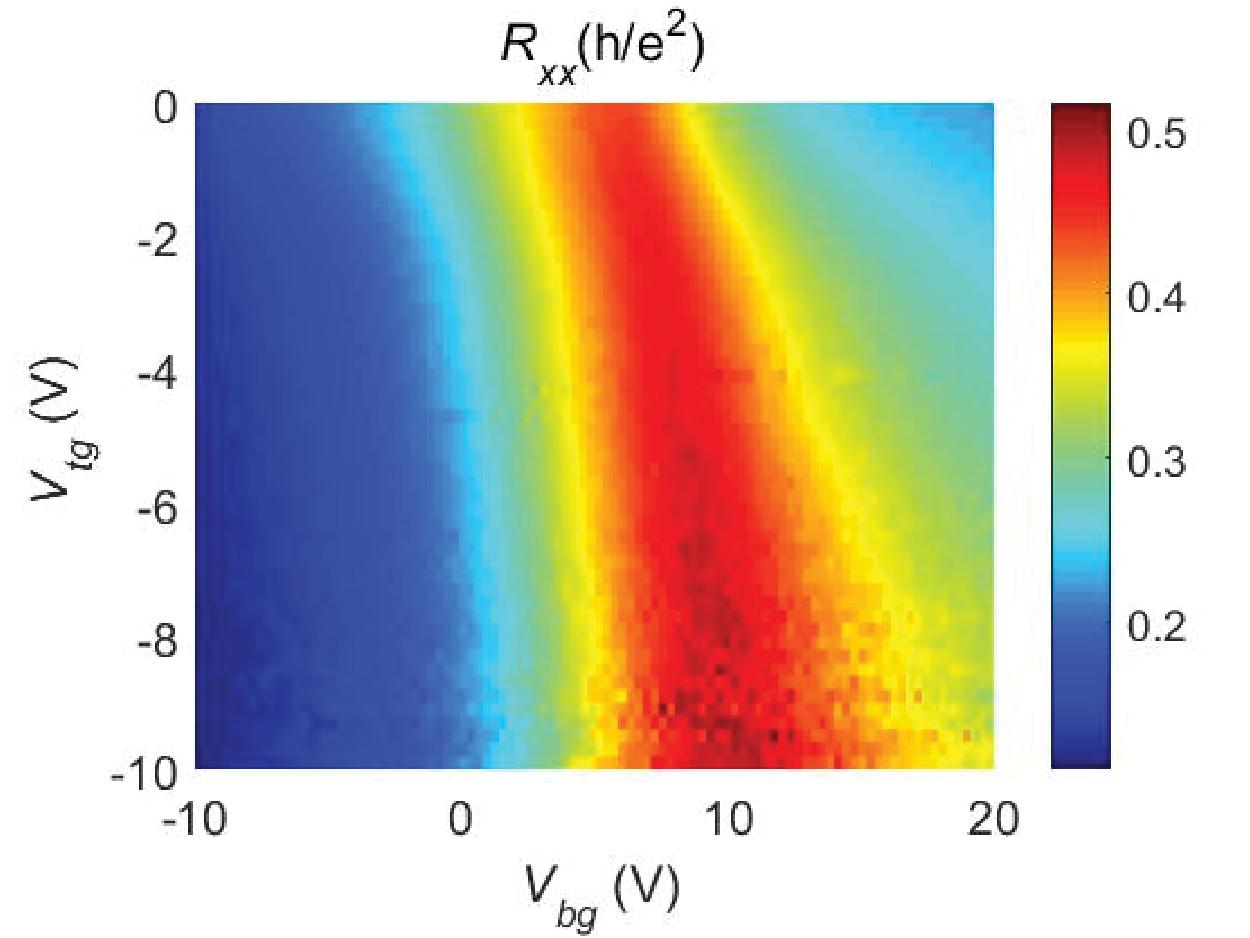
In some of our samples, both a back gate and a top gate were fabricated, allowing the chemical potential to be modulated by two independent gate voltages. In Fig. 11 we present the low-temperature longitudinal resistance for sample H4 as a function of the top and back gate voltages, and , respectively. For this sample, the longitudinal resistance exhibits a maximum of at the CNP, and there is no sign of an insulating state with large resistance.
VI.3 Superconducting proximity effect
Coupling superconductivity to topological insulator (TI) surface states is predicted to create a px+ipy superconductor with Majorana bound states.Fu and Kane (2008, 2008); Tanaka et al. (2009); Potter and Fu (2013) Such Majorana states may enable topologically protected qubits for quantum computation,Moore (2010) and consequently there has been an intensive search for Majorana modes in exfoliated 3D TIs Williams et al. (2012); Rokhinson et al. ; Kurter et al. (2015). Achieving Josephson coupling is an important step towards engineering topological superconductivity.
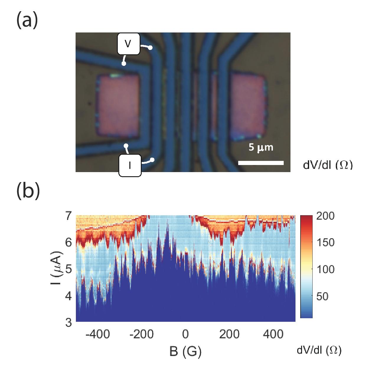
We investigated superconducting Josephson coupling mediated by the TI thin film, as depicted schematically in Fig. 12(a). An important consideration for achieving Josephson coupling is a transparent superconducting contact with minimum contact resistance. To make transparent contacts, we etched Tellurium capping layer covering topological insulator film (Bi,Sb)2Te3, and in-situ evaporated Ti (5 nm) / Nb (2.5 nm)/ NbN (50 nm) without breaking vacuum in the evaporation chamber. The device dimensions were 6 m 0.1 m, as shown in Fig. 12(b).
The interference pattern of the critical current () of the Josephson junction under perpendicular magnetic field gives valuable information about the Josephson current density () along the junction width. In the case of a spatially uniform Josephson current density, the interference pattern corresponds to a single slit Fraunhofer pattern where the lobes of decays with . On the other hand, for TIs in which conduction occurs dominantly at the edges of the system, the interference pattern is expected to resemble the double slit-like diffraction pattern of a dc SQUID with non-decaying lobes. In this case the critical current is given by
| (10) |
where is the magnetic flux quantum and is the area of the junction. Similar analyses of the interference pattern of Josephson junctions has shown edge dominant conduction in HgTe/HgCdTe 2D topological insulator Hart et al. (2014) and Bi1.5Sb0.5Te1.7Se1.3 3D TIs. Lee et al. (2014)
In our devices, the normal junction resistance and the maximum Josephson current A at the temperature of 50 mK give eV, which corresponds to about , where is the superconducting gap. The Josephson junction displays an interference pattern, as shown in Fig. 12(c), that cannot be explained by a uniform Josephson current distribution. The extracted period of the quasi-periodic oscillation of is about 35 G, which matches well with the expected value of G. Imperfect constructive and destructive interferences visible in the pattern are indicative of the effect of random disorder in the junction. Proximity-induced Josephson coupling and the similar interference pattern were also observed by us in Josephson junctions made of Ti (5 nm)/Al (50 nm).
VI.4 Numeric simulations of current flow
In the main text we presented results for the magnetoresistance based on a model where the local conductivity tensor varies with the position due to spatial variations in the electron/hole concentration. Here we present more details about our numeric simulations of the resistivity.
Within the Drude model, the conductivity tensor has the form
| (11) |
where the values of and are related to the value of the local electrostatic potential by
| (12) |
where is the local value of the Fermi momentum, is the local value of the cyclotron frequency, is the transport scattering time and is the mean free path. In principle, both and may have a dependency on the local Fermi energy, and therefore on position. However, for simplicity in our numeric simulations we take and to be constants with no spatial variation. The local Fermi momentum is related to the disorder potential by the Thomas-Fermi equation, Eq. (7) of the main text.
In order to address the problem computationally, we define the following dimensionless units. First, we define a normalized electrochemical potential
| (13) |
so that has a standard deviation of unity. Here, is the chemical potential and is the root-mean-square value of the disorder potential. The local value of the Fermi momentum is then given by
| (14) |
where represents the root-mean-square value of the Fermi momentum at zero chemical potential.
We also define a dimensionless magnetic field strength
| (15) |
where is the magnetic length. With these definitions, , and we can rewrite the elements of the conductivity tensor in dimensionless form as
| (16) |
Written in this form, the system is characterized by three dimensionless parameters: , , and . For a given choice of these parameters, and for a given realization of the random potential , one can solve for the current density through the system by solving the continuity equation
| (17) |
where , and is the local deviation of the electrochemical potential away from equilibrium. Below we present results based on a finite element solution to Eq. (17). For definiteness, we choose our simulated system to be a Hall bar with length and width , where is the correlation length of the potential (equivalent to in the main text). Applying a unit voltage across the long end of the bar gives the boundary conditions , , and . The finite-element mesh size was .
The random potential was taken to be a Fourier series with random coefficients whose magnitude decreases at high wave vector. Specifically, we write
| (18) |
where are random coefficients and
| (19) |
The coefficients are chosen to have a random phase in the complex plane and a random magnitude bounded by
| (20) |
The normalization of the potential is such that and .
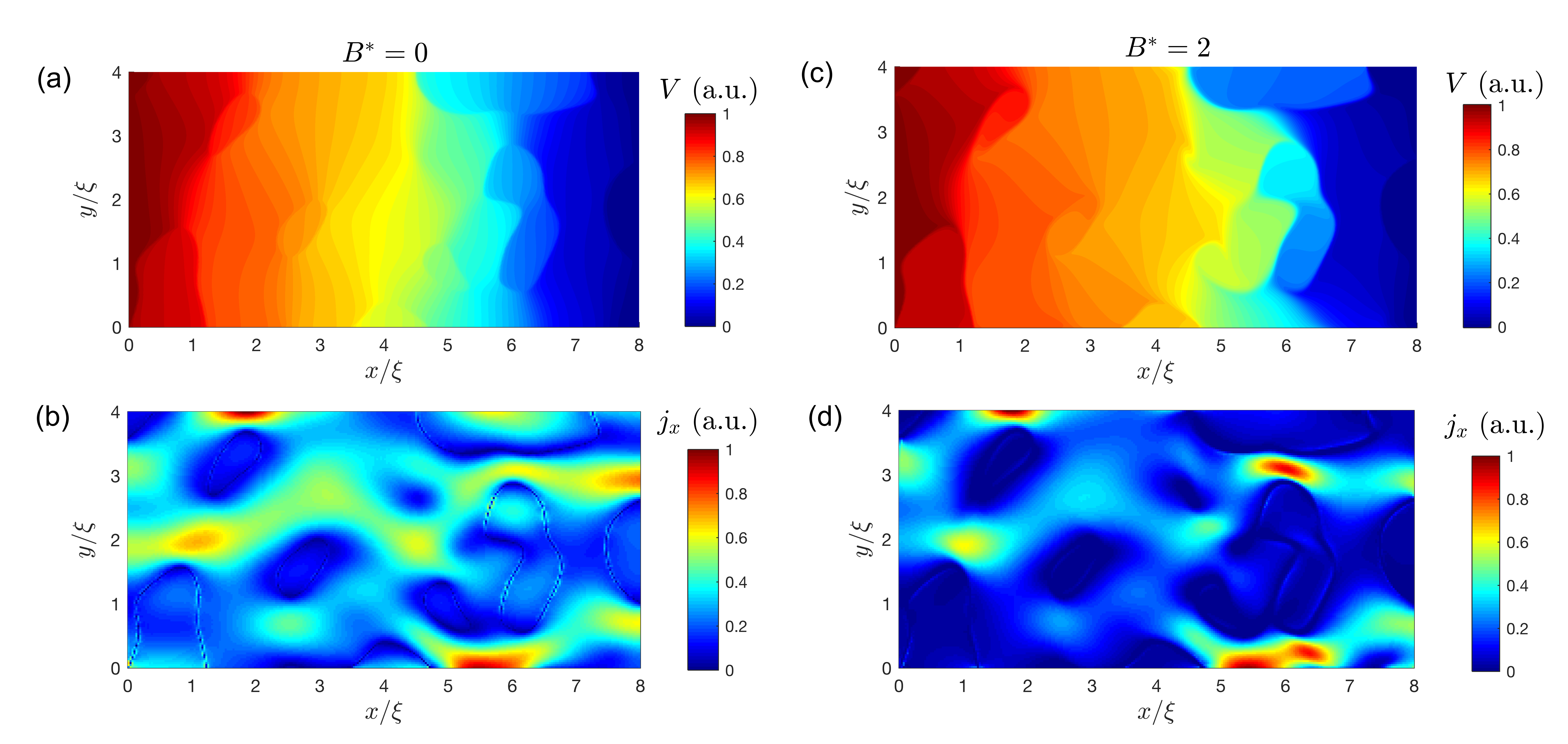
Figure 13 shows a typical numerical solution for the potential and the current in the direction at . Figures 13(a)-(b) show the potential and current at zero field, , while Figs. 13(c)-(d) show the same system at large field . One can see from these images the strong effect of “pinch points” in the random potential, where the current is concentrated at narrow constrictions between puddles. This focusing of the current becomes more exaggerated at large magnetic field, and correspondingly the electrochemical potential drops abruptly at pinch points and becomes relatively constant far from the boundaries between n- and p-type regions.
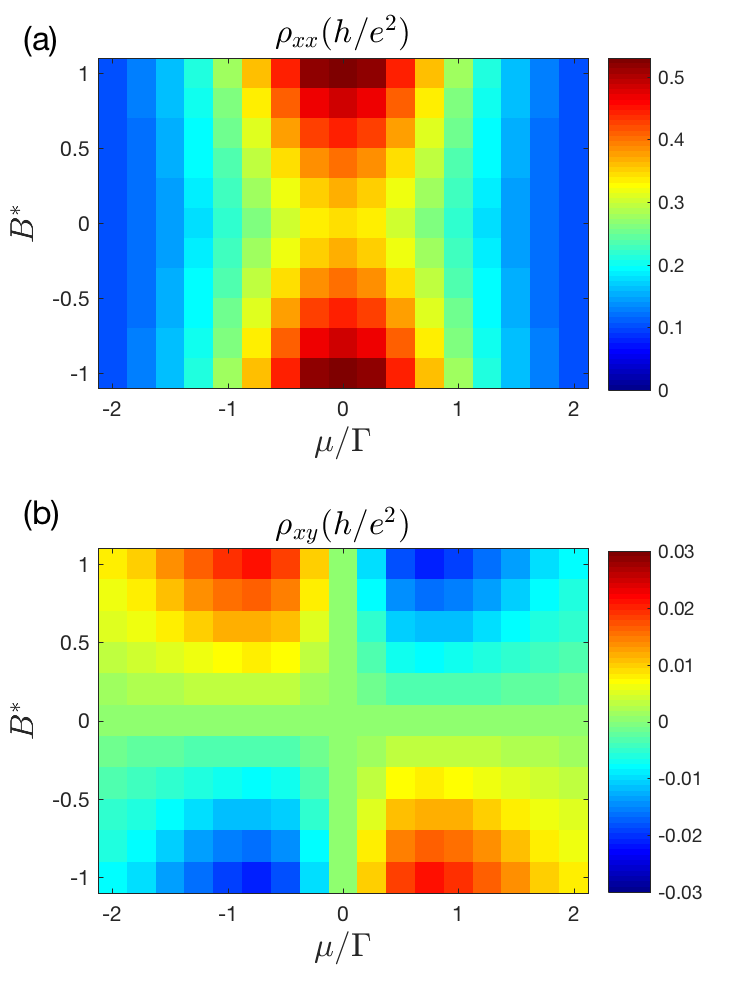
For a given realization of the random potential, the longitudinal resistivity can be defined from the simulation as , where is the area-averaged current density in the direction and is the voltage drop across the system. One can estimate the dependence of on magnetic field by averaging the simulated resistivity over many realizations of the random potential for a given value of . Our numerical results, including those shown in Fig. 8 of the main text, are averaged over 100 such realizations. One can also define the Hall resistivity by numerically extracting the transverse voltage across the Hall bar at the midpoint, , for a given realization. The Hall resistivity is defined by .
In Fig. 14 we show the values of and as produced by our simulation for a range of magnetic fields and . As in the experimental data (see Fig. 9), is much smaller than throughout the range of interest.
In order to fit the experimental data at to the numerical simulation, we calculate numerically the resistivity as a function of , using discrete points , for , and . Linear interpolation allows us to estimate the value of for generic values of between and and between and . The resulting curves can be translated into real units by inserting the corresponding values of and , which allows us to fit the data shown in Fig. 7(b) of the main text. The result of this fitting is shown in Fig. 8(b) of the main text, and corresponds to , and nm-1. This value of implies a typical electron/hole density cm-2, which is consistent in order of magnitude with both our theoretical estimates and our measurements of the Hall constant.
We extracted the dependence of the linear magnetoresistance slope on the chemical potential by numerically evaluating the curve for different values of , and then fitting each curve to a line over the range .
References
- Hsieh et al. (2009) David Hsieh, Y Xia, Dong Qian, L Wray, J H Dil, F Meier, J Osterwalder, L Patthey, J G Checkelsky, N P Ong, et al., “A tunable topological insulator in the spin helical dirac transport regime,” Nature 460, 1101–1105 (2009).
- Hasan and Kane (2010) M. Z. Hasan and C. L. Kane, “Colloquium,” Rev. Mod. Phys. 82, 3045–3067 (2010).
- Qi et al. (2009) Xiao Liang Qi, Rundong Li, Jiadong Zang, and Shou Cheng Zhang, “Inducing a magnetic monopole with topological surface states,” Science 323, 1184–1187 (2009).
- Essin et al. (2009) Andrew M. Essin, Joel E. Moore, and David Vanderbilt, “Magnetoelectric polarizability and axion electrodynamics in crystalline insulators,” Phys. Rev. Lett. 102, 146805 (2009).
- König et al. (2007) Markus König, Steffen Wiedmann, Christoph Brüne, Andreas Roth, Hartmut Buhmann, Laurens W Molenkamp, Xiao Liang Qi, and Shou Cheng Zhang, “Quantum spin hall insulator state in hgte quantum wells,” Science 318, 766–770 (2007).
- Roth et al. (2009) Andreas Roth, Christoph Brüne, Hartmut Buhmann, Laurens W Molenkamp, Joseph Maciejko, Xiao Liang Qi, and Shou Cheng Zhang, “Nonlocal transport in the quantum spin hall state,” Science 325, 294–297 (2009).
- Liu et al. (2010) Chao Xing Liu, HaiJun Zhang, Binghai Yan, Xiao Liang Qi, Thomas Frauenheim, Xi Dai, Zhong Fang, and Shou Cheng Zhang, “Oscillatory crossover from two-dimensional to three-dimensional topological insulators,” Phys. Rev. B 81, 041307 (2010).
- Nandi et al. (2018) D. Nandi, Inti Sodemann, K. Shain, G. H. Lee, K.-F. Huang, Cui-Zu Chang, Yunbo Ou, S. P. Lee, J. Ward, J. S. Moodera, P. Kim, and A. Yacoby, “Logarithmic singularities and quantum oscillations in magnetically doped topological insulators,” Phys. Rev. B 97, 085151 (2018).
- Yazyev et al. (2010) Oleg V. Yazyev, Joel E. Moore, and Steven G. Louie, “Spin polarization and transport of surface states in the topological insulators and from first principles,” Phys. Rev. Lett. 105, 266806 (2010).
- Jiang et al. (2012) Yeping Jiang, Yilin Wang, Mu Chen, Zhi Li, Canli Song, Ke He, Lili Wang, Xi Chen, Xucun Ma, and Qi-Kun Xue, “Landau quantization and the thickness limit of topological insulator thin films of ,” Phys. Rev. Lett. 108, 016401 (2012).
- Kim et al. (2011) Yong Seung Kim, Matthew Brahlek, Namrata Bansal, Eliav Edrey, Gary A Kapilevich, Keiko Iida, Makoto Tanimura, Yoichi Horibe, Sang Wook Cheong, and Seongshik Oh, “Thickness-dependent bulk properties and weak antilocalization effect in topological insulator bi 2 se 3,” Physical Review B 84, 073109 (2011).
- Zhang et al. (2010) Yi Zhang, Ke He, Cui Zu Chang, Can Li Song, Li Li Wang, Xi Chen, Jin Feng Jia, Zhong Fang, Xi Dai, Wen Yu Shan, et al., “Crossover of the three-dimensional topological insulator bi2se3 to the two-dimensional limit,” Nature Physics 6, 584–588 (2010).
- Skinner et al. (2013) B. Skinner, T. Chen, and B. I. Shklovskii, “Effects of bulk charged impurities on the bulk and surface transport in three-dimensional topological insulators,” Journal of Experimental and Theoretical Physics 117, 579–592 (2013).
- Stampfer et al. (2009) C. Stampfer, J. Güttinger, S. Hellmüller, F. Molitor, K. Ensslin, and T. Ihn, “Energy gaps in etched graphene nanoribbons,” Phys. Rev. Lett. 102, 056403 (2009).
- Lee et al. (2015a) Gil-Ho Lee, Dongchan Jeong, Kee-Su Park, Yigal Meir, Min-Chul Cha, and Hu-Jong Lee, “Continuous and reversible tuning of the disorder-driven superconductor–insulator transition in bilayer graphene,” Scientific reports 5, 13466 (2015a).
- Skinner et al. (2014) Brian Skinner, B. I. Shklovskii, and M. B. Voloshin, “Bound state energy of a coulomb impurity in gapped bilayer graphene,” Phys. Rev. B 89, 041405 (2014).
- Note (1) The theoretical estimates of Ref. \rev@citealpnumskinner2013theory are slightly modified for our case, since the two opposite TI surfaces screen the disorder in tandem and therefore the density of states should be doubled relative to the case of a single surface.
- Steinberg et al. (2011) H. Steinberg, J.-B. Laloë, V. Fatemi, J. S. Moodera, and P. Jarillo-Herrero, “Electrically tunable surface-to-bulk coherent coupling in topological insulator thin films,” Phys. Rev. B 84, 233101 (2011).
- Liu et al. (2012) Minhao Liu, Jinsong Zhang, Cui-Zu Chang, Zuocheng Zhang, Xiao Feng, Kang Li, Ke He, Li-li Wang, Xi Chen, Xi Dai, Zhong Fang, Qi-Kun Xue, Xucun Ma, and Yayu Wang, “Crossover between weak antilocalization and weak localization in a magnetically doped topological insulator,” Phys. Rev. Lett. 108, 036805 (2012).
- Tian et al. (2014) Jifa Tian, Cuizu Chang, Helin Cao, Ke He, Xucun Ma, Qikun Xue, and Yong P. Chen, “Quantum and classical magnetoresistance in ambipolar topological insulator transistors with gate-tunable bulk and surface conduction,” Scientific Reports 4, 4859 EP – (2014).
- Zhang et al. (2013) Li Zhang, Merav Dolev, Qi I. Yang, Robert H. Hammond, Bo Zhou, Alexander Palevski, Yulin Chen, and Aharon Kapitulnik, “Weak localization effects as evidence for bulk quantization in bi2se3 thin films,” Phys. Rev. B 88, 121103 (2013).
- Hikami et al. (1980) Shinobu Hikami, Anatoly I Larkin, and Yosuke Nagaoka, “Spin-orbit interaction and magnetoresistance in the two dimensional random system,” Progress of Theoretical Physics 63, 707–710 (1980).
- Wang and Lei (2012) C. M. Wang and X. L. Lei, “Linear magnetoresistance on the topological surface,” Phys. Rev. B 86, 035442 (2012).
- Chen et al. (2011) J. Chen, X. Y. He, K. H. Wu, Z. Q. Ji, L. Lu, J. R. Shi, J. H. Smet, and Y. Q. Li, “Tunable surface conductivity in bi2se3 revealed in diffusive electron transport,” Phys. Rev. B 83, 241304 (2011).
- Ilan et al. (2006) R. Ilan, N. R. Cooper, and Ady Stern, “Longitudinal resistance of a quantum hall system with a density gradient,” Phys. Rev. B 73, 235333 (2006).
- Parish and Littlewood (2005) Meera M. Parish and Peter B. Littlewood, “Classical magnetotransport of inhomogeneous conductors,” Phys. Rev. B 72, 094417 (2005).
- Kozlova et al. (2012) N. V. Kozlova, N. Mori, O. Makarovsky, L. Eaves, Q. D. Zhuang, A. Krier, and A. Patanè, “Linear magnetoresistance due to multiple-electron scattering by low-mobility islands in an inhomogeneous conductor,” Nature Communications 3, 1097 EP – (2012).
- Knap et al. (2014) Michael Knap, Jay D. Sau, Bertrand I. Halperin, and Eugene Demler, “Transport in two-dimensional disordered semimetals,” Phys. Rev. Lett. 113, 186801 (2014).
- Ping et al. (2014) Jinglei Ping, Indra Yudhistira, Navneeth Ramakrishnan, Sungjae Cho, Shaffique Adam, and Michael S. Fuhrer, “Disorder-induced magnetoresistance in a two-dimensional electron system,” Phys. Rev. Lett. 113, 047206 (2014).
- Ramakrishnan et al. (2017) Navneeth Ramakrishnan, Ying Tong Lai, Silvia Lara, Meera M. Parish, and Shaffique Adam, “Equivalence of effective medium and random resistor network models for disorder-induced unsaturating linear magnetoresistance,” Phys. Rev. B 96, 224203 (2017).
- Ruzin (1993) I. M. Ruzin, “Hall transport in nonuniform two-dimensional conductors,” Phys. Rev. B 47, 15727–15734 (1993).
- Hans and Friedrich (1958) Joachim Hans and Kuhrt Friedrich, “zna,” (1958) Chap. Der Geometrieeinfluß auf den transversalen magnetischen Widerstandseffekt bei rechteckförmigen Halbleiterplatten, p. 462, 6.
- Jensen and Smith (1972) H Hojgaard Jensen and H Smith, “Geometrical effects in measurements of magnetoresistance,” Journal of Physics C: Solid State Physics 5, 2867 (1972).
- Abanin and Levitov (2008) Dmitry A. Abanin and Leonid S. Levitov, “Conformal invariance and shape-dependent conductance of graphene samples,” Phys. Rev. B 78, 035416 (2008).
- Lee et al. (2015b) Joon Sue Lee, Anthony Richardella, Danielle Reifsnyder Hickey, K. Andre Mkhoyan, and Nitin Samarth, “Mapping the chemical potential dependence of current-induced spin polarization in a topological insulator,” Phys. Rev. B 92, 155312 (2015b).
- Fu and Kane (2008) Liang Fu and C. L. Kane, “Superconducting proximity effect and majorana fermions at the surface of a topological insulator,” Phys. Rev. Lett. 100, 096407 (2008).
- Tanaka et al. (2009) Yukio Tanaka, Takehito Yokoyama, and Naoto Nagaosa, “Manipulation of the majorana fermion, andreev reflection, and josephson current on topological insulators,” Phys. Rev. Lett. 103, 107002 (2009).
- Potter and Fu (2013) Andrew C. Potter and Liang Fu, “Anomalous supercurrent from majorana states in topological insulator josephson junctions,” Phys. Rev. B 88, 121109 (2013).
- Moore (2010) Joel E Moore, “The birth of topological insulators,” Nature 464, 194 (2010).
- Williams et al. (2012) J. R. Williams, A. J. Bestwick, P. Gallagher, Seung Sae Hong, Y. Cui, Andrew S. Bleich, J. G. Analytis, I. R. Fisher, and D. Goldhaber Gordon, “Unconventional josephson effect in hybrid superconductor-topological insulator devices,” Phys. Rev. Lett. 109, 056803 (2012).
- (41) Leonid P Rokhinson, Xinyu Liu, and Jacek K Furdyna, “The fractional ac josephson effect in a semiconductor-superconductor nanowire as a signature of majorana particles,” Nature Physics 8, 795.
- Kurter et al. (2015) C Kurter, A D Finck, Y S Hor, and D J Van Harlingen, “Evidence for an anomalous current-phase relation in topological insulator josephson junctions,” Nature communications 6, 7130–7130 (2015).
- Hart et al. (2014) Sean Hart, Hechen Ren, Timo Wagner, Philipp Leubner, Mathias Mühlbauer, Christoph Brüne, Hartmut Buhmann, Laurens W Molenkamp, and Amir Yacoby, “Induced superconductivity in the quantum spin hall edge,” Nature Physics 10, 638–643 (2014).
- Lee et al. (2014) Jae Hyeong Lee, Gil Ho Lee, Joonbum Park, Janghee Lee, Seung Geol Nam, Yun Sok Shin, Jun Sung Kim, and Hu Jong Lee, “Local and nonlocal fraunhofer-like pattern from an edge-stepped topological surface josephson current distribution,” Nano letters 14, 5029–5034 (2014).