Unveiling hidden charge density waves in single-layer NbSe2 by impurities
Abstract
We employ ab-initio calculations to investigate the charge density waves in single-layer NbSe2, and we explore how they are affected by transition metal atoms. Our calculations reproduce the observed orthorhombic phase in single-layer NbSe2 in the clean limit, establishing the energy order between three different distorted structures, two consisting of triangular Nb-Nb clusters and a third, energetically unfavoured, consisting of hexagonal Nb-Nb clusters. Such energy order, in agreement with known experimental work, is reversed by the adsorption of Co and Mn, which favour the formation of hexagonal Nb-Nb clusters; this CDW structure is indeed allowed from symmetry point of view but hidden in pure single layers because it is at a higher energy. The other adsorbates, K and Ga, still favour one of the triangular Nb-Nb cluster, while suppressing the other. We report how the energy difference between such distorted structure varies with these adsorbates. Furthermore, transition metals induce magnetism and favour the reduction of the symmetry of the charge density distribution.
I Introduction
Over the past decade, synthesis and exploration of atomically thin two-dimensional (2D) materials have almost revolutionised our common understandings of condensed matter systems and opened a new era in nanosciences Novoselov et al. (2005); Xu et al. (2013); Choi et al. (2017). In particular, 2D materials usually show drastically different electronic properties compared to their corresponding bulk structures composed of van der Waals (vdW) coupled atomic layers Butler et al. (2013); Geim and Grigorieva (2013); Novoselov et al. (2016). Transition metal dichalcogenides (TMDCs) are among vdW layered materials which show a wide range of interesting phenomena and applications due to the tunability of their electronic structures Splendiani et al. (2010); Mak et al. (2010); Kuc et al. (2011); Wang et al. (2012). Moreover, they can host exotic phases, such as superconductivity (SC), charge density waves (CDW), and even topologically non-trivial states Chhowalla et al. (2013); Frindt (1972); Wilson et al. (2001); Gong et al. (2017); Qi et al. (2016). Strongly correlated phases in bulk TMDCs have been well studied for decades, and recent observations of CDWs and Ising SC Lu et al. (2015) in few-layer films have revived interest in these materials Xi et al. (2015, 2016a); Ugeda et al. (2016); Xi et al. (2016b); Zhu et al. (2016).
Among TMDCs, NbSe2 has been considered as a prototype material for investigation of CDW orders and SC Bevolo and Shanks (1974); Corcoran et al. (1994). Bulk 2H-NbSe2 hosts a CDW phase with a periodicity below 33K which can coexist with an s-wave superconducting phase below 7K Wilson et al. (1974); Moncton et al. (1975); Revolinsky et al. (1965); Rahn et al. (2012); Castro Neto (2001), and it is known for its high magnetic anisotropy Galvis et al. (2018). By reducing its thickness down to single layers, the SC weakens but still survives, whereas the CDW transition temperature increases Frindt (1972); Xi et al. (2015); Ugeda et al. (2016). The SC-CDW coexistence in NbSe2 is due to a momentum dependent gap opening Rahn et al. (2012); Zheng et al. (2018) accompanied by an electronic reconstruction over a wide energy range Arguello et al. (2014), leaving enough electronic states available for the superconducting transition. Such SC-CDW coexistence is maintained with charge doping, and their order parameters vary in the same fashion Xi et al. (2016b). The origin of the CDWs has been intensively debated for some TMDCs, including NbSe2, mostly because of controversies over the role of Fermi-surface nesting Rice and Scott (1975); Liu et al. (1998); Straub et al. (1999); Inosov et al. (2008); Rossnagel et al. (2001); Rossnagel and Smith (2007); Johannes et al. (2006); Johannes and Mazin (2008). Nevertheless, in recent years theoretical and experimental evidences has been accumulated in support of momentum-dependent electron-phonon coupling as a key mechanism in the formation of CDWs Calandra et al. (2009); Valla et al. (2004); Zhu et al. (2015); Arguello et al. (2015). Turning to 2D single-layers, the lack of inversion symmetry, the disappearance of the coterminous of vdW interactions and the interplay with many-body strong-correlation effects may lead to the aforementioned drastic changes Kotov et al. (2012); Guinea et al. (2014); Mak et al. (2012).
On the other hand, the structure of CDWs in bulk and single-layer NbSe2 is controversial Skripov and Stepanov (1985); Malliakas and Kanatzidis (2013); Ángel Silva-Guillén et al. (2016). While a recent detailed experimental work reported evidence of a commensurate modulation of the crystal structure, the case of the single-layer still needs to be clarified Calandra et al. (2009); Malliakas and Kanatzidis (2013). In addition, impurities or gate doping can play a major role on the CDW behaviour. For example, long-range CDW phase coherence can be suppressed in NbSe2 by a moderate percentage of Co or Mn intercalated at the surface Chatterjee et al. (2015), Na intercalated in a bi-layer Lian et al. (2017) and electron doping Xi et al. (2016b), whereas it can be increased by hole doping Xi et al. (2016b). Besides, Bi adsorption can also lead to a transition to a stripe phase Fang et al. (2018), previously observed in accidentally doped samples Soumyanarayanana et al. (2013).
In this work, performing an exhaustive first principle calculations, we reveal possible structures of CDWs, particularly at the presence of certain types of impurities. Among three different modulated structures, those two with triangular Nb-Nb clusters are found to be energetically favoured in clean NbSe2 2D sheet. These results are consistent with experimental evidence Skripov and Stepanov (1985); Malliakas and Kanatzidis (2013). As a key finding we demonstrate that CDWs with hexagonal modulation can be established by adsorption of certain atoms such as Co and Mn. This type of CDW phase is in fact hidden in pristine NbSe2 because it has a higher energy compared to triangularly-modulated CDWs. In addition, it is uncovered that the presence of the transition metal impurities induces magnetism and promotes modulated phases with reduced symmetry of the charge density distribution compared to pure CDW structures. Other types of metallic ad-atoms, namely K and Ga, allow the same ground state as pristine single-layer NbSe2, but Ga also supports the hexagonally modulated structure. The current manuscript aims at steering future research towards a new interpretation of the experimental evidence on the effect of impurities Fang et al. (2018); Chatterjee et al. (2015); Soumyanarayanana et al. (2013), and represents an important contribution in the field of the interplay between CDWs and SC, as a recent work strongly points out Cho et al. (2018).
This paper is organised as follows. In Sec. II, we will briefly introduce the computational method based on density functional theory which is used for investigation of CDW phases. Thereafter, we go through the results of ab-initio calculations for CDWs in pristine NbSe2, Sec. III, where the relaxed CDW structures and the profiles of charge densities are presented both in real space and in Fourier transformed form. The core of our work is found in Sec. IV, which shows the CDWs in the presence of various impurities. In particular, we show how the energy hierarchy of the CDWs can be different from the pristine system and a hidden order arise as a new ground state by adding Co or Mn ad-atoms. Finally, after a discussion over the results, the conclusions are presented in Sec. V.
II Computational details
Our results are obtained by means of density-functional theory (DFT). We employ the projected augmented wave (PAW) method with Perdew-Burke-Ernzerhof (PBE) pseudopotentials, as implemented in the Vienna ab initio Simulation Package (VASP) Blöchl (1994); Kresse and Joubert (1999). Accordingly, the exchange-correlation functional is treated in the generalised gradient approximation in the PBE parametrisation Perdew et al. (1996, 1997). The basis set consists of plane waves, with the explicit treatment of 13, 6, 9, 15, 9 and 13 valence electrons for Nb, Se, Co, Mn, K and Ga states, respectively. As previously suggested Wehling et al. (2011), standard local and semi-local exchange-correlation functionals may not offer a proper description of the partially filled and shells of TM adatoms on 2D materials. Therefore, calculations involving Co and Mn are performed in the DFT+U approach, using the rotationally invariant formulation of Lichtenstein et al. Liechtenstein et al. (1995). As in ref. Wehling et al., 2011, we use a generalised value of eV and eV for the orbitals of both Co and Mn. Small variations of these parameters (within a reasonable range) are unlikely to change the physical picture outlined in the present paper. For sake of completeness we analyse this issue for Co adatoms, in the Appendix. For all calculations, the cutoff energy of the plane waves is 400 eV, while the energy tolerance on the electronic loops for the relaxation and for the electronic properties are set to 10-6 eV and 10-7 eV, respectively; a conjugate gradient algorithm is employed for structural relaxation. Structures are considered relaxed when the forces on each atom are smaller than 2 meV/Å. The simulations are run in , and replicas of the NbSe2 single-layer unit cell. After convergence tests on the k-meshes for the and replicas were performed, , and grids of k-points were used to sample their Brillouin Zones for the total energy calculations; and k-meshes were used for the partial charge density calculations in the and replicas, respectively; a k-mesh was used for the DOS calculations in the replica. In modelling metal adsorption on NbSe2, the concentration of one ad-atom in a replica of the unit cell was adopted, corresponding to 0.0278 impurities/f.u., which allows for a description of a CDW while minimising the interaction between impurities and their images. The adsorbates taken into account in the present study are Co, Mn, K and Ga.
III CDW phases in pristine single layers
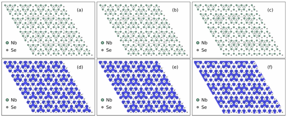
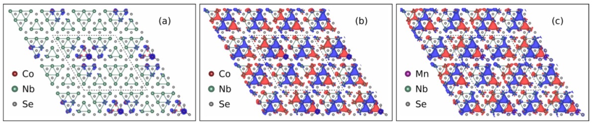
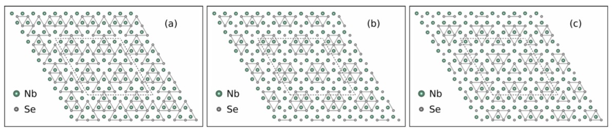
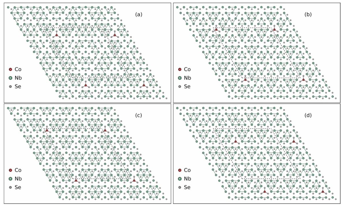
We begin with the study of the single-layer NbSe2 in a supercell, which is the minimal size cell for a CDW in NbSe2. Pristine single-layer NbSe2 is known to be metallic, non magnetic and hosts CDWs below 145 K Wilson and Yoffe (1969); Moncton et al. (1975); Wilson et al. (2001). Our models include three structures obtained according to existing work Skripov and Stepanov (1985); Malliakas and Kanatzidis (2013); Xi et al. (2015), which are shown in Fig. 1; the Nb atoms cluster in triangular patterns - see Figs. 1(a and b) - and hexagonal ones - see Fig. 1 (c); the two triangular patterns differ by the position of the Se atoms with respect to the triangle composed by the Nb-Nb bonds; accordingly, the CDW structures are named T-U, T-C and HX, respectively (T-U and T-C stand for triangle-uncentred and triangle-centred, whereas HX stands for hexagonal). The two structures T-U and T-C are related to each other by a mirror reflection of the Nb sublattice. It is also known that the Se-Se bond patterns (analogous to Nb-Nb bond patterns) accompany those of Nb-Nb Ángel Silva-Guillén et al. (2016). The T-U and T-C CDWs differ for the Se-Se pattern, see the Appendix for details. Their total energies were compared in and replicas of the NbSe2 unit cell, and suggest that the formation of all of them is favoured. The T-U is the lowest energy CDW structure; calculations in the supercell yield differences of 3.9 meV, 0.5 meV and 1.3 meV/f.u. with respect to the undistorted structure, T-C and HX, respectively. In the supercell, slight changes are observed in the energy differences between the CDW structures: the T-U is favoured by 0.4 meV and 1.1 meV over the T-C and HX, respectively; these differences are maintained for a supercell. The three CDW structures were recently investigated elsewhere on supercells Lian et al. (2018). Here, we demonstrate our agreement with ref. Lian et al., 2018, and we make use of the results for the pristine to compare the metal-adsorbed NbSe2.
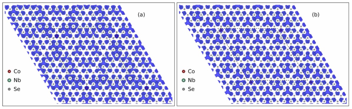
The effect of the CDW distortions on the density of states (DOS) is analysed in the Appendix. For what concerns the electronic reconstruction following the CDW formation, our calculations are in agreement with the literature Shen et al. (2007); Calandra et al. (2009). The charge distributions are computed integrating the charge density over the occupied Nb band (the band crossing Fermi level, see the Appendix) and they are shown in Fig. 1, second row. The integration over the whole occupied band simulates a topography retaining the symmetry of the Nb band only. The charge density clusters in patches, with different shape and patterns for each CDW; the lowest energy CDWs, T-U and T-C, have three-fold symmetric patterns and the HX CDW has six-fold symmetric ones. The patches of T-U are on the vertices of a hexagon (with no element on the centre), whereas those of T-C and HX are placed on the vertices and centre of a larger hexagon.
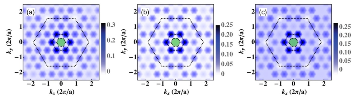
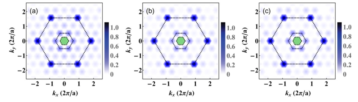
The Fourier Transform (FT) of the charge density distribution allows to recognise more clearly the symmetry of the modulation patterns and trace their length scale. Due to the three-dimensional periodic boundary conditions, the three-dimensional data is originally computed as a function of the Miller indices; the subset with is analysed to track modulations of the CDW charge distributions only along the plane. Thus, the FT is mapped as a function of and ( and in the relative plots). The computed FT plots of the charge density distributions of the three CDW structures in pristine NbSe2 are reported in Fig. 11, in Appendix A.
More significant information can be obtained by considering the difference between those plots and the FT plot of the charge density distribution of the non-modulated structure, shown in Fig. 2. In these (and following) plots, the vertices of the large hexagon, at , mark the position of the characteristic Bragg peaks, which are evident in Fig. 11. The vertices of the medium size hexagon, at , mark instead the position of the shorter peaks associated to the CDW. Both hexagons are emphasised with a dashed line, as a guide for the eye. The small green shaded hexagon, whose vertices are at , map points beyond the supercell borders, and thus are not meaningful. Due to the size of the supercell, the width of the spots denoting Bragg peaks or CDW peaks is large because different but close modulation frequencies cannot be resolved, even with a relatively dense k-mesh. Fig. 2 show the relative differences between the three CDWs and the non-modulated structure. The CDW main peaks are not sensibly different from plot to plot, neither are satellite peaks at and at . However, a sizeable satellite peak appears at in the T-U CDW, but not (as large) in the T-C nor in the HX CDWs. Such configuration of peaks mirrors the configuration of the electronic patches in Fig. 1, which in the T-U (T-C and HX) are placed at the vertices of a small (large) hexagon, without (with) a central element. In fact, two different vectors map equivalent patterns in T-U. Naming the lattice vectors of the unit cell and , the mapping vectors are (and equivalently ) and ; the latter does not map equivalent patches in T-C nor in HX.
| E | ||||
|---|---|---|---|---|
| hollow | 16 | 1.9 | 2.2 | |
| Co | top Nb | 0 | 1.9 | 2.0 |
| top Se | 3551 | 2.0 | 3.4 | |
| hollow | 91 | 4.4 | 5.8 | |
| Mn | top Nb | 0 | 4.4 | 4.3 |
| top Se | 1291 | 4.9 | 4.1 | |
| hollow | 4 | 0.0 | 5.9 | |
| K | top Nb | 0 | 0.0 | 0.0 |
| top Se | 241 | 0.0 | 1.2 | |
| hollow | 183 | 0.0 | 5.9 | |
| Ga | top Nb | 0 | 0.0 | 0.0 |
| top Se | 605 | 0.0 | 0.2 |
| pristine | Co | Mn | K | Ga | |||||
|---|---|---|---|---|---|---|---|---|---|
| T-U | (0.0) | T-U | (0.7) | T-U | (1.5) | T-Uh | (0.0) | T-U | (0.0) |
| T-U | (2.6) | T-UN | (0.2) | ||||||
| T-C | (0.4) | HX-A | (0.0) | HX-A | (0.0) | T-CN | (1.5) | HX-A | (0.1) |
| T-Ch | (1.3) | ||||||||
| HX | (1.1) | HX-S | (0.0) | HX-S | (0.0) | HX-S | (0.7) | HX-S | (0.0) |
| HX-A | (0.0) | HX-A | (0.0) | ||||||
| T-U | 1.9 | 2.0 | 3.440 | |
|---|---|---|---|---|
| Co | HX-A | 1.9 | 2.0 | 3.504 |
| HX-S | 1.9 | 1.9 | 3.504 | |
| T-U | 4.4 | 4.4 | 2.472 | |
| Mn | HX-A | 4.4 | 4.4 | 2.559 |
| HX-S | 4.4 | 4.3 | 2.561 | |
| T-Uh | 0.0 | 0.0 | 3.045 | |
| K | T-UN | 0.0 | 0.0 | 3.038 |
| HX-S | 0.0 | 0.1 | 3.060 | |
| T-U | 0.0 | 0.0 | 2.907 | |
| Ga | HX-A | 0.0 | 0.0 | 2.946 |
| HX-S | 0.0 | 0.0 | 2.944 |
IV CDW phases in the presence of impurities
Adsorption of the adsorbates Co, Mn, K and Ga on a fully symmetric structure induces structural distortions breaking the symmetry of the NbSe2 layer according to the site: the adsorption on the Nb site, hollow site and Se site induces CDWs of HX type (i.e. having similar Nb-Nb distance patterns to the pristine HX), T-U type and T-C type, respectively. By total energy calculations, the likelihood of the adsorption sites is analysed. The energies for different adsorption sites of the investigated ad-atoms are reported in Table 1. These results are consistent with those reported in a recent work on MoS2 Wei et al. (2017). The preferred adsorption site is on top of a Nb atom for Co, K, Ga and Mn. The competition between hollow site and Nb site is strong in the case of K (4 meV difference). The Se site remains the most unfavoured for single atoms. However, it competes with Nb for larger molecules. In order to highlight this trend, we computed the energy difference for Co-(OH)2, which can be considered as a prototype of a small molecule and a possible impurity. In the case of a single Co, the Nb site is preferred to the hollow site and Se site by 16 meV and 3551 meV, respectively; in the case of Co-(OH)2, the corresponding energy difference are 670 meV and 166 meV, suggesting a hindrance to the Co-Se bonds and Co-Nb bonds or a decrease of the Co charge state and in turn of its coordination. In summary, single Co is preferably adsorbed on the Nb site, with the hollow site relatively close in energy; large molecules favour adsorption on the Se site and unfavour adsorption at the hollow site, a trend in line with combined theoretical and experimental results Kezilebieke et al. (2018). After establishing the preferred adsorption sites on the NbSe2 non modulated structure for each adsorbate by total energy calculations, the adsorption on the different CDW structures is modelled (it involves different inequivalent adsorption sites due to the lower symmetry).
| Co | Mn | |||
|---|---|---|---|---|
| 0.93 | 0.07 | 0.93 | 0.03 | |
| 0.90 | 0.79 | 0.92 | 0.08 | |
| 0.95 | 0.92 | 0.93 | 0.09 | |
IV.1 Adsorption of Co
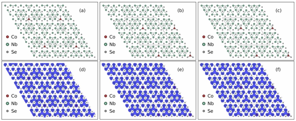
Upon adsorption of Co, the energy and state of CDWs are modified. In general, the solutions are a combination of the states found in the pristine system. Pure solutions of the T-U CDW are found and are referred to as such in the remainder. The HX CDW solutions are found in mixed states or pure states; those with lowest energy are grouped according to the symmetry of their structures and charge densities, and named HX-S and HX-A, for symmetric and asymmetric ones, respectively. The T-C CDW solutions are found only mixed (with the HX-A CDW). The HX-S, HX-A and T-U CDWs structures are shown in Figs. 3 (a), (b) and (c), respectively. The HX-S features the characteristic hexagonal patches of the pristine HX CDW together with a tri-fold symmetric star of Nb-Nb bonds, compare Figs. 3 (a) and 1 (c). Their charge density distributions are not remarkably different from their pristine counterparts, compare Figs. 3 (d) and 1 (f). The flatness of the (multi-dimensional) potential energy surface allows adsorption on different sites of the underlying CDW structure to give different solutions. As Table 2 reports, the HX-A CDW results from the relaxation of the adsorption of Co on the vertex of the large triangle of a T-C CDW structure, compare Fig. 1 (b), and a mixing between the T-C and the HX CDWs occurs. The patches in the charge density distribution, Fig. 3 (e), recall those in both the pristine T-U and the pristine T-C, Figs. 1 (e) and (f), supporting the previous observation. Finally, the structure and charge density distribution of the T-U solution are virtually identical to those in the pristine T-U CDW, with minor differences around the adsorption site, compare Figs. 3 (f) and 1 (a).
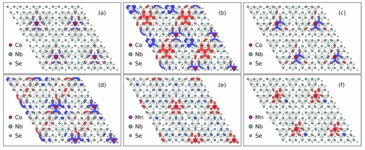
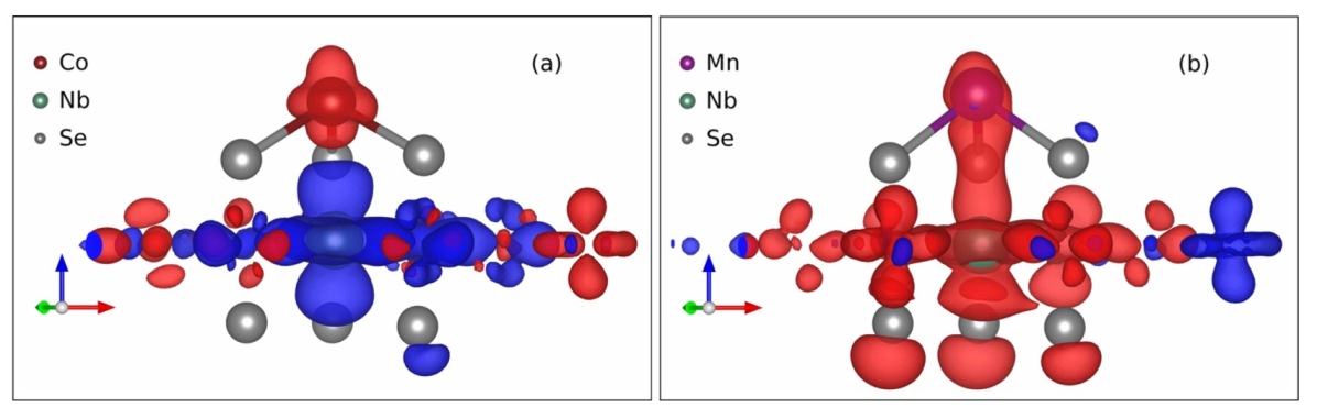
The magnetic density distributions exhibit antiferromagnetic coupling between Co and Nb in the occupied Nb band; moreover the magnetisation around Co in that energy range is opposite to the total magnetisation on Co, compare Fig. 4, first row, with Table 3. The magnetic moment on Co (value integrated over all the occupied states) is around 2.0 for every CDW, and the total magnetisation over the whole NbSe2 layer vanishes. The same observation is valid for Mn, see Table 3, and the discussion in the Appendix. The modulation of the magnetisation density in the HX-A CDW is larger than that in the HX-S (and that in T-U) CDW, compare Figs. 4 (a) and (b), first row, suggesting that larger mixing of different CDWs supports the formation of a spin density wave (SDW). Moreover, a different modulation of the magnetisation densities of CoNbSe2 T-U with Co at different adsorption CDW site is observed, compare Figs. 4 (c) and (d). These two structures are at the same energy, suggesting that a magnetic order transition is still incipient. The magnetisation data obtained by a site-by-site analysis point to a ferromagnetic coupling, in agreement with ref. Zhou et al., 2012, where an incipient magnetic transition is achieved by tensile strain.
The variation of the charge modulation can be analysed looking at the difference in the charge density distribution between CoNbSe2 CDWs and the pristine CDWs in the direct space, see Fig. 3. In these plots, blue (red) lobes denote injection (depletion) of charge with respect to the pristine CDW charge distribution. The adsorption of Co modifies the T-U CDW only in the neighbourhood of the adsorption site, see Fig. 5 (a), as expected from Fig. 3 (f); charge depletion (injection) occurs out-of-plane (in-plane) in correspondence to the Nb at the adsorption site and in a more complex pattern on the surrounding Nb atoms; in general, red lobes point towards the adsorbate. The charge difference between the HX-A and the T-U CDWs features a constant charge difference - due to the misalignment between the two charge densities (in NbSe2 and CoNbSe2) - and an enhancement of in-plane modulations identified by the isolated blue lobes in Fig. 5 (b); these may be more relevant in comparison to the out-of-plane modulations represented by the out-of-plane red lobes on isolated Nb atoms in Fig. 5 (c), which refer to Mn-adsorbed NbSe2.
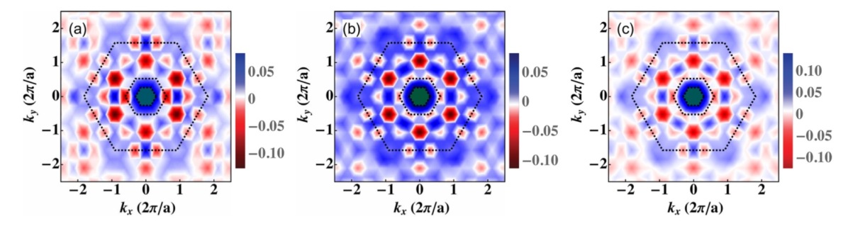
Eliminating charge displacements (due to the different adsorption sites) helps analysing the symmetry of the charge distribution. In analogy to what done for the pristine case (Fig. 2), we do not show the FT plots of the charge density distributions directly. Instead, we focus on the differences between these plots and the FT plot obtained for the T-U CDW in the pristine case. In order to identify variations in the CDW signal, the marks of Bragg peaks, CDW peaks and the region corresponding to points in the direct space beyond the supercell size are used in agreement with Figs. 2.
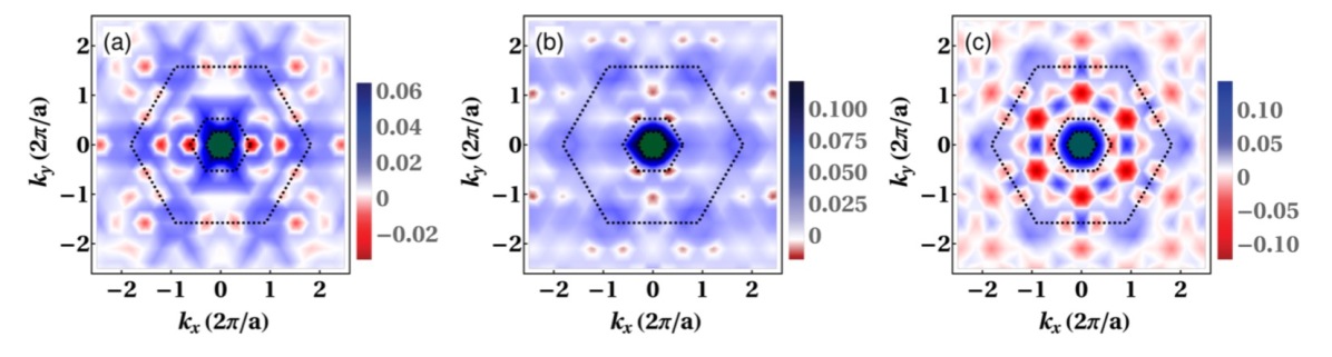
The FT plots relative to CoNbSe2 HX-A, CoNbSe2 HX-S and MnNbSe2 HX-A are shown in Figs. 6 (a)-(c); the FTs shown are computed difference with respect to the pristine T-U CDW. In these cases with adsorbates, a peak in the neighbourhood of appears, because of the background charge (uniformly) injected into the system. All plots in Fig. 6 point to a considerable suppression (enhancement) of the CDW intensity along at (at ); such suppression/enhancement is anisotropic for Co HX-A, being large along the line and small along the other two lines; the other cases are isotropic (Co HX-S) or virtually isotropic (Mn HX-A). Furthermore, large depletion of intensity at along as well as at along , illustrates again the difference between the pristine HX CDW (T-C as well) and the pristine T-U CDW observed above. Finally, intensity enhancement occurs also within the small hexagon marking the CDW peaks (but with no leading -vector), suggesting a competition between modulations with different wavelengths, as previously discussed Calandra et al. (2009); Lian et al. (2018). Indeed, strain-induced modifications of the vector were recently found Gao et al. (2018). In general, the asymmetric form of the CDW intensity (with respect to pristine T-U) suggests a connection with recently observed stripe phases Soumyanarayanana et al. (2013); Fang et al. (2018); Gao et al. (2018) of which it could be a precursor. The character of the asymmetry in the adsorbates systems is further treated in the Appendix, with reference to Fig. 14.
IV.2 Adsorption of Mn
In the case of Mn adsorption, magnetism plays a major role. A high magnetic moment, which correctly describes Mn, favours the Nb site more than in the case of Co adsorption (the energy difference between the Nb site and the hollow site is 5 times larger), compare their energy differences in Table 1. The ordering of the CDW structures, assessed by total energy calculations, follows the same pattern as in the case of Co adsorption, having a family of ground state HX CDWs, including a symmetric one and an asymmetric one, a solution of T-U at a higher energy and the absence of a T-C solution. The energy difference between the ground state HX CDW and the T-U solution is 1.5 meV/f.u., see Table 2, which compared to the case of Co, it suggests that Mn drives a slightly stronger transition to a HX CDW. The charge density distributions of the HX-S and HX-A show no essential difference, being also very similar to that of CoNbSe2 HX-S. Therefore, the relative figures are omitted, and the remaining discussion is limited to the magnetisation density distributions and the FT of the charge density distributions.
The magnetisation densities of the HX-S, HX-A the T-U are shown in Fig. 4, second row. The two HX CDWs are similar also in their magnetisation density distribution - compare with the case of Co adsorption, Fig. 4, second row. The structure of HX-A has a reflection symmetry through the top-left to bottom-right diagonal as represented in Fig. 4. The T-U CDW structure is modified slightly in the vicinity of the adsorption site. The magnetisation density in all of the CDWs is negative around Mn, unlike the case of Co, where a negative cloud surrounding Co is neighboured by a positive cloud around the closest Nb atoms, compare also Figs. 17 (a) and (b) in the Appendix, showing a detailed view on the vicinity of the adsorption sites.
Charge density differences in direct space are analysed in comparison with Co adsorption. The main difference between the two adsorbates is that with Mn adsorption the out-of-plane charge modulations are not suppressed. In fact, note that the in-plane red lobes in Fig. 5 (e) replace the out-of-plane red lobes in Fig. 5 (c), point in three directions, symmetrically. In fact, the similarity between Figs. 5 (d) and (f) confirms that the HX-S has the same features in the case of Co and Mn, with blue lobes pointing out-of-plane.
The analysis of the FT plots was mentioned previously with reference to Fig. 6. The main difference with the case of Co adsorption is that the HX-A and HX-S do not differ much, i.e. the intensity variation shows little contrast between the and the symmetries, compare the HX-A and HX-S CDWs in Figs. 6 (c) and 14 (c). The preference of the TM for the HX CDWs seems to be at variance with their tendency of reducing the symmetry from to . The lowest energy solutions for CoNbSe2 (and MnNbSe2) are mixed state of HX and T-C CDWs, compare Fig. 3 (b) with Fig. 1 (b). However the CoNbSe2 HX-A CDW solution has a consistent T-C component, whereas the MnNbSe2 HX-A CDW solution has a small T-C component, see the underlying structure in the magnetisation density plot, Fig. 4 (e).
The CDW solutions for TM adsorbates on NbSe2 are in fact mixed states; where the mixing between HX and T-C is high, the symmetry of the charge density distribution is reduced, whereas predominant HX CDW solutions keep a symmetry. In the case of Mn, the preference for HX solutions is higher than in the case of Co, and as a result the T-C component in the mixed solutions is smaller and in turn the symmetry is virtually maintained. Finally, the observation that the T-U / T-C have a reduced symmetry, raises the question on pristine T-U/C and the symmetry of its charge density distribution, which has a symmetry; perhaps the adsorbates induces some symmetry breaking which allows the T-U to undergo a transition.
Table 4 shows the occupancies of Co and Mn orbitals. The environment around the TM in the NbSe2 layer is trigonal prismatic, and therefore orbitals split into three groups due to the crystal field; these are classified according to their symmetry into , and . The orbital splitting is valid also for Co and Mn orbitals, but the intensity of the splitting is reduced because the environment is incomplete. Therefore, the spin splitting, which depends on the -character of the orbitals is larger than or comparable to the crystal field splitting, and orbitals are ordered by increasing energy as follows: in the majority spin channel, , and ; in the minority spin channel the order of and is inverted. Furthermore, the orbital projections onto cubic (real spherical) harmonics (, , , and , ordered by increasing value) are spin dependent. The orbitals of the eigenbasis can be written as , , and . (Freedom in the choice of the basis set allows one to set .) The -character of the orbitals is close to 1 (i.e. the values are larger than the values); conversely, the orbitals have a prevalent character ( values are larger); overall, this fact holds for the and orbitals.
In summary, TM adsorption favours HX CDW, weakening the CDW signals for the T-U and T-C CDWs, and the symmetry of the charge distribution is reduced from to , especially in the case of Co, where mixing between HX and T-C occur. The modulation of the magnetic density is dependent on the symmetry of the charge distribution: the higher the symmetry, the weaker the modulation. Also, due to a weaker crystal field splitting, the orbital order of the of Co and Mn in the two spin channels is different. Finally, a probe for Mn and Co is given in terms of -character of their electrons.
IV.3 Adsorption of K and Ga
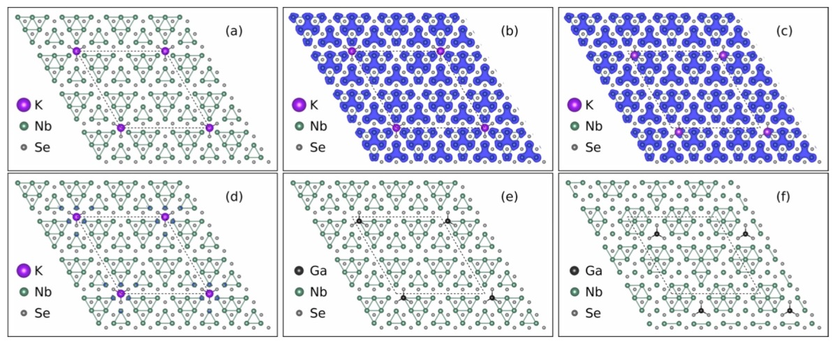
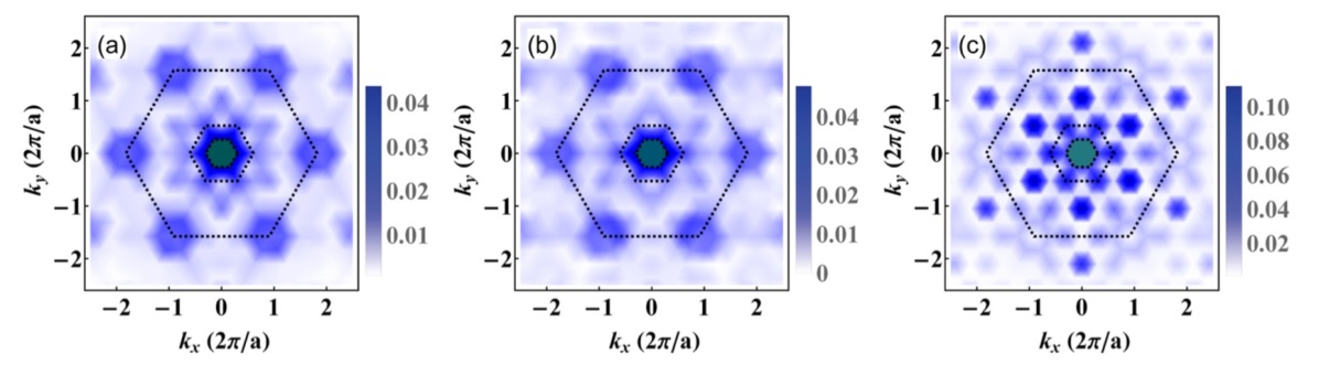
The adsorption of K is different from the other cases, since the energy difference between having an adatom at the hollow site or in top of a Nb site (see Table 1) is small, and therefore can be reversed by the presence of a CDW. This is, in fact, what happens. While on a non modulated NbSe2 structure, the hollow site stands 4 meV above the Nb adsorption site, on the CDW modulated structures the hollow site becomes more favourable, of about 0.2 meV/f.u. (their respective ground state are compared). The solutions obtained starting from the T-C converge to mixed states between T-C itself and HX and they are found at a high energy, while the T-U CDW is still favoured by 0.7 meV/f.u. over the HX CDW (the energy difference slightly changes with respect to the pristine case). The CDW structure and charge density distribution (in the T-U) on the hollow site (the ground state) and on the Nb site look very similar, see Fig. 7, and trace back to the pristine CDW ground state, compare Fig. 1. The CDW is slightly enhanced inside the hexagon delimiting the CDW peaks, but without a leading . The symmetry of the FT plot for K on the Nb (hollow) site is reduced from C6 to C2 at the points (), see Fig. 8; however, the intensity is one order of magnitude smaller than that of the Nb and Mn cases. Note also the difference with the T-C CDW, showing that the signal of K-adsorbed T-U on the hollow site is significantly enhanced with respect to pristine T-C at distinct vectors, see Fig. 8 (c).
The case of Ga is interesting in comparison with K because Ga has a fully occupied shell and a single electron in the shell. In this case, the adsorption on the Nb site is favoured by 183 meV over the adsorption at the hollow site. The T-U CDW is in strong competition or coexists with the HX CDW, and the T-C converges to a mixed solution between T-C and HX, analogously to the case of K. The ground state structures are shown in Fig. 7. The charge density distributions and their FTs are not particularly different from the case with K adsorption. Both K and Ga cases are related to gate doping, because they consist of an electron per 36 f.u. injected in the system. However, structural reconstructions due to the chemical adsorption must be considered for the enhancement or suppression of the CDW order. Compared to experimental observations with gate doping Xi et al. (2016b), where the case of K and Ga adsorption suppress the CDW order, the FT plots suggest that a considerable order remains (no depletion is seen at any ). Therefore, a doping with a hole carrying atom could enhance the CDW signal.
Overall, adsorption of atoms on single-layers NbSe2 suppresses the T-C CDW and promotes the HX CDWs in all cases; in particular, with Co and Mn the HX CDWs become the ground state for all the coverage considered in this study, whereas in the case of Ga the HX CDWs are at the same energy of the T-U CDW. Adsorption of K does not change the ground state (T-U) but does suppress the T-C CDW; the HX CDW solutions are the closest ones to the ground state (0.7 meV/f.u. above it), within thermal fluctuations, and therefore they are very likely to be seen by Scanning Tunnelling Microscopy in real samples. In fact, as several STM data are becoming available, a guide on the CDW hierarchy may be very useful to correctly identify and locate metallic impurities in TMDCs.
A detailed comparison between theory and experiment requires also an analysis of the role of the substrate, which may induce a variety of effects, as e.g. in-plane strain and charge transfer. Recently, single layers were grown on bi-layer graphene, and a CDW order slightly weaker compared to the bulk was reported Ugeda et al. (2016); however, the phase competition between different modulations was not investigated. Our study suggests, based on the few examples analysed, that one CDW phase (T-U) is suppressed with respect to other hidden ones (HX). As a concluding remark, we observe that the symmetry of the charge density distribution is reduced from to , hinting to a weakening of a -vector, which may be the precursor of a stripe phase recently observed by STM Fang et al. (2018); Soumyanarayanana et al. (2013).
V Conclusions
By means of ab-initio calculations based on total energy and direct space charge computation, we have investigated the existence and competition of CDWs in single-layer NbSe2 without and with impurities. The T-C CDW is suppressed in all cases, suggesting that its observation in STM images is unlikely in non-passivated samples, due to the high reactivity of NbSe2 and, in general, metallic TMDCs. Transition metal adsorbates invert the energy hierarchy between CDWs, favouring the HX CDWs over the T-U and the T-C. Adsorption of K keep the T-U CDW as the ground state, although the HX CDW is preferred to the T-C CDW; adsorption of Ga equally favours the T-U and the HX CDWs pointing to a coexistence. In general, adsorption of atoms, changing the local symmetry mixes the ‘pristine’ CDWs, in particular the HX and the T-C. The symmetry of the charge density distribution is reduced from to upon Co or Mn adsorption. Future research will be focused on understanding the role of the substrate in the stabilisation of the CDWs, in order to have a better correspondence between theory and experiment.
Acknowledgements
We are grateful to B. I. Min, V. Fiorentini, E. Tosatti and D. Payne for fruitful discussions. This research work was supported by the Ministry of Education, Gyeongsangbuk-do and Pohang City, through the National Research Foundation of Korea (Grant Nos.: 2015R1C1A1A01052411 and 2017R1D1A1B03033465). K. K. and A. A. acknowledge the Max Planck POSTECH / KOREA Research Initiative programs through the National Foundation of Korea (NRF) funded by the Ministry of Science, ICT and Future Planning (Grant No. 2016K1A4A4A01922028). The computational work was performed on resources provided by the Swedish National Infrastructure for Computing (SNIC) at the High Performance Computing Center North (HPC2N), at the PDC center for High Perfomance Computing and on the National Computational Infrastructure (NCI) of Australia. Further computational resources were provided by the IBS centre at POSTECH and the Korean Institute of Science and Technology Information (KISTI).
Appendix A Pristine
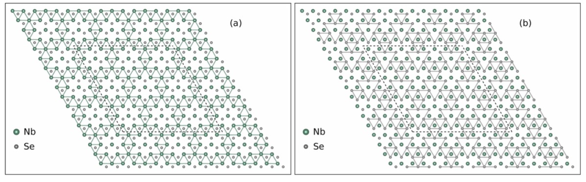
As reported in the literature, the (multi-dimensional) potential energy surface of the CDW phase features several (rather shallow) minima; as a result, several symmetries are possible. The existence of two forms of orthorhombically distorted structures was mentioned in the main text, and is extensively explained in the literature. Some differences identified in the main text included the mention of the accompanying Se-Se bonds. Figure 9 (a), (b) and (c) show the T-U, T-C and HX CDWs respectively, highlighting their Se-Se distance patterns. Also hexagonally distorted structures can exist in two forms, one having hexagonal Nb-Nb patterns, analysed throughout the manuscript, and one having three-fold symmetric Nb clusters, as shown in Fig. 12. This latter structure does not converge within our supercells, and appears to be stabilised only in a supercell; it is found at a higher energy with respect to the other three CDW structures (2.7 meV above the T-U CDW structure) and therefore further analysis has been dismissed; Figs. 12 (a) and (b) show its structure with its Nb clusters and its Se clusters, respectively.
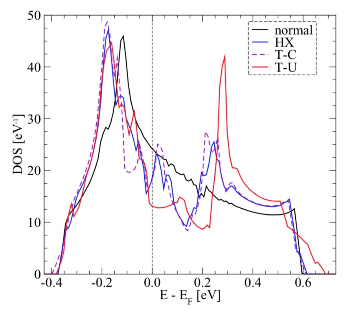
With reference to Fig. 10, the DOS of the main three CDW structures are compared to the DOS of the fully symmetric structure of pristine NbSe2. As presented elsewhere Calandra et al. (2009), for single-layers a single band crosses the Fermi level and extends from eV to eV. As the main contribution for this band come from Nb states, we refer to such band as Nb band. The CDW formation shifts the spectral weight from eV to eV and enhances it in the range () eV; the DOS peaks are aligned around eV, whereas the DOS peaks around eV are at different energy for different CDWs. The T-U CDW DOS features a depletion of spectral weight in correspondence of the Fermi level till eV and a trough at eV (which in fact precedes the peak at eV); the T-C CDW DOS has a trough at eV, a second one at Fermi level and a third one at eV; the HX CDW DOS has one trough at Fermi level and one at eV, being more similar to the T-C CDW DOS. The T-U differs from the other two also by a slightly larger band-width, whose tail reaches 0.7 eV. Overall, the CDW affects different energy ranges of the DOS both around the Fermi level and away from it, in agreement with the literature Shen et al. (2007); Calandra et al. (2009).
Appendix B Co adsorption
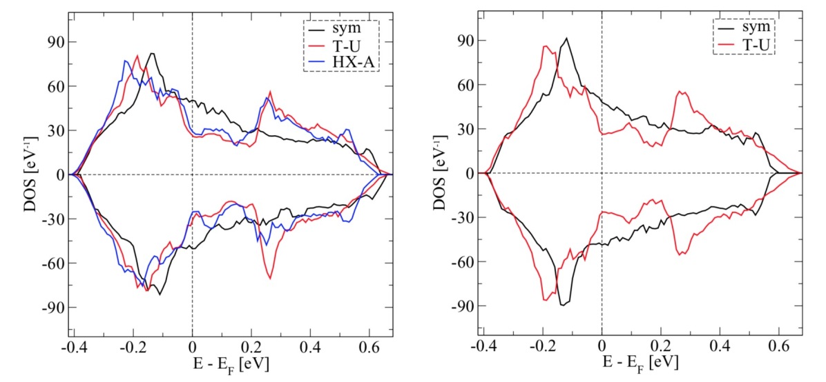
The DOS of symmetric and selected CDW structures obtained in the supercells, computed and analysed for CoNbSe2 and for KNbSe2 in supercells, is shown Fig. 13. By relaxing the MNbSe2 (M = Co, K) structures fixing the in-plane coordinates of the Nb and Se atoms, the symmetry of each structure was preserved; their relative DOS curves are labelled ‘sym’. The main features of the DOS of the T-U and HX CDWs are maintained with respect to the pristine CDWs: the peaks at eV and eV, and the depletion of states around Fermi level. However, the position of the peaks for the HX-A and T-U CDWs are now different in the case of Co adsorption; also, while the depletion of states in the pristine HX CDW is accompanied by peaks and troughs near Fermi level, the depletion of states in the HX-A CDW (i.e. with Co adsorbates) shows a profile in line with the T-U CDW. In summary, the effect of the CDW on the DOS slightly differs passing from the pristine case to the case with adsorbates, the states around Fermi level being the most affected ones.
With reference to Fig. 14, we analyse further details of the effect of Co/Mn adsorption on the CDW intensity, started with Fig. 6. The asymmetry of the FT plots, highlighted by computing the difference with the charge distribution in the pristine CDWs (T-U in the case of Fig. 6) is clearly due to the adsorbate, rather than the asymmetric nature of the CDW itself. In fact, Figs. 14 (a) and (b) show the FT of the charge densities of Co-adsorbed T-U and Mn-adsorbed T-U minus pristine T-U - while Fig. 14 (c) shows the Mn HX-S minus pristine T-U for comparison with the figure in the main text. The effect of Co adsorption and Mn adsorption on the CDW peaks is somehow opposite to each others: Co adsorption suppresses the CDW at , while enhancing it along the lines ; Mn adsorption suppresses the CDW at , enhancing it only at small values of . The asymmetry of the charge distribution of T-U suggests that such asymmetry is still reduced even for low concentrations of Co/Mn, when the energy competition starts to turn in favour of the T-U CDW.
A single Co adsorbed on NbSe2, with a concentration of 1 atom over 81 unit cells (a replica), was studied in order to assess how fast the energy order changes to recover that of pristine system. Four solutions were found within 0.4 meV/f.u, see Fig. 15; such small difference in energy makes them accessible by thermal fluctuations. The structure of the HX solutions shows some similarities to the case with higher adsorbate coverage. Among the low energy solutions, the T-C CDW was found with some mixing with HX and T-U, see Figs. 15 (a), (c) and (d). The T-U solutions are closer in energy to the ground state solution HX-A (0.3 - 0.4 meV/f.u.), whereas other mixed structures are found at higher energy, Figs. 15 (b) and (d), respectively.
The direct space charge distributions of the lowest energy HX solution and the first T-U solution are shown in Figs. 16 (a) and (b), corresponding to the structures shown in Fig. 15 (a) and (b); the HX solution shows characteristic patches of the T-C and HX CDWs, following the structural modulation and confirming the tendency for these two CDW to mix together upon Co adsorption; in fact, patches as represented in Fig. 1 are found in the supercell. The charge distribution of the T-U solution looks almost identical to that in the supercell, including the reduced symmetry, which is likely due to unidirectional local structural distortions driven by the Co electronic degree of freedom.
Finally, the energetic stability of CDWs in CoNbSe2 was also used to estimate how small changes of and affect the results presented in this manuscript. Several DFT+U calculations were performed for the supercell, sampling in the range eV and in the range eV. We found that the values reported in Table 2 are independent from the chosen Coulomb interaction parameters. The only exception is the calculation for eV and eV, when the HX-A CDW ends up in a different solution (minimum), much higher in energy, while the other two CDWs keep their energetic arrangement.
Appendix C Magnetic density
The comparison between magnetic couplings within the Nb band in the two cases of Co adsorption and Mn adsorption has been discussed in the main text. The actual magnetic moments (i.e. involving all states up to Fermi level) of Co, Mn and their respective underlying Nb atoms are , , and , respectively. In summary, the Co and Mn magnetic moments in the Nb bands are inverted with respect to the total magnetic moments, while the underlying Nb magnetic moments do not change sign, remaining positive in the case of Co adsorption and negative in the case of Mn adsorption.
References
- Novoselov et al. (2005) K. S. Novoselov, D. Jiang, F. Schedin, T. J. Booth, V. V. Khotkevich, S. V. Morozov, and A. K. Geim, Proc. Natl. Acad. Sci. 102, 10451 (2005).
- Xu et al. (2013) M. Xu, T. Liang, M. Shi, and H. Chen, Chem. Rev. 113, 3766 (2013).
- Choi et al. (2017) W. Choi, N. Choudhary, G. H. Han, J. Park, D. Akinwande, and Y. H. Lee, Materials Today 20, 116 (2017).
- Butler et al. (2013) S. Z. Butler, S. M. Hollen, L. Cao, Y. Cui, J. A. Gupta, H. R. Gutiérrez, T. F. Heinz, S. S. Hong, J. Huang, A. F. Ismach, E. Johnston-Halperin, M. Kuno, V. V. Plashnitsa, R. D. Robinson, R. S. Ruoff, S. Salahuddin, J. Shan, L. Shi, M. G. Spencer, M. Terrones, W. Windl, and J. E. Goldberger, ACS Nano 7, 2898 (2013).
- Geim and Grigorieva (2013) A. K. Geim and I. V. Grigorieva, Nature 499, 419 (2013).
- Novoselov et al. (2016) K. S. Novoselov, A. Mishchenko, A. Carvalho, and A. H. Castro Neto, Science 353 (2016).
- Splendiani et al. (2010) A. Splendiani, L. Sun, Y. Zhang, T. Li, J. Kim, C.-Y. Chim, G. Galli, and F. Wang, Nano Letters 10, 1271 (2010).
- Mak et al. (2010) K. F. Mak, C. Lee, J. Hone, J. Shan, and T. F. Heinz, Phys. Rev. Lett. 105, 136805 (2010).
- Kuc et al. (2011) A. Kuc, N. Zibouche, and T. Heine, Phys. Rev. B 83, 245213 (2011).
- Wang et al. (2012) Q. H. Wang, K. Kalantar-Zadeh, A. Kis, J. N. Coleman, and M. S. Strano, Nat Nano 7, 699 (2012).
- Chhowalla et al. (2013) M. Chhowalla, H. S. Shin, G. Eda, L.-J. Li, K. P. Loh, and H. Zhang, Nat. Chem. 5, 263 (2013).
- Frindt (1972) R. F. Frindt, Phys. Rev. Lett. 28, 299 (1972).
- Wilson et al. (2001) J. A. Wilson, F. J. D. Salvo, and S. Mahajan, Advances in Physics 50, 1171 (2001).
- Gong et al. (2017) Z. R. Gong, W. Z. Luo, Z. F. Jiang, and H. C. Fu, Sci. Rep. 7, 42390 EP (2017).
- Qi et al. (2016) Y. Qi, P. G. Naumov, M. N. Ali, C. R. Rajamathi, W. Schnelle, O. Barkalov, M. Hanfland, S.-C. Wu, C. Shekhar, Y. Sun, V. Süß, M. Schmidt, U. Schwarz, E. Pippel, P. Werner, R. Hillebrand, T. Förster, E. Kampert, S. Parkin, R. J. Cava, C. Felser, B. Yan, and S. A. Medvedev, Nat. Commun. 7, 11038 EP (2016).
- Lu et al. (2015) J. M. Lu, O. Zheliuk, I. Leermakers, N. F. Q. Yuan, U. Zeitler, K. T. Law, and J. T. Ye, Science (2015).
- Xi et al. (2015) X. Xi, L. Zhao, Z. Wang, H. Berger, L. Forró, J. Shan, and K. F. Mak, Nat Nano 10, 765 (2015).
- Xi et al. (2016a) X. Xi, Z. Wang, W. Zhao, J.-H. Park, K. T. Law, H. Berger, L. Forró, J. Shan, and K. F. Mak, Nat. Phys. 12, 139 EP (2016a).
- Ugeda et al. (2016) M. M. Ugeda, A. J. Bradley, Y. Zhang, S. Onishi, Y. Chen, W. Ruan, C. Ojeda-Aristizabal, H. Ryu, M. T. Edmonds, H.-Z. Tsai, A. Riss, S.-K. Mo, D. Lee, A. Zettl, Z. Hussain, Z.-X. Shen, and M. F. Crommie, Nat. Phys. 12, 92 (2016).
- Xi et al. (2016b) X. Xi, H. Berger, L. Forró, J. Shan, and K. F. Mak, Phys. Rev. Lett. 117, 106801 (2016b).
- Zhu et al. (2016) X. Zhu, Y. Guo, H. Cheng, J. Dai, X. An, J. Zhao, K. Tian, S. Wei, X. Cheng Zeng, C. Wu, and Y. Xie, Nat. Commun. 7, 11210 EP (2016).
- Bevolo and Shanks (1974) A. J. Bevolo and H. R. Shanks, J. Appl. Phys. 45, 4644 (1974).
- Corcoran et al. (1994) R. Corcoran, P. Meeson, Y. Onuki, P. A. Probst, M. Springford, K. Takita, H. Harima, G. Y. Guo, and B. L. Gyorffy, Journal of Physics: Condensed Matter 6, 4479 (1994).
- Wilson et al. (1974) J. A. Wilson, F. J. Di Salvo, and S. Mahajan, Phys. Rev. Lett. 32, 882 (1974).
- Moncton et al. (1975) D. E. Moncton, J. D. Axe, and F. J. DiSalvo, Phys. Rev. Lett. 34, 734 (1975).
- Revolinsky et al. (1965) E. Revolinsky, G. A. Spiering, and B. D. J., J. Phys. Chem. Solids 26, 1029 (1965).
- Rahn et al. (2012) D. J. Rahn, S. Hellmann, M. Kalläne, C. Sohrt, T. K. Kim, L. Kipp, and K. Rossnagel, Phys. Rev. B 85, 224532 (2012).
- Castro Neto (2001) A. H. Castro Neto, Phys. Rev. Lett. 86, 4382 (2001).
- Galvis et al. (2018) J. A. Galvis, E. Herrera, C. Berthod, S. Vieira, I. Guillamón, and H. Suderow, Communications Physics 1, 30 (2018).
- Zheng et al. (2018) F. Zheng, Z. Zhou, X. Liu, and J. Feng, Phys. Rev. B 97, 081101 (2018).
- Arguello et al. (2014) C. J. Arguello, S. P. Chockalingam, E. P. Rosenthal, L. Zhao, C. Gutiérrez, J. H. Kang, W. C. Chung, R. M. Fernandes, S. Jia, A. J. Millis, R. J. Cava, and A. N. Pasupathy, Phys. Rev. B 89, 235115 (2014).
- Rice and Scott (1975) T. M. Rice and G. K. Scott, Phys. Rev. Lett. 35, 120 (1975).
- Liu et al. (1998) R. Liu, C. G. Olson, W. C. Tonjes, and R. F. Frindt, Phys. Rev. Lett. 80, 5762 (1998).
- Straub et al. (1999) T. Straub, T. Finteis, R. Claessen, P. Steiner, S. Hüfner, P. Blaha, C. S. Oglesby, and E. Bucher, Phys. Rev. Lett. 82, 4504 (1999).
- Inosov et al. (2008) D. S. Inosov, V. B. Zabolotnyy, D. V. Evtushinsky, A. A. Kordyuk, B. Büchner, R. Follath, H. Berger, and S. V. Borisenko, New J. Phys. 10, 125027 (2008).
- Rossnagel et al. (2001) K. Rossnagel, O. Seifarth, L. Kipp, M. Skibowski, D. Voß, P. Krüger, A. Mazur, and J. Pollmann, Phys. Rev. B 64, 235119 (2001).
- Rossnagel and Smith (2007) K. Rossnagel and N. V. Smith, Phys. Rev. B 76, 073102 (2007).
- Johannes et al. (2006) M. D. Johannes, I. I. Mazin, and C. A. Howells, Phys. Rev. B 73, 205102 (2006).
- Johannes and Mazin (2008) M. D. Johannes and I. I. Mazin, Phys. Rev. B 77, 165135 (2008).
- Calandra et al. (2009) M. Calandra, I. I. Mazin, and F. Mauri, Phys. Rev. B 80, 241108 (2009).
- Valla et al. (2004) T. Valla, A. V. Fedorov, P. D. Johnson, P.-A. Glans, C. McGuinness, K. E. Smith, E. Y. Andrei, and H. Berger, Phys. Rev. Lett. 92, 086401 (2004).
- Zhu et al. (2015) X. Zhu, Y. Cao, J. Zhang, E. W. Plummer, and J. Guo, Proc. Natl. Acad. Sci. 112, 2367 (2015).
- Arguello et al. (2015) C. J. Arguello, E. P. Rosenthal, E. F. Andrade, W. Jin, P. C. Yeh, N. Zaki, S. Jia, R. J. Cava, R. M. Fernandes, A. J. Millis, T. Valla, R. M. Osgood, and A. N. Pasupathy, Phys. Rev. Lett. 114, 037001 (2015).
- Kotov et al. (2012) V. N. Kotov, B. Uchoa, V. M. Pereira, F. Guinea, and A. H. Castro Neto, Rev. Mod. Phys. 84, 1067 (2012).
- Guinea et al. (2014) F. Guinea, M. I. Katsnelson, and T. O. Wehling, Annalen der Physik 526, A81 (2014).
- Mak et al. (2012) K. F. Mak, K. He, C. Lee, G. H. Lee, J. Hone, T. F. Heinz, and J. Shan, Nat. Mater. 12, 207 EP (2012).
- Skripov and Stepanov (1985) A. Skripov and A. Stepanov, Solid State Commun. 53, 469 (1985).
- Malliakas and Kanatzidis (2013) C. D. Malliakas and M. G. Kanatzidis, J. Am. Chem. Soc. 135, 1719 (2013).
- Ángel Silva-Guillén et al. (2016) J. Ángel Silva-Guillén, P. Ordejón, F. Guinea, and E. Canadell, 2D Materials 3, 035028 (2016).
- Chatterjee et al. (2015) U. Chatterjee, J. Zhao, M. Iavarone, R. Di Capua, J. P. Castellan, G. Karapetrov, C. D. Malliakas, M. G. Kanatzidis, H. Claus, J. P. C. Ruff, F. Weber, J. van Wezel, J. C. Campuzano, R. Osborn, M. Randeria, N. Trivedi, M. R. Norman, and S. Rosenkranz, Nat. Commun. 6, 6313 EP (2015).
- Lian et al. (2017) C.-S. Lian, C. Si, J. Wu, and W. Duan, Phys. Rev. B 96, 235426 (2017).
- Fang et al. (2018) A. Fang, C. Adamo, S. Jia, R. J. Cava, S.-C. Wu, C. Felser, and A. Kapitulnik, Sci. Adv. 4 (2018).
- Soumyanarayanana et al. (2013) A. Soumyanarayanana, M. M. Yee, H. Yang, v. W. Jasper, D. J. Rahn, K. Rossnagel, E. W. Hudson, M. R. Norman, and J. E. Hoffman, Proc. Natl. Acad. Sci. 110 (2013).
- Cho et al. (2018) K. Cho, M. Konczykowski, S. Teknowijoyo, M. A. Tanatar, J. Guss, P. B. Gartin, J. M. Wilde, A. Kreyssig, R. J. McQueeney, A. I. Goldman, V. Mishra, P. J. Hirschfeld, and R. Prozorov, Nat. Commun. 9, 2796 (2018).
- Blöchl (1994) P. E. Blöchl, Phys. Rev. B 50, 17953 (1994).
- Kresse and Joubert (1999) G. Kresse and D. Joubert, Phys. Rev. B 59, 1758 (1999).
- Perdew et al. (1996) J. P. Perdew, K. Burke, and M. Ernzerhof, Phys. Rev. Lett. 77, 3865 (1996).
- Perdew et al. (1997) J. P. Perdew, K. Burke, and M. Ernzerhof, Phys. Rev. Lett. 78, 1396 (1997).
- Wehling et al. (2011) T. O. Wehling, A. I. Lichtenstein, and M. I. Katsnelson, Phys. Rev. B 84, 235110 (2011).
- Liechtenstein et al. (1995) A. I. Liechtenstein, V. I. Anisimov, and J. Zaanen, Phys. Rev. B 52, R5467 (1995).
- Wilson and Yoffe (1969) J. Wilson and A. Yoffe, Advances in Physics 18, 193 (1969).
- Lian et al. (2018) C.-S. Lian, C. Si, and W. Duan, Nano Letters 18, 2924 (2018).
- Shen et al. (2007) D. W. Shen, B. P. Xie, J. F. Zhao, L. X. Yang, L. Fang, J. Shi, R. H. He, D. H. Lu, H. H. Wen, and D. L. Feng, Phys. Rev. Lett. 99, 216404 (2007).
- Wei et al. (2017) X. Wei, B. Zhao, J. Zhang, Y. Xue, Y. Li, and Z. Yang, Phys. Rev. B 95, 075419 (2017).
- Kezilebieke et al. (2018) S. Kezilebieke, M. Dvorak, T. Ojanen, and P. Liljeroth, Nano Letters 18, 2311 (2018).
- Zhou et al. (2012) Y. Zhou, Z. Wang, P. Yang, X. Zu, L. Yang, X. Sun, and F. Gao, ACS Nano 6, 9727 (2012).
- Gao et al. (2018) S. Gao, F. Flicker, R. Sankar, H. Zhao, Z. Ren, B. Rachmilowitz, S. Balachandar, F. Chou, K. S. Burch, Z. Wang, J. van Wezel, and I. Zeljkovic, Proc. Natl. Acad. Sci. (2018).