Hybrid -tight binding model for subbands and infrared intersubband optics in few-layer films of transition metal dichalcogenides: MoS2, MoSe2, WS2, and WSe2
Abstract
We present a density functional theory parametrized hybrid kp tight binding model for electronic properties of atomically thin films of transition-metal dichalcogenides, 2H- (=Mo, W; =S, Se). We use this model to analyze intersubband transitions in - and -doped films and predict the line shapes of the intersubband excitations, determined by the subband-dependent two-dimensional electron and hole masses, as well as excitation lifetimes due to emission and absorption of optical phonons. We find that the intersubband spectra of atomically thin films of the 2H- family with thicknesses of to layers densely cover the infrared spectral range of wavelengths between and . The detailed analysis presented in this paper shows that for thin -doped films, the electronic dispersion and spin-valley degeneracy of the lowest-energy subbands oscillate between odd and even number of layers, which may also offer interesting opportunities for quantum Hall effect studies in these systems.
I Introduction
The 2H- transition metal dichalcogenide compounds (=Mo, W; =S, Se) are layered materials, where chalcogens and metal atoms form covalent bonds within two-dimensional (2D) layers with hexagonal lattice structure, and neighboring layers couple weakly through electrical quadrupole and van der Waals interactions. This feature of chemical bonding makes atomically thin films of sufficiently stable for extensive experimental studies aimed at their implementation in various optoelectronic devices Jariwala et al. (2014); Choi et al. (2017); Zhao et al. (2018). In those recent studies, the closest attention has been paid to the inter-band optical properties of the monolayer transition-metal dichalcogenide (TMD) crystals Wang et al. (2012); Liu et al. (2015); Mak and Shan (2016); Wurstbauer et al. (2017), due to their direct band gap Mak et al. (2010), valley-spin coupling Aivazian et al. (2015); MacNeill et al. (2015); Zhu et al. (2014), and long spin and valley memory of photo-excited carriers Yang et al. (2015), spiced up by the Berry curvature effects for electrons and excitons in these two-dimensional semiconductors Yu et al. (2014); Gunlycke and Tseng (2016). This is because in monolayer , and the valence and conduction band edges both appear at the Brillouin zone (BZ) corners and , where the electronic Bloch states carry intrinsic angular momentum.
Thicker crystals of 2H- quickly lose the direct band gap property upon increasing the film thickness to two or three layers Cheiwchanchamnangij and Lambrecht (2012); Cappelluti et al. (2013); Debbichi et al. (2014); Padilha et al. (2014); Chang et al. (2014); Fang et al. (2015); Bradley et al. (2015); Sun et al. (2016). Density functional theory (DFT) of few-layer transition metal dichalcogenides predicts Padilha et al. (2014); Fang et al. (2015) that for holes the band edge relocates to the point, whereas for electrons it appears at six points situated somewhere near the points at the middle of each segment (see inset in Fig. 1). This has been demonstrated by studies of Shubnikov–de Haas oscillations in -doped Pisoni et al. (2017). While the indirect character of few-layer TMD band structures suppresses their inter-band photo response, the multiplicity of subbands () at the conduction and valence band edges of the -layer crystal, open a new avenue for optical studies of atomically thin TMD films.
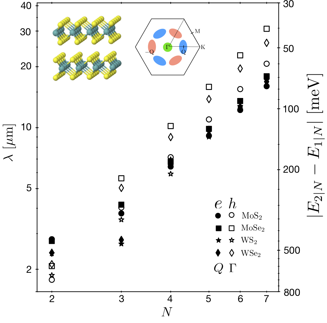
Here, we analyze theoretically intersubband transitions in few-layer and , and show that the absorption/emission spectra of the primary transitions in - and -doped crystals (Fig. 1) densely cover the infrared (IR) spectrum down to the far-infrared range (FIR) of photon energies. The analysis of subband properties of few-layer 2H- presented in this paper is based on the hybrid kp theory tight-binding model (HkpTB) approach, recently applied to the description of multilayer films of post-transitional-metal chalcogenides (such as and ) Magorrian et al. (2016); Bandurin et al. (2016). This approach consists of minimal theory Hamiltonians for 2H- monolayers Kormányos et al. (2013, 2015), supplemented by a expansion of the interlayer hopping near the relevant point (here, or ) in the BZ, with all parameters fitted to DFT calculated few-layer dispersions, and dispersions in bulk crystals.
First, in Section II we describe the lattice structure and discuss symmetries of few-layer 2D crystals of 2H-, especially the difference between films with odd and even numbers of layers and the corresponding degeneracies in their band structures. The DFT-parametrized HkpTB models for few-layer TMDs are formulated in Sections III and IV for the valence band edge (holes) near the point and for conduction band (electrons) near the points, respectively.
In the case of -doped films, our models predict a multi-valley subband structure with two valley triads connected by time-reversal symmetry, each consisting of three valleys related by rotations. We find that the lowest-energy subbands alternate between spin-split and spin-degenerate with number of layers , consequence of the mirror and full inversion symmetries of films with odd and even , respectively. These band structure features open a variety of new possibilities for studies of quantum Hall physics in multi-layer TMD films.
We calculate subband energies, dispersions, and wave functions of electron/hole subbands in -layer crystals of all four 2H- compounds, and optical oscillator strengths for radiative intersubband transitions. In particular, we take into account - and -type doping using a self-consistent analysis of charge and potential distributions across the film. Then, we analyze the inelastic broadening due to optical phonon emission, and the resulting spectral line shapes of IR/FIR absorption by - and -doped 2H- films. We find that the intersubband relaxation rates, determined by electron-phonon interactions, are much slower (one to two orders of magnitude) than the intra-subband relaxation in the same materials Danovich et al. (2017); Kozawa et al. (2014), and also these are an order of magnitude slower than intersubband relaxation of electrons and holes in III-V semiconductor quantum wells Unuma et al. (2003). Also, in Section III.2 we show that the difference between the two-dimensional masses and of electrons and holes in consecutive subbands leads to an additional temperature-dependent broadening of the intersubband transitions, , which appears to be the dominant intrinsic broadening effect for the IR/FIR absorption by 2H- films at room temperature.
II Multilayers of hexagonal transition metal dichalcogenides: overview
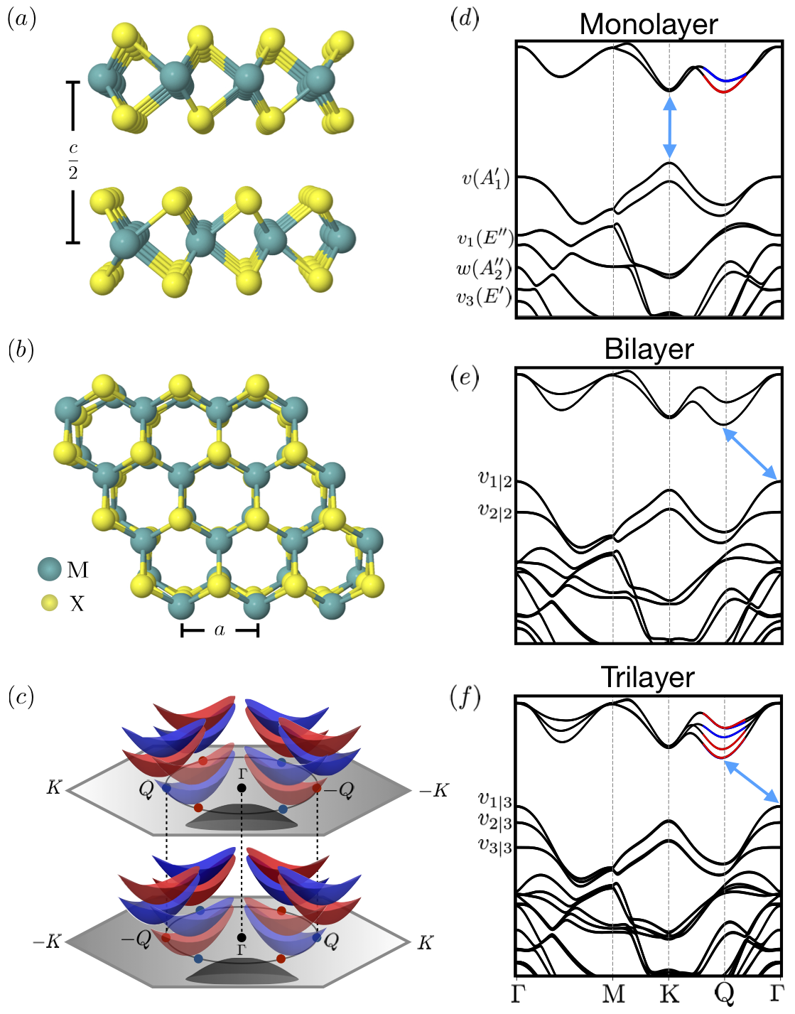
The lattice structure of monolayer TMDs contains two hexagonal sublattices of metal and chalcogen atoms in its unit cell, as shown in Fig. 2(b). The chalcogens form two sublayers, one above and one below the metal sublayer, forming a trigonal prismatic structure with the metal atom connected to three chalcogens above and below. The monolayer point-group symmetry is , consisting of rotations, in-plane mirror reflections, and out-of-plane mirror reflections. The most common bulk allotrope for these transition-metal dichalcogenides has 2H stacking Mattheiss (1973), built by adding subsequent layers rotated by with respect to the center of the hexagon, resulting in a structure where the chalcogen atoms from one layer are directly above or below metal atoms in the other layer [see Figs. 2(a) and 2(b)]. The interlayer distance , with the out-of-plane lattice constant, is shown in Fig. 2(a), and Fig. 2(b) shows the in-plane lattice constant . The resulting 3D layered crystal has a bipartite structure with two monolayers in the unit cell, belonging to the space group .
Multilayer TMDs with an even number of layers belong to the point group , which contains spatial inversion ( but lacks out-of-plane mirror symmetry. The combination of spatial inversion and time-reversal symmetry prescribed at zero magnetic field results in a constraint on the spin splitting of the electronic states for even number of layers, , where is the spin projection quantum number, such that all states throughout the BZ must be spin degenerate. Similarly to the monolayer case, multilayer films with an odd number of layers belong to the point group , which contains the mirror symmetry but lacks spatial inversion symmetry. Therefore, is a good quantum number for which spin degeneracy (present in films with even number of layers) can be lifted by spin-orbit (SO) coupling. While the SO splitting is absent for bands based on and orbitals at the point, it is substantial near the points, leading to the alternation of subband properties. That is, the subbands are spin degenerate for even numbers of layers, resulting in a six-fold degeneracy of dispersion along the line. For odd number of layers, subband spectra are three-fold degenerate, but with .
In Figs. 2(d)–(f) we show how the DFT calculated band structure of , representative of all four TMDs, evolves from monolayer to trilayer Cheiwchanchamnangij and Lambrecht (2012); Debbichi et al. (2014); Padilha et al. (2014); Chang et al. (2014); Fang et al. (2015); Bradley et al. (2015); Sun et al. (2016) (DFT band structures of all four TMDs can be found in Ref. sup ). The DFT calculations were performed using a plane-wave basis within the local density approximation (LDA), with the quantum espresso Giannozzi et al. (2009) plane-wave self-consistent field (PWSCF) ab initio package. We considered the Perdew-Zunger exchange correlation scheme Perdew and Zunger (1981), with fully-relativistic norm-conserving pseudo-potentials, including non-collinear corrections. Pseudopotentials for Mo, W, S, and Se atoms were generated using atomic code ld1.x of the PWSCF package Dal Corso (2014). The cutoff energy in the plane-wave expansion was set to , and the BZ sampling of electronic states was approximated using a Monkhorst-Pack uniform grid of for all structures Monkhorst and Pack (1976). We adopted a Methfessel-Paxton smearing Methfessel and Paxton (1989) of and set the total energy convergence to less than in all calculations. Spin-orbit coupling was included in all electronic band structure calculations. To eliminate spurious interactions between adjacent supercells, a vacuum buffer space was inserted in the out-of-plane direction. We used experimental values for the interlayer separations Böker et al. (2001); Al-Hilli and Evans (1972); Wieting (1970); Hicks (1964) and LDA optimized in-plane lattice constants for all four TMDs sup .
Using WS2 as an example, Fig. 2 illustrates that a monolayer has a direct band gap at the point of the BZ. The mirror symmetry and lack of inversion symmetry result in SO-split conduction and valence bands, classified by their spin projection quantum number [Fig. 2(d)]. The large SO splitting at the valence band (VB) point and conduction band (CB) point results from their metal and orbital compositions. This is in contrast to the CB point, which is primarily made of metal orbitals, resulting in weaker SO splitting Kormányos et al. (2015); Liu et al. (2015). In a 2H- bilayer, the combination of spatial inversion and time reversal symmetry forbids SO splitting, resulting in two spin-degenerate subbands (four bands in total) in the CB and VB, split by the interlayer coupling [Fig. 2(e)]. Additionally, the interlayer coupling shifts the band edges to the point (VB) and in the vicinity of the point (CB), making indirect gap semiconductors.
In the trilayer 2H-, the valence and conduction band edges remain at the and near points. As shown in Fig. 2(f), the CB subbands are split by SO coupling at the point due to the lack of spatial inversion symmetry in the case of odd numbers of layers. The resulting spectrum consists of two SO-split subbands in the middle, and two pairs of nearly spin-degenerate subbands above and below (see Appendix C for details). For the valence subbands, however, SO splitting is forbidden exactly at the point, due to it being its own time reversal counterpart, resulting in three nearly spin degenerate subbands [exact degeneracy for even , and spin-splitting for odd ]. This trend, which consists of the alternation of SO-split (for odd ) and spin-degenerate (for even ) subbands persists for TMD films with a larger number of layers, and all the same features are present in the spectra of all four 2H- shown in Ref. sup . Finally, we note that the in-plane (2D) carrier dispersions in different subbands (both on the VB and CB sides) are different, which affects the intersubband absorption line shapes, as we discuss in Secs. III and IV.
III Hole subbands in -doped few-layer TMDs
Figure 2(d) shows the monolayer valence bands relevant for the multilayer description, based on symmetry and energy considerations. The and valence bands are non-degenerate at the point, with the band composed of the metal orbital and chalcogen orbitals, whereas the band is composed of metal and chalcogen orbitals. Bands and belong to two-dimensional irreducible representations (Irreps), with the band composed of chalcogen and metal orbitals, and the -band formed by chalcogen and metal orbitals Kormányos et al. (2013, 2015); Liu et al. (2015). In the multilayer case, the and bands strongly repel as the band gets closer in energy to the band. The and bands, on the other hand, are weakly split with a narrow spread due to their orbital characters, and are pushed downwards relative to the band edge. The two-dimensional Irreps of and allow their coupling with the VB being only through SO interactions (see Appendix B). These features involving the symmetry, orbital composition, and proximity of the valence bands, supported by our numerical calculations, indicate that the VB is most strongly hybridized with the band, while the other valence bands , , provide corrections in second-order perturbation theory to the model parameters through the action of SO coupling (see Appendix B). Additionally, as pointed out in Sec. II, in two-dimensional 2H- crystals the CB and VB are almost spin degenerate at the point, despite the fact that atomic SO coupling in TMD compounds is strong. Therefore, to describe the valence subbands at the point, we construct a spinless two-band model including the and bands, fitting the band parameters and interlayer hopping terms to the DFT calculated band structure, where SO coupling is included implicitly. As indicated in Fig. 2(d), these bands belong to the and Irreps of the group of the point Kormányos et al. (2013, 2015), respectively. Therefore, bands and are, respectively, even and odd under transformations, and do not mix in the monolayer case. However, in multilayers, band mixing across consecutive layers is allowed by symmetry.

III.1 HkpTB for the -point valence band edge
The monolayer dispersions of the valence bands and , are described by isotropic parabolic dispersions with band-dependent effective masses
| (1) |
To construct the multilayer Hamiltonian, we include symmetry-constrained interlayer couplings, given to lowest orders in by
| (2) |
where and are interlayer intra-band hopping terms, and couples different bands in two consecutive layers.
The multilayer Hamiltonian is given by
| (3) |
where we have defined . and annihilate (create) a band- electron with spin projection and in-plane wave vector in the odd and even layers of the unit cell, respectively. Additional model parameters include the on-site energy corrections and , and -dependent corrections of the form , for the and bands, respectively, which take into account both the pseudo-interlayer potentials, as well as the spin-flip-induced interband-interlayer hopping (Appendix B). For odd the system has complete unit cells and a truncated last unit cell , where and are the floor and ceiling functions, respectively. This case is considered in Eq. (3) through the Heaviside function , which removes the operators when is odd. The minus sign in the last row of Eq. (3) for the interband interlayer hoppings () is due to the opposite parity under of the and bands, described in Sec. III. Finally, we include on-site potential energy shifts , for , to take into account the effects of an electric field applied along the TMD film’s axis. Under experimental conditions, such an electric field may originate from a negative back gate, which in addition dopes the system with a finite hole density . This density is related to the potential profile as Magorrian et al. (2018),
| (4) |
where is the (positive) fundamental charge, is the interlayer distance, and is the electrostatically induced density of holes in layer , such that . The factor of 2 in the second equation comes from the spin degeneracy at the point. The potential profile and hole density must be determined self-consistently to satisfy Eq. (4).
Setting , we obtain the model parameters in Eq. (3) for each 2H- by fitting the results of numerical diagonalization of Eq. (3) to DFT calculations of bulk and few-layer dispersions. For example, the DFT bulk dispersion of is shown in Fig. 3 for the cut through the 3D BZ. The solid lines in Fig. 3 correspond to the bands of the bipartite Bloch Hamiltonian
| (5) |
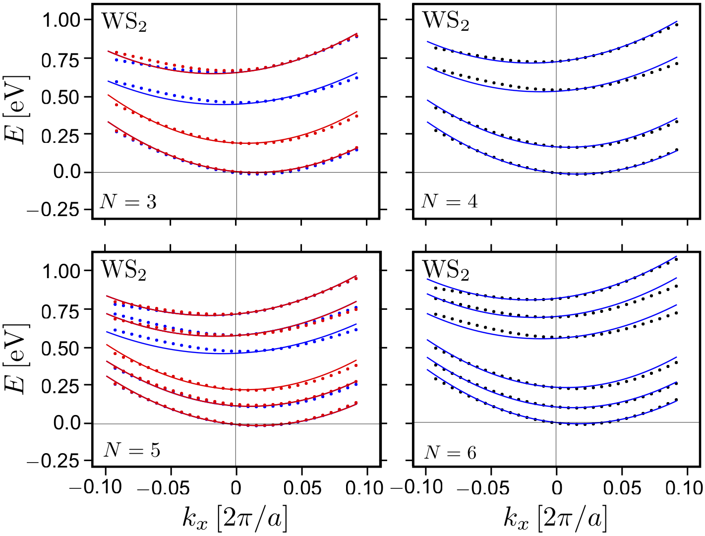
obtained from the model Eq. (3). Equation (5) is written in the basis of the and bands of layers one and two of the bulk 2H crystal unit cell. The fitted parameters for the four TMDs are given in Tables 1 and 2, and sample comparisons between the HkpTB model and DFT results for WS2, representative of all four TMDs, are shown in Fig. 4. Detailed comparisons for few-layer films of all four materials are available in Ref. sup .
Noting that the bulk VB edge is located at the point (Fig. 3), the dispersion near the band edge can be obtained from Eq. (5) as
| (6) |
where the bulk parameters are given in terms of the HkpTB model parameters,
| (7a) | |||
| is the out-of-plane bulk effective mass, with the interlayer distance and the bulk gap between the topmost and lowest bands at the point. | |||
| (7b) | |||
| is the in-plane bulk effective mass, and | |||
| (7c) | |||
is an anisotropic non-linearity factor. These parameter values, obtained by fitting to DFT calculations, can be found in Table 1.
| 1.75 | 3.726 | 0.304 | |
| 1.04 | 0.693 | -5.24 | |
| 1.56 | 5.575 | 0.505 | |
| 1.42 | 0.786 | -5.99 | |
| 2.08 | 2.885 | 0.353 | |
| 0.840 | 0.615 | -5.86 | |
| 1.81 | 3.420 | 0.760 | |
| 1.08 | 0.700 | -5.45 |
| -0.333 | 0.592 | 1.744 | 2.684 | |
| 0.432 | -1.206 | -62.18 | -41.43 | |
| -0.351 | 6.770 | |||
| -0.307 | 0.657 | 1.830 | 2.626 | |
| 0.453 | -1.140 | -29.13 | -10.85 | |
| -0.261 | 2.736 | |||
| -0.322 | 0.574 | 1.718 | 3.205 | |
| 0.404 | -1.226 | -36.98 | -48.89 | |
| -0.614 | 5.834 | |||
| -0.291 | 0.649 | 1.814 | -1.382 | |
| 0.4309 | -0.049 | -25.27 | -69.93 | |
| -0.519 | 0.192 |
Then, the subband energies and dispersions in TMD films with can be analyzed by quantizing hole states with dispersions described by Eq. (6) in a slab of thickness . When doing so, one has to complement Eq. (6) with the general Dirichlet-Neumann boundary condition for the standing waves of holes at both film surfaces
| (8) |
where the correspond to the top and bottom layers, respectively, and is a dimensionless parameter. Assuming a solution of the form , one finds from Eq. (8) that in Eq. (6) obeys
| (9) |
where the integer is the subband index. For large number of layers and for subbands near the band edge, , and , so that we can approximate
| (10) |
leading to the subband energies and dispersions
| (11) |
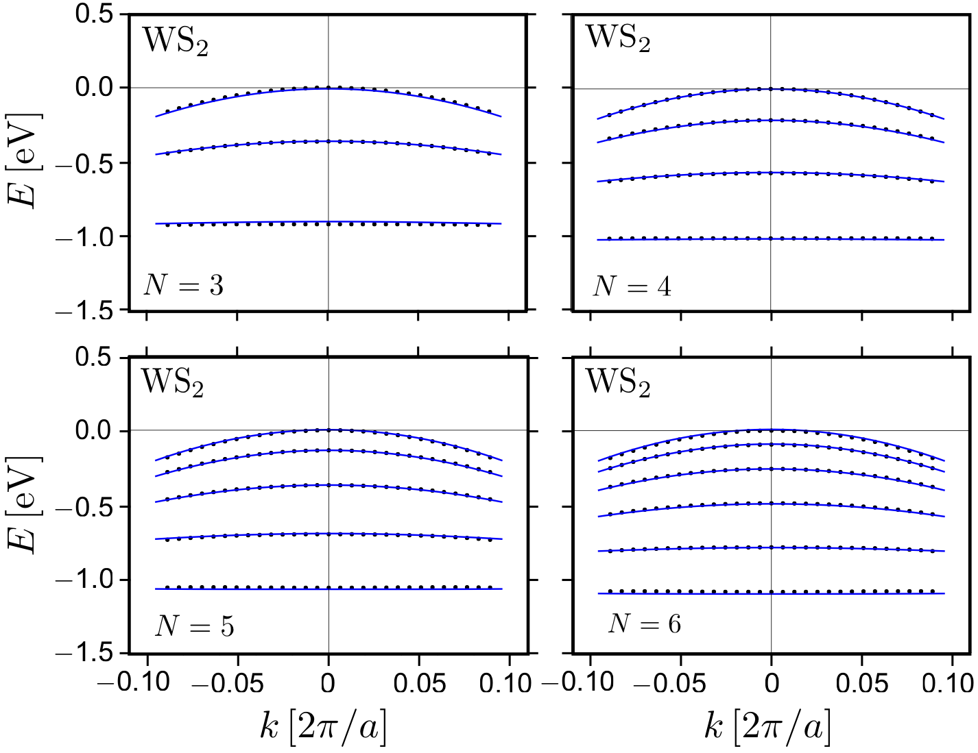
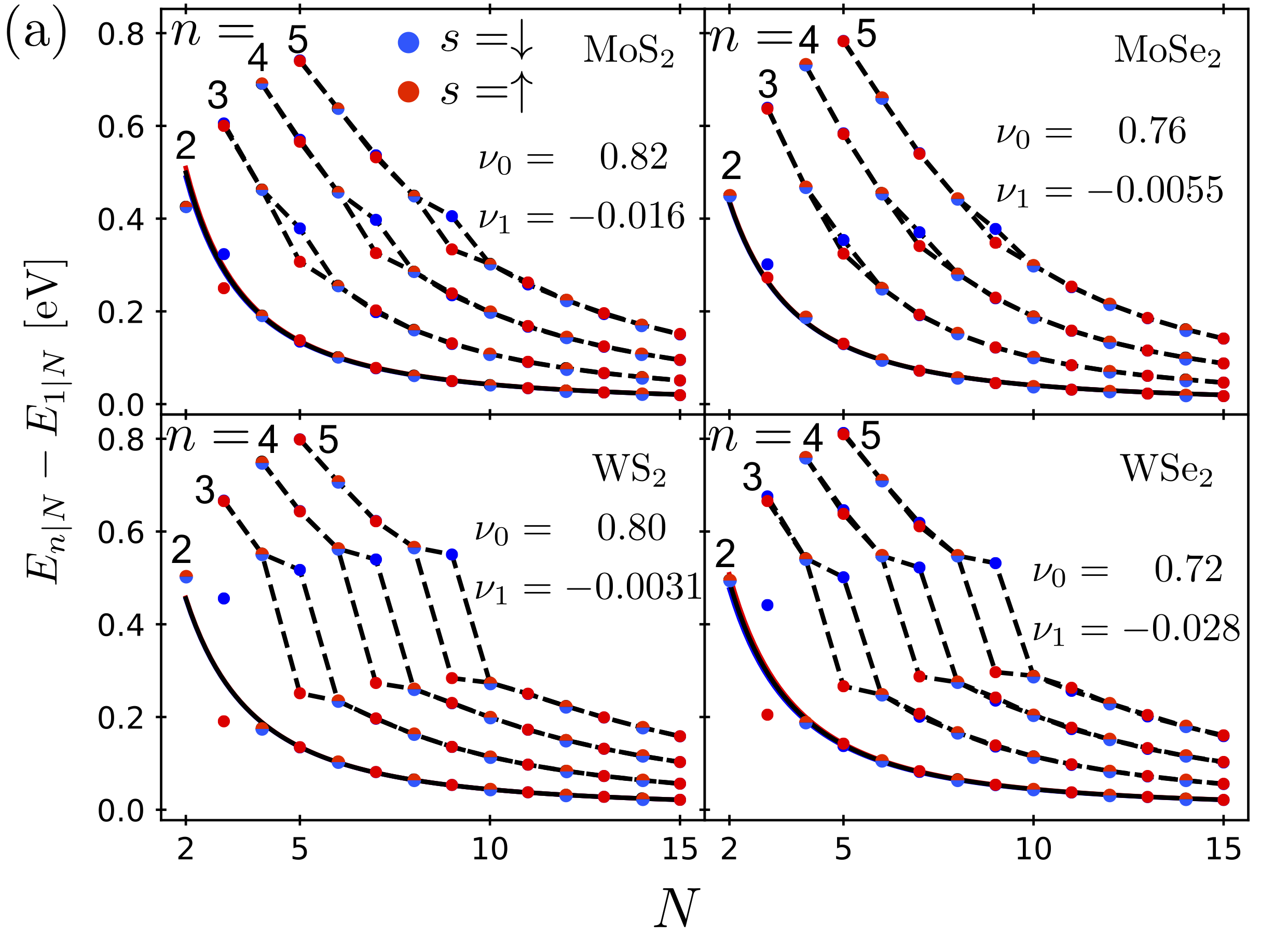
The large- asymptotics of the separation between the lowest two subbands, , was used to determine the value of the boundary parameter for holes in each TMD, resulting in for and , for , and for , using the dispersions and lowest intersubband splittings shown in Figs. 4 and 5(a). The good agreement between the full HkpTB model and the asymptotic analysis shown in Fig. 5(a) enables us to describe the main intersubband transition in -doped -layer 2H- as
| (12) |
Furthermore, the hole subband effective masses
| (13) |
obtained from Eq. (11), describe well the subband dependence of the in-plane masses, as seen in Fig. 5(a).
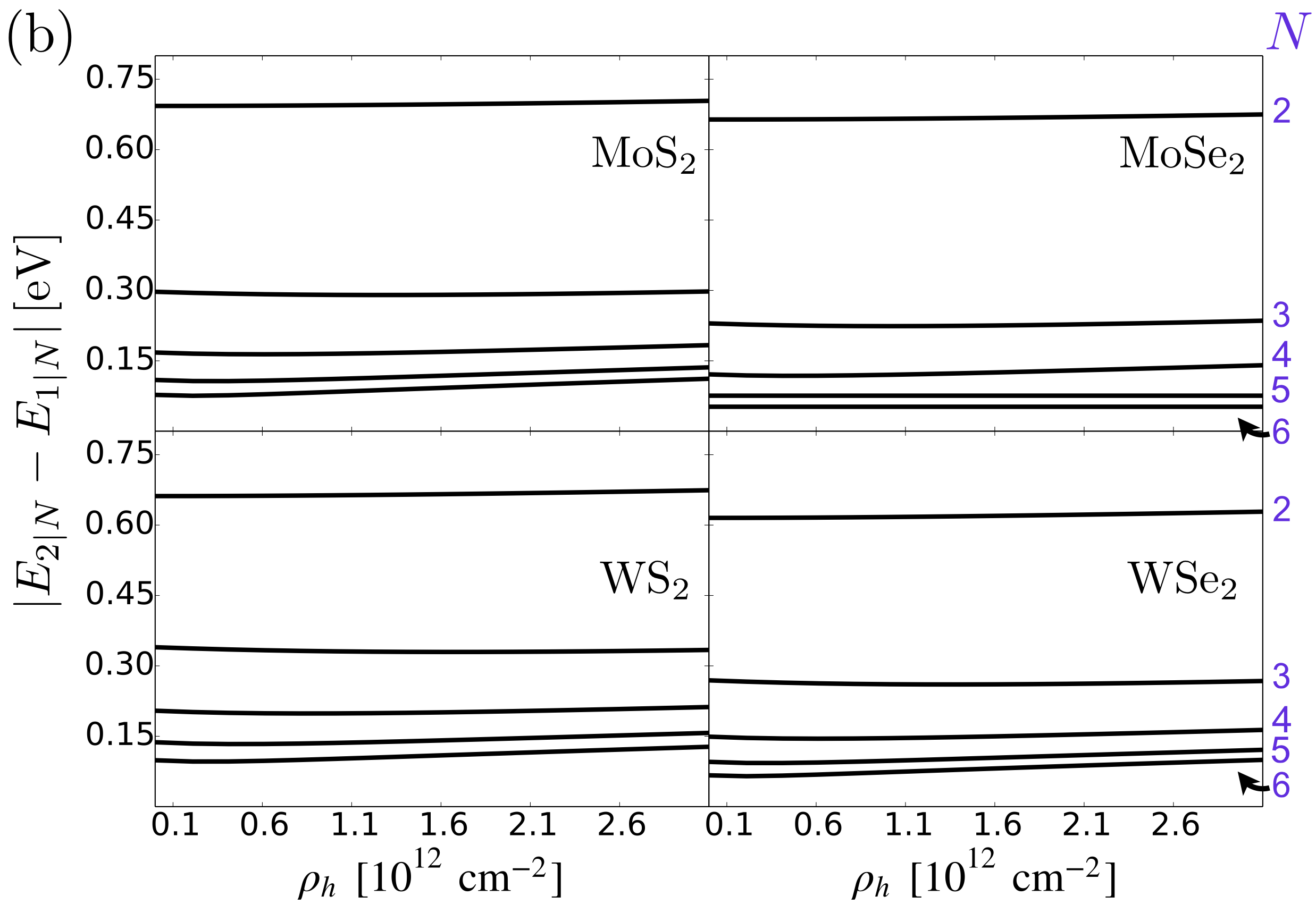
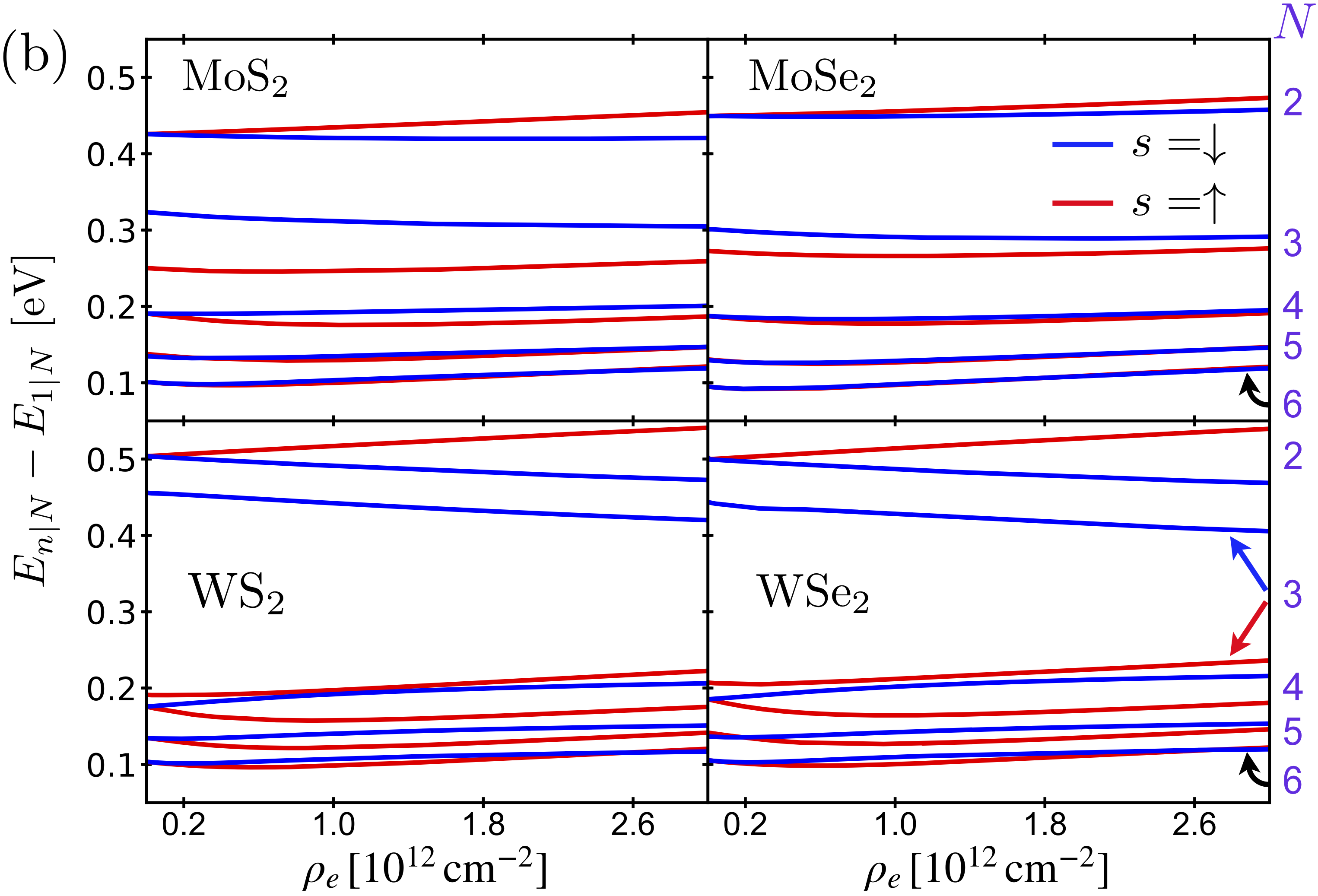
Fig. 5(b) shows the effects of a doping-induced potential profile in the film on the first subband transition energy , as a function of the total gate-induced hole density . Results are shown for all four TMDs with film thicknesses of to 6 layers, up to moderate doping levels. Following a slight decrease for weak doping, the transition energies grow monotonically, but with only a weak blue shift.

III.2 Selection rules for intersubband transitions, and dispersion-induced line broadening
Next, we use the model developed above for the description of hole subbands to study intersubband optical transitions, electron-phonon relaxation, and absorption line shapes of IR/FIR light.
The optical transition amplitude between two given subbands and is determined by the out-of-plane dipole moment
| (14) |
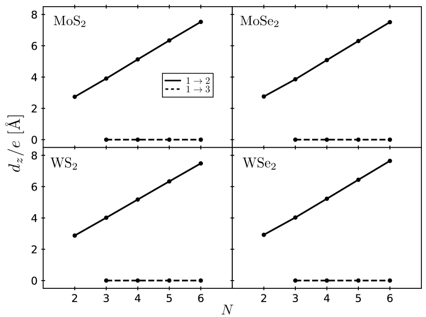
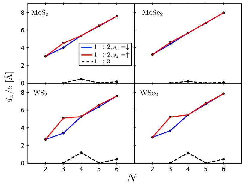
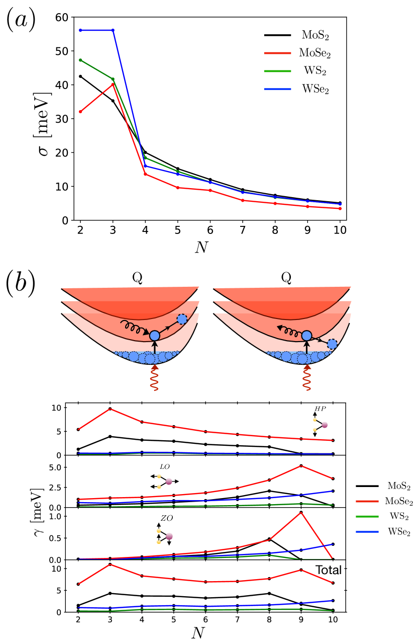
where is the total number of layers, denotes the coordinate of layer , and are the components of the subband eigenstate. The calculated dipole moment matrix element for the first two intersubband transitions is plotted in Fig. 6 as a function of the number of layers. The selection rules for intersubband transitions driven by out-of-plane polarized light are determined by the odd parity of under both spatial inversion and mirror reflection (). The subband states for even and odd number of layers also have a definite parity under spatial inversion and mirror reflection, respectively, due to the crystal’s symmetry. Therefore, intersubband transitions between same parity subbands are forbidden, as shown in Fig. 6 for the first two intersubband transitions. All this makes the transition the dominant feature in the IR/FIR absorption by thin TMD films.
The intersubband absorption line shape is affected by the difference between the effective masses of subbands and . The lighter in-plane hole mass in the initial state ( subband) as compared to the final state ( subband) spreads the absorption spectrum toward lower energies. Heavy -doping of the TMD film or Boltzmann distribution of the holes in the case of light -doping, sets the lower limit for the line width of the absorption line, which we call the density of states (DOS) broadening
| (15) |
Here, is the Boltzmann constant, is the temperature, and are the effective masses of the first and second subbands. This limit for the line width is illustrated in Fig. 7(a) for -layer 2H- at room temperature. We note here that DOS broadening is similar to the inhomogeneous broadening, in the sense that it can be overcome by placing the TMD film inside an optical resonator that would select intersubband modes with particular values of in-plane momentum .
III.3 Broadening due to electron-phonon intra- and intersubband relaxation
In contrast to the elastic DOS broadening, phonon-induced intra- and intersubband relaxation broaden the absorption line in a way that cannot be avoided by a clever choice of the electromagnetic environment. Below we consider emission and absorption of homopolar (HP), longitudinal (LO) and out-of-plane (ZO) optical phonons, which we assume to be dispersionless. This choice is motivated by the fact that these are the strongest coupled modes in TMDs, as established by earlier studies Danovich et al. (2017); Sohier et al. (2016). Also, we take phonon modes of few-layer films as independent and degenerate. This approximation is justified by the fact that splittings due to hybridization between layers are much smaller than the monolayer phonon frequency Froehlicher et al. (2015).
The hole-phonon couplings for a phonon in mode , or ZO in layer , interacting with a hole in layer , are given by (see Appendices D and E)
| (16a) | |||
| (16b) | |||
| (16c) |
where denotes the corresponding phonon frequency; is the mass density of the material; is the deformation potential in the valence band; is the unit cell area; and are the total unit-cell mass and reduced mass of the metal and two chalcogens, respectively; and are the in-plane and out-of-plane Born effective charges, respectively; and is the screening length in the material. The various parameters taken from Refs. Danovich et al., 2017; Sohier et al., 2016; Jin et al., 2014; Gu and Yang, 2014 are given in Table 3.
| [meV] | [meV] | [meV] | [g/cm2] | [eV/Å] | [eV/Å] | ||||||
|---|---|---|---|---|---|---|---|---|---|---|---|
| MoS2 | 51 | 49 | 59 | 3.5 | 7.1 | 1.08 | 0.1 | 41 | 0.24 | 8.65 | |
| MoSe2 | 30 | 37 | 44 | 3.8 | 7.8 | 1.8 | 0.15 | 52 | 0.249 | 9.37 | |
| WS2 | 52 | 44 | 55 | 1.5 | 3.4 | 0.47 | 0.07 | 38 | 0.29 | 8.65 | |
| WSe2 | 31 | 31 | 39 | 2.2 | 2.7 | 1.08 | 0.12 | 45 | 0.25 | 9.37 |
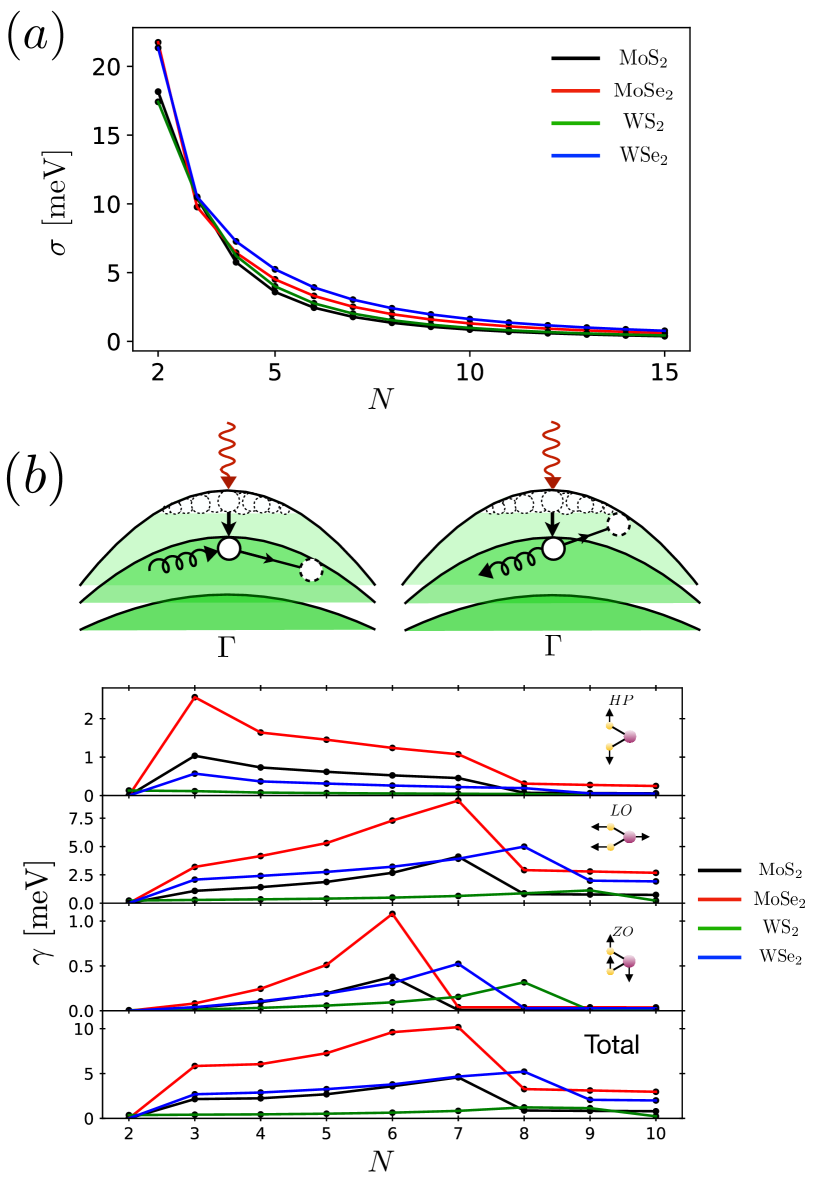
The phonon-induced broadening is determined by the lifetime of the hole in the excited subband state, which includes contributions from intersubband relaxation due to emission (low and high temperature) and intrasubband absorption (high temperature) [Fig. 7(b)]. We note that intrasubband emission contributions are thermally activated, since they require carriers to be thermally excited to energies higher than the corresponding phonon energy. The typical energy of thermally distributed carriers at room temperature is meV, whereas the phonon energies are of order – meV (Table 3), making this process irrelevant. Similarly, the process involving intersubband absorption from the second subband to the third is suppressed by the larger intersubband spacings, as compared to the phonon energies and the first intersubband spacings for , and therefore will not be considered.
The phonon-induced broadening is accounted for by
| (17) |
where the sums are over the phonon modes , the phonon wave vector , and the layer number . are the components of the subband eigenstate on layer in band , and is the Bose-Einstein distribution for a phonon in mode at temperature . The first term in curly brackets describes intersubband phonon emission, whereas the second term describes intrasubband phonon absorption.
The resulting phonon-induced broadenings at room temperature are shown in Fig. 7(b). The main contribution comes from intersubband relaxation, with intrasubband absorption suppressed by the phonon occupation number. The intersubband LO phonon contribution dominates the broadening due to the strong coupling attributed to the large in-plane Born effective charge, and the long-range nature of the coupling. The reduced broadening for is due to the large intersubband spacing, which suppresses intersubband relaxation, and the fact that the second subband is almost flat, which suppresses intrasubband absorption. The peaks in the broadenings for certain numbers of layers correspond to near resonances between the phonon energies and the intersubband spacings. Phonon broadening is seen to be most detrimental for in particular, and in general for all TMDs with seven or eight layers. Beyond this number of layers, the phonon energies become larger than the intersubband spacings, thus preventing intersubband relaxation, however, intrasubband absorption is still present and dominates for . Finally, we note that the broadening values are found to be smaller than those observed in III-V quantum wells Unuma et al. (2003), implying a weaker detrimental effect on the absorption/emission line shape in these materials.
III.4 Room-temperature absorption spectrum in -doped TMD films
The cumulative effect of inelastic (e-ph) and elastic (DOS) broadening of the intersubband absorption spectra of lightly -doped TMD films is described by
| (18) |
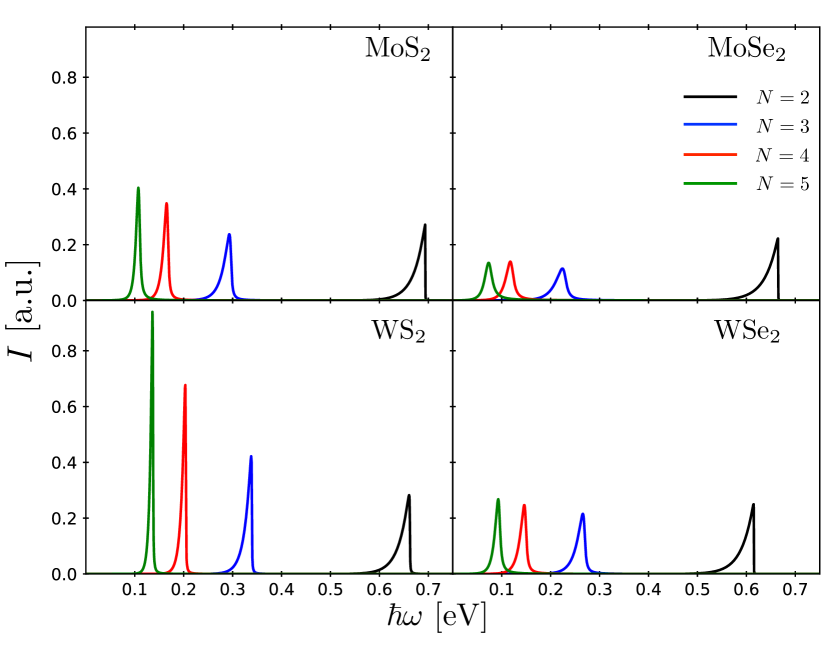
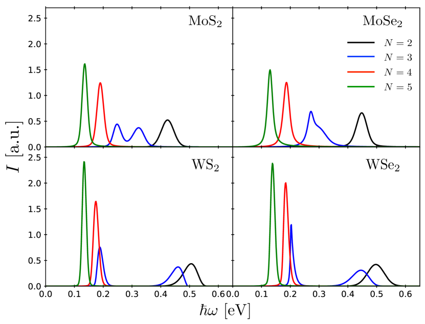
where is the Fermi function for hole occupation in the lowest subband corresponding to hole density , and temperature (we assume that all higher-energy hole subbands are empty). The resulting absorption spectra at room temperature for the four TMDs with different number of layers are shown in Fig. 8. The spectra show the combination of DOS broadening, which produces a tail towards lower photon energies, with the phonon-induced broadening, most relevant for , which gives a small tail towards higher energies, making the lines more symmetric and reducing their amplitudes. The smaller phonon couplings in result in tall, narrow, and asymmetric line shapes, with intensity increasing with the number of layers, reflecting the growing dipole matrix element. This is in contrast to , where the larger phonon-induced broadening results in smaller and more symmetric peaks for .
IV Electron subbands in -doped few-layer TMDs
IV.1 HkpTB for the conduction band near the point
| 0.595 | 1.035 | 20.49 | 0.666 | 1.105 | 7.16 | 1.994 | 67.0 | |
| 0.525 | 0.550 | 0.735 | -3.90 | -7.94 | 0.0456 | -1.3 | ||
| 0.583 | 1.060 | 54.21 | 0.518 | 1.106 | 26.93 | 1.891 | 21.0 | |
| 0.500 | 0.510 | 0.760 | -4.65 | -4.26 | 0.0663 | 0.32 | ||
| 0.529 | 0.722 | 13.74 | 0.763 | 0.892 | -20.65 | 2.059 | 254 | |
| 0.510 | 0.528 | 0.596 | -4.30 | -4.12 | 0.0344 | 0.53 | ||
| 0.468 | 0.753 | 49.63 | 0.676 | 0.908 | 1.88 | 1.94 | 214 | |
| 0.466 | 0.479 | 0.608 | -4.19 | -5.80 | 0.0599 | -0.9 |
The conduction band edges in monolayer MoS2, MoSe2, WS2, and WSe2 are located at the points, but accompanied by local dispersion minima that appear near the six inequivalent points , and , where , and is the midpoint between and ( is the lattice constant). For a given value of , there are three valleys connected by rotations about the BZ center [Fig. 2(c)], such that we need only describe the dispersion near the two points , which are related by time reversal.
For spin projection , the monolayer dispersion near the valley is given by Kormányos et al. (2015)
| (19) |
where and are effective masses; is a constant energy shift; is the spin-orbit splitting between the spin-up and down band edges; and is the band-edge momentum relative to the valley along the axis. From time-reversal symmetry we obtain the dispersion for the opposite valley as , which requires () and .
As described in Sec. II, the 2H-stacked bilayer consists of subsequent layers rotated by with respect to each other. In reciprocal space, this means that a conduction-band state of spin projection and momentum of the first layer will hybridize with its in-plane inversion partner of spin and momentum in the second one [Fig. 2(c)]. The multilayer Hamiltonian for the conduction subbands about is given by
| (20) |
where and annihilate (create) electrons of spin projection , in-plane wave vector and valley quantum number , on the odd and even layers of the bulk unit cell. The alternation of spin indices and hopping terms are a result of 2H stacking. The model is parameterized by the terms in given in Eq. (21), the interlayer pseudo-potential , implemented as an on-site energy shift at the boundary layers, and the next-nearest-neighbor hopping included to improve the fitting to DFT bands. The interlayer hopping has the form (see Appendix A)
| (21) |
up to second order in the in-plane crystal momentum. Given the lack of symmetry for even , the spin projection is, strictly speaking, not a good quantum number, and spin mixing is allowed. This is discussed in Appendix A. However, using an expansion about the point in our DFT results shows that spin mixing is much weaker Gibertini et al. (2014) than , and can be neglected. We also found to be several orders of magnitude smaller than ; as a result, we consider to be real.
Finally, in the last term of Eq. (20) we take into account electrostatic doping effects through the layer-dependent potential energy () Magorrian et al. (2018):
| (22) |
Here, is the electron (number) density induced in layer belonging to the spin- subbands in valley . The factor of 3 in the second equation comes from the valley degeneracy, which is preserved even in the presence of an out-of-plane electric field.
| 0.203 | 0.213 | 0.0419 | |
| 12.7 | -0.662 | 8.90 | |
| 0.215 | 0.180 | -0.145 | |
| 20.5 | -0.447 | -4.29 | |
| 0.210 | 0.233 | -0.123 | |
| 5.24 | -0.864 | -3.95 | |
| 0.211 | 0.209 | 0.231 | |
| 9.54 | -0.797 | 4.21 |
In the bulk limit, and in the absence of external electric fields (), we have the bipartite Hamiltonian
| (23) |
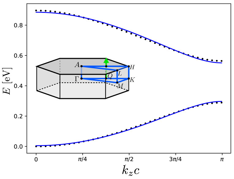
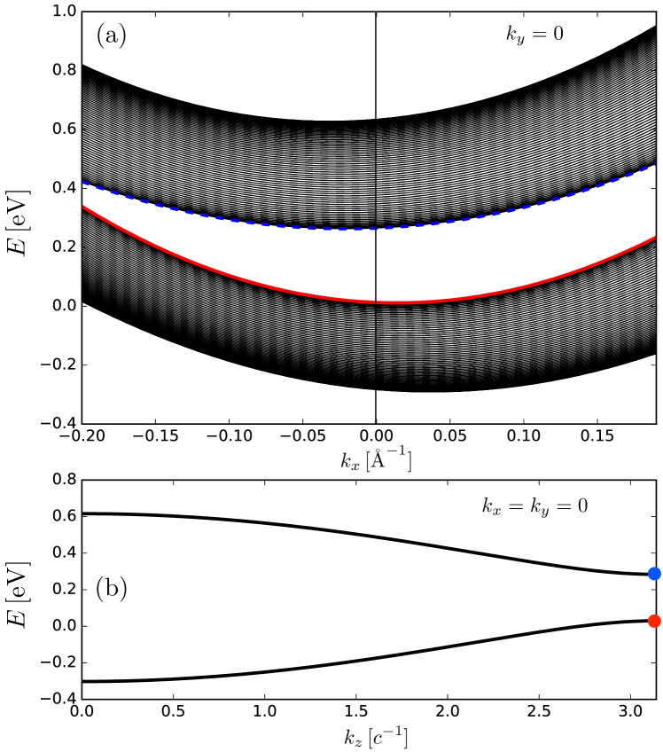
where is the -dependent monolayer spin-orbit splitting for wave vector measured relative to the point; and ( to ) are Pauli matrices acting on the spin and layer degrees of freedom, respectively, and and are the identity in their corresponding subspaces. The model parameters for the four TMDs were fitted to the DFT-calculated monolayer and 3D bulk dispersions, and are presented in Tables 4 and 5. A sample bulk fitting is shown in Fig. 9 for , along the path defined by ( point) and , with the solid line corresponding to the model Eq. (23). A sample comparison between our HkpTB model to DFT results for WS2 few-layer structures, representative of all four TMDs, is shown in Fig. 10. Detailed comparisons for few-layer films of all four materials are available in Ref. sup .
As discussed in Sec. II, the global symmetry alternation between for odd , and spatial inversion symmetry for even , results in the striking qualitative differences between the cases with even and odd number of layers in Fig. 10. The two-fold spin degeneracy observed for even is a consequence of spatial inversion and time reversal symmetry, resulting in . By contrast, mirror symmetry for odd makes a good quantum number, while the lack of inversion symmetry allows for spin-orbit splitting. Notice also that the two middle spin-split subbands remain fixed for all odd values of , while the rest of the bands are nearly spin-degenerate. As discussed in Appendix C, these features can be traced back to the SO splitting in the monolayer case, and the particular form of Hamiltonians for odd .
Expanding the lowest eigenvalue of Eq. (23) for valley about , corresponding to the bulk conduction band edge (Fig. 9), the dispersion can be written as
| (24) |
where is the out-of-plane bulk effective mass; are the in-plane effective masses in the and directions, respectively; are anisotropic non-linearity factors; and account for the band minimum offset from the point along the direction; and is a constant energy shift. These constants are related to our HkpTB model parameters through the expressions [see Eq. (19)]
| (25a) | |||
| (25b) | |||
| (25c) | |||
| (25d) | |||
| (25e) | |||
| (25f) | |||
| (25g) | |||
| (25h) |
Similarly to the subbands on the valence-band side (Sec. III), the conduction subbands in TMD films with can be analyzed by quantizing the electron states in a slab of finite thickness , with dispersions described by Eq. (24). However, note that the coefficients of Eqs. (25a)–(25h) are independent of spin projection and valley, and thus not representative of the odd case. This is a consequence of the explicit inversion symmetry of the bulk model (23). Nonetheless, the SO splitting resulting from the lack of inversion symmetry and the presence of symmetry in a system with odd , can be introduced through the TMD quantum well boundary conditions.
The unit cell for 2H crystals contains two layers, which below we label A and B [see Eq. (20)]. For odd , inversion symmetry is broken in opposite ways for the two layers in the unit cell, given that, as discussed in Sec. I, they are rotated by with respect to each other. This results in different boundary conditions for electrons at a given termination of the TMD film, depending on whether the final layer is of type A or B. This generalizes the boundary conditions used for the valence band at the point [Eq. (8)] to
| (26a) | |||
| for the boundary at when the film terminates on an A layer, and | |||
| (26b) | |||
when the final layer at position is of type B. Here, are dimensionless parameters. This results in spin- and valley-dependent quantization conditions
| (27) |
where gives for even and for odd . Overall, the low-energy spectrum of a thin film has the form
| (28) |
where the subband in-plane effective masses in the directions are
| (29a) | |||
| and the momentum offset from the point is given by | |||
| (29b) | |||
As in the monolayer case, the low-energy subband dispersions described by Eq. (28) near the six valleys at BZ points , , and , can be divided into two triads related by time-reversal symmetry, with quantum numbers . The three valleys for a given are connected by rotations, as sketched in the inset of Fig. 2. As a consequence, for odd number of layers, where inversion symmetry is broken and SO splitting is parameterized by , the spin and valley degrees of freedom of the bottom subband are locked, and the low-energy states have valley degeneracy of . Conversely, for even number of layers the bottom subbands are spin degenerate, giving a total degeneracy of . These large subband degeneracies and multi-valley structures, together with the anisotropic dispersions found within each valley, may have important implications for the transport and quantum Hall properties of -doped multilayer TMDs Wu et al. (2016).
Both inversion and symmetry are broken when an electric field is applied along the axis of the film, leading to a modulation of the spin splittings in the case of odd , and lifting of the spin degeneracy for even . As a first approximation, this effect can be introduced into the lowest subband dispersion by substituting
| (30) |
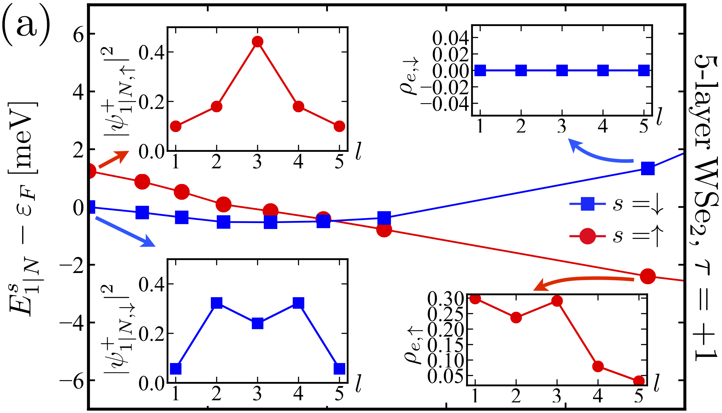
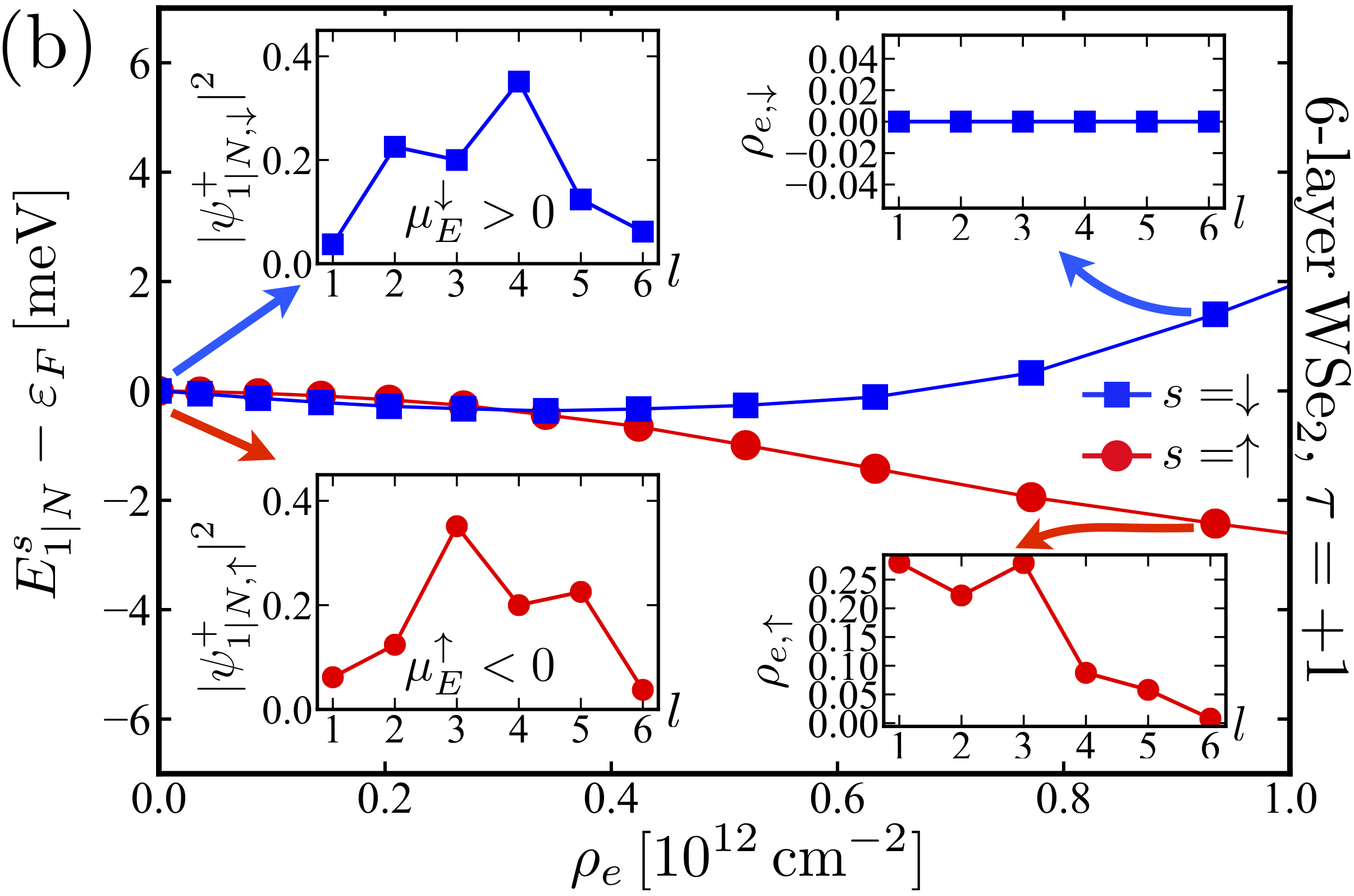
in Eq. (28) for , where is the total electron density induced by the field. These spin-dependent shifts of the band edges, abbreviated , parametrize the symmetry breaking by the potential profile. As an example, representative of all four TMDs, Figure 11 shows this splitting for the lowest conduction subband of five- and six-layer WSe2, in the case where the field is induced by a single positive back gate near layer one. The corresponding induced electron densities and potential profiles were determined self-consistently to satisfy Eq. (22), and chosen inside a range that is easily accessible to experiments.
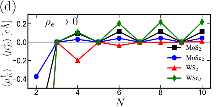
In the case of even we can interpret the spin-splitting strength in the weak doping regime in terms of the spatial charge distributions of the lowest-energy spin-up and -down subband states. The left insets in Fig. 11(b) show the spread of these two states along the film’s axis in the zero-doping limit (). The two distributions are asymmetric with respect to the middle of the film, and related to each other by a mirror operation, resulting in opposite electric dipole moments about the middle plane of the multilayer structure. The splitting in the zero-doping limit can be approximated as , where is the electric field in the direction. This is shown in Fig. 11(b) for electron densities between 0 and . This linear splitting contribution is weak: even at small doping, it is overcome by non-linear screening effects, which produce a large negative splitting [Fig. 11(c)] and quickly deplete the spin-down subband, as shown in the right insets of Fig. 11(b). For odd , where in the zero-doping limit the states of both spin band edges are symmetric about the middle layer of the film [see insets of Fig. 11(a)], spin splitting is determined entirely by non-linear effects. This analysis for the limit can be generalized to all even and odd values of for all four TMDs, as shown in Fig. 11(d), where we show that, in all four cases, the spin-resolved electric dipole moments alternate between finite and zero for even and odd , respectively. Also, note that according to Eq. (30), the sign of the spin splitting is inverted for opposite valleys.
IV.2 Intersubband transitions and dispersion-induced line broadening in -doped -layer TMDs
Numerically diagonalizing the HkpTB Hamiltonian in Eq. (20) with the parameters of Tables 4 and 5, we obtain the energy spacings between the first and next few subbands of TMD films shown in Fig. 12.
Using Eq. (28), we estimate the separation between the lowest two subbands of a given spin projection as
| (31) |
Similarly, we estimate the splitting between the lowest subbands of opposite spin as
| (32) |
We used Eqs. (31) and (32) to determine the boundary parameters and for each of the considered TMDs (MoS2: , MoSe2: , WS2: , WSe2: ). The results are shown with solid lines in Fig. 12. In the absence of an electric field, the energy splitting between the lowest two spin polarized transitions is of order few for the four TMDs. However, this splitting is enhanced by electron doping, as shown in Fig. 12(b) for two- to six-layer films of all four TMDs. For , the spin-up (-down) transition energy grows (decreases) linearly with the doping level for small electron densities. The opposite trend is found for to , where the spin-up subband transition appears at lower energy, and non-linear effects begin to appear already for low electron doping. We conclude that the electron doping level can be used as an additional tunable parameter to modify the energies and degeneracies of the lowest optical transitions in 2H-TMDs.
Next, we use the model developed above for electron subbands to study intersubband optical transitions, intersubband electron-phonon relaxation, and the intersubband absorption line shapes for IR/FIR light. As discussed in Sec. III.2, the optical transition amplitude between two given subbands is determined by the out-of-plane dipole moment
| (33) |
where is the total number of layers, denotes the coordinate of layer , and are the components of the subband eigenstate of spin projection and valley quantum number . The calculated dipole moment matrix element as a function of number of layers for the first two intersubband transitions is plotted in Fig. 13.
Similarly to the valence subbands case, optical transitions in films with odd number of layers are allowed only between states with opposite-parity subband indices, corresponding to opposite parity under transformation. The spin-orbit splitting present for odd results in a spin selection rule, allowing transitions only between subbands with the same out-of-plane spin projection . For even , where symmetry is absent, transitions between subbands with same-parity indices are allowed. This is in contrast to the VB at the point, and is a consequence of the multiple-valley structure of the CB, which makes it possible to form degenerate even and odd (under inversion) combinations of states, giving a finite dipole moment, as shown in Fig. 13 for the first two intersubband transitions, considering both spin-down and -up polarized subbands. This makes transition the dominant feature in the IR/FIR absorption by thin -doped TMD films.
Similarly to the holes in -doped TMDs, the line shape of the electron intersubband absorption in -doped films is also affected by the difference between the effective masses of subbands and . However, in contrast to the case of holes, for electrons the line shapes depend also on the relative in-plane wave vectors of the conduction subband minima, as well as the anisotropic subband dispersions. The resulting broadening for -layer 2H- films at room temperature, obtained numerically from the calculated line shapes, is shown in Fig. 14(a). Our calculations show that the aforementioned DOS broadening factors result in a typically larger broadening, which spreads the absorption spectrum towards both lower and higher energies from the main transition.
IV.3 Electron-phonon relaxation and room-temperature absorption spectra in -doped TMD films
The phonon-induced broadening for conduction subbands and , generated by intrasubband and intersubband relaxation, is accounted for by
| (34) |
where is the subband edge offset from the point of subband with spin projection , and are the electron-phonon couplings for the three phonon modes = HP, LO, and ZO given in Eq. (16), with replaced by for the HP phonon. The first term in Eq. (34) describes intersubband relaxation due to phonon emission, whereas the second describes intrasubband phonon absorption in the excited subband. The phonon induced broadening for the four TMDs obtained using the electron-phonon coupling parameters in Table 3 are shown in Fig. 14(b). The dominant contribution comes from intersubband relaxation due to HP and LO phonon modes, with a smaller contribution from the thermally suppressed intrasubband absorption. The large HP phonon deformation potential at the point, as compared to its value at the point Jin et al. (2014), in particular for and (see Table 3), results in a large contribution to the broadening. Additional differences between the phonon-induced broadenings for the conduction and valence subbands originate from the different intersubband spacings as a function of number of layers (Figs. 5 and 12), and different dispersions (Figs. 4 and 10). As in the valence subbands case, the phonon broadening is most significant for due to stronger electron-phonon coupling.
The absorption spectra of -doped TMD films calculated using Fermi’s golden rule, as in Eq. (18), and taking the discussions of Secs. IV.1, IV.2, and IV.3 into account, are shown in Fig. 15 for to layers. The predicted absorption spectra for the four TMDs are seen to be more symmetric than those for the holes, primarily due to the effect of different dispersions in consecutive subbands, here aggravated by the shifts and the BZ position of the subbands minima, in addition to the difference between the in-plane subband effective masses. The large SO splitting between the middle two subbands for results in two distinct lines, whereas for the spin-polarized subbands are nearly degenerate, resulting in the overlap of the two lines and giving a combined line with twice the amplitude.
V Conclusions
We have presented hybrid kp tight-binding models for the conduction and valence band edges of multilayer TMDs, capable of reproducing the rich low-energy subband dispersions, and allowing us to describe the intersubband optical transitions when coupled to out-of-plane polarized light. In particular, we find the following:
-
•
The subbands at the CB edge are found near the valleys of the Brillouin zone, whereas the valence band edge is found at the point. The main differences between the two sets of subbands are due to the significant spin-orbit splitting, multi-valley structure, and anisotropic dispersions of the conduction subbands, by contrast to the valence subbands. These differences manifest themselves in the absorption line shapes and additional selection rules, particularly for odd number of layers, where spin-orbit splitting is present.
-
•
The four studied TMDs were found to have main intersubband transition energies for the conduction and valence subbands, which densely cover the spectrum range of wavelengths from to ( to ), for to layers. This allows tailoring structures of a specific material, appropriate type of doping, and number of layers for a particular device application, from IR to the THz range.
-
•
Two contributions to the absorption line-shape broadening are identified. The first, broadening due to intersubband phonon relaxation, is found to produce a meV limit to the intersubband linewidth. This is in contrast to III-V quantum wells, where phonon broadening is found to be more damaging to the intersubband transition line quality factor Unuma et al. (2003). A second, elastic contribution to the line broadening caused by the different 2D masses of carriers in consecutive subbands yields a thermal broadening of the order of . Similarly to inhomogeneous broadening, this effect can be reduced by coupling the transition in the film to a standing wave of light in a high- resonator.
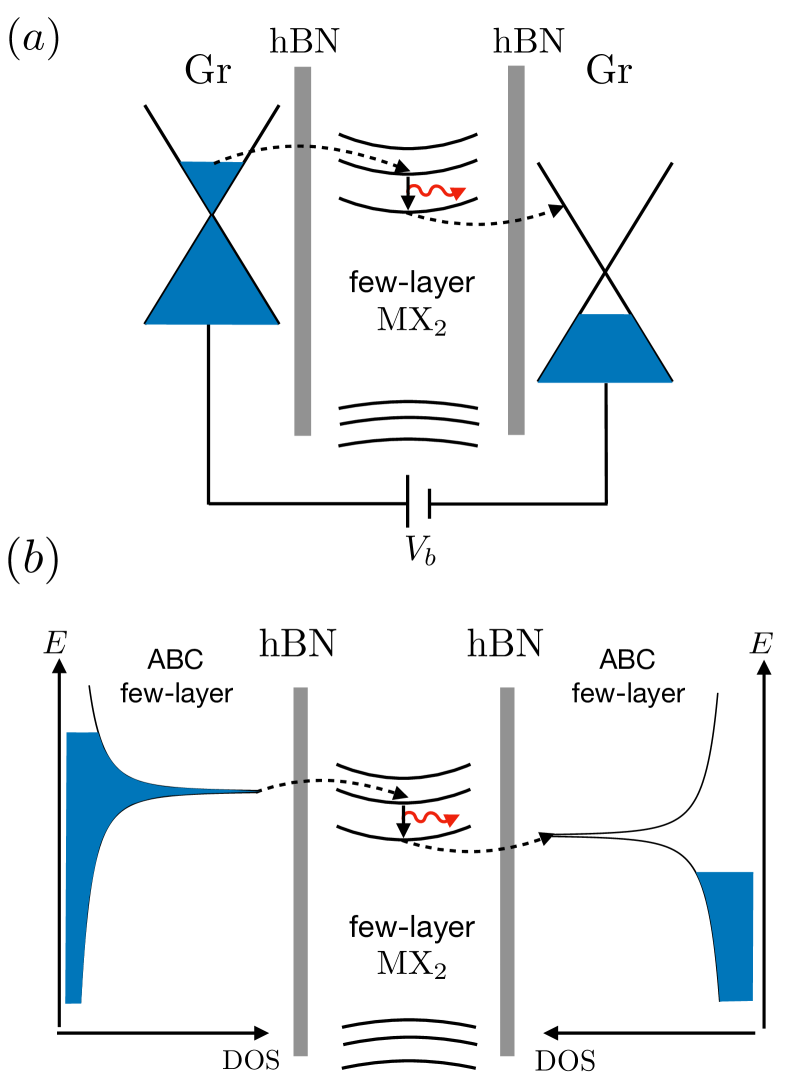
Finally, we propose a specific design of van der Waals multilayer structure utilizing the intersubband transitions in atomically-thin films of TMDs. The sketch in Fig. 16 depicts the band configuration of a few-layer transition-metal dichalcogenide film, encapsulated by hexagonal boron nitride (BN) and placed between two graphene electrodes. Applying a bias (and possibly also gate) voltage between the two electrodes results in a shift of the Dirac points relative to each other, and allows for the alignment of the Dirac point of the “top” graphene electrode with the lower-energy subband in the TMD, while keeping the Fermi level in graphene above the higher-energy subband. The carriers can then tunnel from the graphene electrode into the higher-energy subband. Once in the excited subband state, the carrier can undergo an intersubband transition, emitting light polarized in the out-of-plane direction, followed by tunneling to the second graphene electrode from the bottom subband state.
A potentially more favorable realization of the above process which avoids carrier loss directly from the second subband, or carrier tunneling into the bottom subband, involves using ABC-stacked few-layer graphene. The band structure of ABC few-layer graphene has a Van Hove singularity in its density of states at the edge between conduction and valence bands. Aligning the Van Hove singularities of two such electrodes with the second and first subbands, respectively, would enable one to achieve preferential injection and extraction of carriers into/from the TMD film, thus offering a new way to produce functional optical fiber cables.
The proposed “LEGO”-type design of IR/THz emitting materials has potential for implementation as part of a composite optical fiber, where the coupling to the out-of-plane polarized photon would be supported by the wave-guide mode.
Acknowledgements.
The authors acknowledge funding by the European Union’s Graphene Flagship Project, ERC Synergy Grant Hetero 2D, EPSRC Doctoral Training Centre, Graphene NOWNANO, and the Lloyd Register Foundation Nanotechnology grant, as well as support from the N8 Polaris service and the use of the ARCHER supercomputer (RAP Project e547) and the Tianhe-2 supercomputer (Guangzhou, China). The authors would like to thank F. Koppens, K. Novoselov, R. Gorbachev, M. Potemski, R. Curry, C. Kocabas, S. Magorrian and A. Ceferino for fruitful discussions.Appendix A Symmetry constraints for the bilayer Hamiltonians
For (bilayer), the Hamiltonian must be invariant under spatial inversion , mirror symmetry , and time reversal . For the conduction-band model about the point, this gives the conditions Bernevig and Hugues (2013)
| (35a) | |||
| (35b) | |||
| (35c) |
We have , and , where () are Pauli matrices acting on the layer (spin) subspace, and represents complex conjugation. As a result, the most general valley-spin structure for the bilayer Hamiltonian at the valley is
| (36) |
where the symmetry constraints (35a)-(35c) require that
| (37a) | |||
| (37b) | |||
| (37c) | |||
| (37d) | |||
| (37e) |
One can check that, for , Eq. (20) corresponds to , , and , and that these terms meet the symmetry requirements. Furthermore, we carried out fittings to DFT data using the additional spin-orbit terms and . The fittings give ; hence, we conclude that these terms can be neglected.
Appendix B Spin-orbit-coupling induced interband coupling at the point valence bands
Here, we analyze the role of spin-orbit coupling and coupling to distant bands in determining parameters for the valence-band HkpTB model.
The spin-orbit coupling is given by , where and are the orbital and spin angular momentum operators. This can also be written in terms of the ladder operators and as
| (39) |
where describe a spin flip with corresponding change in orbital angular momentum projection. These terms couple the and bands with the bands and [Fig. 2(d)], which in the absence of SO coupling are doubly degenerate. Band ( Irrep of ) has basis functions which are odd under (metal orbitals being the dominant component Kormányos et al. (2015), as well as chalcogen ). Band ( Irrep of ) has basis functions even under (metal orbitals and chalcogen ). Including SO coupling results in the splitting of these bands into new bands denoted by the orbital and spin angular momentum projections along , , and , corresponding to total angular momentum projections of and , respectively.
The -band belongs to the one-dimensional Irrep (even under , with metal dominant and chalcogen ), and has and . Similarly, the -band belongs to the one-dimensional Irrep, and is dominated by the odd (under ) chalcogen orbitals, giving two states with and .
Therefore, in the bilayer, where symmetry is broken, the and -bands can couple to and bands, with the appropriate spin-flip terms. In the second-order perturbation theory, this coupling produces corrections to the on-site energy
| (40) |
Note that these corrections are the same for both spin components of the or bands, with only one of the terms contributing for a given spin state.
An additional SO induced interband coupling with a spin-flip may be present in the multilayer case, affecting the interlayer coupling
| (41) |
where the pre-factor is related to the gradient of the interlayer pseudo-potential , and we defined . In contrast to the previous coupling, this coupling has a -dependence, which affects the dispersions. The coupling in Eq. (41) is odd under spatial inversion. Due to the 2H-stacked bilayer having spatial inversion symmetry, the coupling is non-zero only between different bands in the two layers. In second-order perturbation theory, we get a nominal redefinition of the 2D mass used in the HkpTB model, by adding the term
| (42) |
with a fitting parameter.
Appendix C Spin-split bands at the Brillouin zone edge for odd number of layers
The effective -point Hamiltonians for odd can be split into two decoupled blocks of different spin projection as , where the blocks have the alternating matrix form
| (43) |
and we have defined
| (44a) | |||
| (44b) |
Defining the even-dimensional matrix
| (45) |
the eigenvalues of (43) are given by a secular equation
| (46) |
Using the fact that , we can continue expanding Eq. (46) to obtain
| (47) |
which explicitly shows that is an overall factor, and thus is always an eigenvalue, regardless of the (odd) value of . For a given , the different quantum numbers give two spin-split monolayer dispersions about the () points, corresponding to the features observed in Fig. 10. The fact that this prediction is verified in the DFT band structures clearly confirms the validity of our hybrid model.
For large odd , nearly spin-degenerate bands grow denser on either side of the spin-split bands without crossing them, as shown in Fig. 17(a). The reason for this becomes clear when we take the bulk limit, and find that the spin-split states form the band edges around a central gap in the subband structure. This is shown in Fig. 17(b). Indeed, in the limit of large the Hamiltonian (43) corresponds to the bulk Hamiltonian at , since [see Eq. (23)].
Appendix D Electron-phonon coupling for LO phonon in multilayer system
In this appendix, we derive the expression used for the electron-phonon coupling with LO phonon in a multilayer system. As described in the text, we treat the LO phonon in each layer as independent and degenerate. However, in the LO phonon case, the generated electrostatic potential due LO phonon in one layer interacts with the electrons in all the other layers in the system, following similar steps as in Ref. [Kaasbjerg et al., 2012].
Within a monolayer, the LO phonon-induced in-plane polarization is given by its in-plane Fourier component,
| (48) |
where is the Born effective charge on the metal and chalcogens, is the unit-cell area, is the phonon-induced atomic displacement in the direction connecting the metal and chalcogens in the unit cell, with the reduced mass of the metal and chalcogens, the number of unit cells in the sample, and the LO phonon frequency. is the dielectric function characterizing the response of the material to the phonon induced electric field.
The induced charge density in the layer is given by , with the Fourier component
| (49) |
The potential resulting from the charge distribution is given by Poisson’s equation . Fourier-transforming in three dimensions gives,
| (50) |
where is the Fourier parameter in the direction. Inverse Fourier transforming in gives the dependence of the potential with in-plane Fourier component
| (51) |
The electron-phonon coupling for an electron localized in an isolated monolayer is given by . This form of the coupling is similar to the form derived in Refs. [Sohier et al., 2016; Danovich et al., 2017], where the polarizability of a two-dimensional dielectric was taken into account by the replacement , with the screening length in the material. For multilayer 2H-stacked TMDs, as the polarization in subsequent layers alternates in its sign, the resulting electrostatic potential also alternates in its sign.
Appendix E Electron-phonon coupling for ZO phonon in multilayer system
The atomic vibrations for the ZO optical phonon mode result in a polarization in the out-of-plane direction due to the opposite motions of the metal and two chalcogens, and the finite Born effective charges in the -direction. The interaction energy in the multilayer system between charges and phonon-induced out-of-plane polarizations in all layers is given by Ganchev et al. (2015)
| (52) |
where is the charge density on layer , is the out of plane polarization in layer caused by the ZO optical phonon, the interlayer separation, and we sum over all layer pairs. Fourier transforming the charge density and polarization in the in-plane momentum components gives
| (53) |
and similarly for the polarization. The interaction energy then takes the form,
| (54) |
Defining the new variables , , and integrating over gives ,
| (55) |
where in the last row we used , since the density is real. Carrying out the integration over gives
| (56) |
where the prime over the sum means that the summation excludes the term with . Quantizing the phonon polarization and the carrier density gives
| (57) |
where is the annihilation (creation) operator for an electron in state in layer , and is the annihilation (creation) operator for a phonon with in-plane wave vector . The phonon-induced polarization is given, similarly to the LO phonon case, by the Born effective charge and the phonon displacement.
The electron-phonon interaction Hamiltonian is then given by
| (58) |
References
- Jariwala et al. (2014) D. Jariwala, V. K. Sangwan, L. J. Lauhon, T. J. Marks, and M. C. Hersam, ACS Nano 8, 1102 (2014).
- Choi et al. (2017) W. Choi, N. Choudhary, G. H. Han, J. Park, D. Akinwande, and Y. H. Lee, Materials Today 20, 116 (2017).
- Zhao et al. (2018) Y. Zhao, W. Yu, and G. Ouyang, Journal of Physics D: Applied Physics 51, 015111 (2018).
- Wang et al. (2012) Q. H. Wang, K. Kalantar-Zadeh, A. Kis, J. N. Coleman, and M. S. Strano, Nat. Nanotechnol. 7, 699 (2012).
- Liu et al. (2015) G.-B. Liu, D. Xiao, Y. Yao, X. Xu, and W. Yao, Chem. Soc. Rev. 44, 2643 (2015).
- Mak and Shan (2016) K. F. Mak and J. Shan, Nat. Photonics 10, 216 (2016).
- Wurstbauer et al. (2017) U. Wurstbauer, B. Miller, E. Parzinger, and A. W. Holleitner, Journal of Physics D: Applied Physics 50, 173001 (2017).
- Mak et al. (2010) K. F. Mak, C. Lee, J. Hone, J. Shan, and T. F. Heinz, Phys. Rev. Lett. 105, 136805 (2010).
- Aivazian et al. (2015) G. Aivazian, Z. Gong, A. M. Jones, R.-L. Chu, J. Yan, D. G. Mandrus, C. Zhang, D. Cobden, W. Yao, and X. Xu, Nat. Phys. 11, 148 (2015).
- MacNeill et al. (2015) D. MacNeill, C. Heikes, K. F. Mak, Z. Anderson, A. Kormányos, V. Zólyomi, J. Park, and D. C. Ralph, Phys. Rev. Lett. 114, 037401 (2015).
- Zhu et al. (2014) B. Zhu, H. Zeng, J. Dai, and X. Cui, Advanced Materials 26, 5504 (2014).
- Yang et al. (2015) L. Yang, N. A. Sinitsyn, W. Chen, J. Yuan, J. Zhang, J. Lou, and S. A. Crooker, Nat. Phys. 11, 830 (2015).
- Yu et al. (2014) H. Yu, G.-B. Liu, P. Gong, X. Xu, and W. Yao, Nat. Commun. 5, 3876 (2014).
- Gunlycke and Tseng (2016) D. Gunlycke and F. Tseng, Phys. Chem. Chem. Phys. 18, 8579 (2016).
- Cheiwchanchamnangij and Lambrecht (2012) T. Cheiwchanchamnangij and W. R. L. Lambrecht, Phys. Rev. B 85, 205302 (2012).
- Cappelluti et al. (2013) E. Cappelluti, R. Roldán, J. A. Silva-Guillén, P. Ordejón, and F. Guinea, Phys. Rev. B 88, 075409 (2013).
- Debbichi et al. (2014) L. Debbichi, O. Eriksson, and S. Lebègue, Phys. Rev. B 89, 205311 (2014).
- Padilha et al. (2014) J. E. Padilha, H. Peelaers, A. Janotti, and C. G. Van de Walle, Phys. Rev. B 90, 205420 (2014).
- Chang et al. (2014) T.-R. Chang, H. Lin, H.-T. Jeng, and A. Bansil, Scientific Reports 4, 6270 EP (2014).
- Fang et al. (2015) S. Fang, R. Kuate Defo, S. N. Shirodkar, S. Lieu, G. A. Tritsaris, and E. Kaxiras, Phys. Rev. B 92, 205108 (2015).
- Bradley et al. (2015) A. J. Bradley, M. M. Ugeda, F. H. da Jornada, D. Y. Qiu, W. Ruan, Y. Zhang, S. Wickenburg, A. Riss, J. Lu, S.-K. Mo, Z. Hussain, Z.-X. Shen, S. G. Louie, and M. F. Crommie, Nano Letters 15, 2594 (2015), pMID: 25775022, http://dx.doi.org/10.1021/acs.nanolett.5b00160 .
- Sun et al. (2016) Y. Sun, D. Wang, and Z. Shuai, The Journal of Physical Chemistry C 120, 21866 (2016), http://dx.doi.org/10.1021/acs.jpcc.6b08748 .
- Pisoni et al. (2017) R. Pisoni, Y. Lee, H. Overweg, M. Eich, P. Simonet, K. Watanabe, T. Taniguchi, R. Gorbachev, T. Ihn, and K. Ensslin, Nano Letters, Nano Letters 17, 5008 (2017).
- Magorrian et al. (2016) S. J. Magorrian, V. Zólyomi, and V. I. Fal’ko, Phys. Rev. B 94, 245431 (2016).
- Bandurin et al. (2016) D. A. Bandurin, A. V. Tyurnina, G. L. Yu, A. Mishchenko, V. Zólyomi, S. V. Morozov, R. K. Kumar, R. V. Gorbachev, Z. R. Kudrynskyi, S. Pezzini, Z. D. Kovalyuk, U. Zeitler, K. S. Novoselov, A. Patanè, L. Eaves, I. V. Grigorieva, V. I. Fal’ko, A. K. Geim, and Y. Cao, Nat. Nanotechnol. 12, 223 (2016).
- Kormányos et al. (2013) A. Kormányos, V. Zólyomi, N. D. Drummond, P. Rakyta, G. Burkard, and V. I. Fal’ko, Phys. Rev. B 88, 045416 (2013).
- Kormányos et al. (2015) A. Kormányos, G. Burkard, M. Gmitra, J. Fabian, V. Zólyomi, N. D. Drummond, and V. Fal’ko, 2D Materials 2, 022001 (2015).
- Danovich et al. (2017) M. Danovich, I. L. Aleiner, N. D. Drummond, and V. I. Fal’ko, IEEE Journal of Selected Topics in Quantum Electronics 23, 168 (2017).
- Kozawa et al. (2014) D. Kozawa, R. Kumar, A. Carvalho, K. Kumar Amara, W. Zhao, S. Wang, M. Toh, R. M. Ribeiro, A. H. Castro Neto, K. Matsuda, and G. Eda, Nat. Commun. 5, 4543 (2014).
- Unuma et al. (2003) T. Unuma, M. Yoshita, T. Noda, H. Sakaki, and H. Akiyama, Journal of Applied Physics, Journal of Applied Physics 93, 1586 (2003).
- Mattheiss (1973) L. F. Mattheiss, Phys. Rev. B 8, 3719 (1973).
- (32) See Supplemental Material for detailed DFT band structure results of 2H-stacked -layer films ( to ) of all four transition-metal dichalcogenides discussed in this paper, as well as fittings of our hybrid -tight-binding models to DFT data.
- Giannozzi et al. (2009) P. Giannozzi, S. Baroni, N. Bonini, M. Calandra, R. Car, C. Cavazzoni, D. Ceresoli, G. L. Chiarotti, M. Cococcioni, I. Dabo, A. D. Corso, S. de Gironcoli, S. Fabris, G. Fratesi, R. Gebauer, U. Gerstmann, C. Gougoussis, A. Kokalj, M. Lazzeri, L. Martin-Samos, N. Marzari, F. Mauri, R. Mazzarello, S. Paolini, A. Pasquarello, L. Paulatto, C. Sbraccia, S. Scandolo, G. Sclauzero, A. P. Seitsonen, A. Smogunov, P. Umari, and R. M. Wentzcovitch, Journal of Physics: Condensed Matter 21, 395502 (2009).
- Perdew and Zunger (1981) J. P. Perdew and A. Zunger, Phys. Rev. B 23, 5048 (1981).
- Dal Corso (2014) A. Dal Corso, Computational Materials Science 95, 337 (2014).
- Monkhorst and Pack (1976) H. J. Monkhorst and J. D. Pack, Phys. Rev. B 13, 5188 (1976).
- Methfessel and Paxton (1989) M. Methfessel and A. T. Paxton, Phys. Rev. B 40, 3616 (1989).
- Böker et al. (2001) T. Böker, R. Severin, A. Müller, C. Janowitz, R. Manzke, D. Voß, P. Krüger, A. Mazur, and J. Pollmann, Phys. Rev. B 64, 235305 (2001).
- Al-Hilli and Evans (1972) A. A. Al-Hilli and B. L. Evans, Journal of Crystal Growth 15, 93 (1972).
- Wieting (1970) T. J. Wieting, Journal of Physics and Chemistry of Solids 31, 2148 (1970).
- Hicks (1964) W. T. Hicks, Journal of The Electrochemical Society 111, 1058 (1964), http://jes.ecsdl.org/content/111/9/1058.full.pdf+html .
- Magorrian et al. (2018) S. J. Magorrian, A. Ceferino, V. Zólyomi, and V. I. Fal’ko, Phys. Rev. B 97, 165304 (2018).
- Sohier et al. (2016) T. Sohier, M. Calandra, and F. Mauri, Phys. Rev. B 94, 085415 (2016).
- Froehlicher et al. (2015) G. Froehlicher, E. Lorchat, F. Fernique, C. Joshi, A. Molina-Sánchez, L. Wirtz, and S. Berciaud, Nano Letters 15, 6481 (2015), pMID: 26371970, http://dx.doi.org/10.1021/acs.nanolett.5b02683 .
- Jin et al. (2014) Z. Jin, X. Li, J. T. Mullen, and K. W. Kim, Phys. Rev. B 90, 045422 (2014).
- Gu and Yang (2014) X. Gu and R. Yang, Applied Physics Letters 105, 131903 (2014).
- Gibertini et al. (2014) M. Gibertini, F. M. D. Pellegrino, N. Marzari, and M. Polini, Phys. Rev. B 90, 245411 (2014).
- Wu et al. (2016) Z. Wu, S. Xu, H. Lu, A. Khamoshi, G.-B. Liu, T. Han, Y. Wu, J. Lin, G. Long, Y. He, Y. Cai, Y. Yao, F. Zhang, and N. Wang, Nat. Commun. 7, 12955 (2016).
- Bernevig and Hugues (2013) A. B. Bernevig and T. L. Hugues, Topological insulators and topological superconductors (Princeton University Press, Princeton, NJ, 2013).
- Kaasbjerg et al. (2012) K. Kaasbjerg, K. S. Thygesen, and K. W. Jacobsen, Phys. Rev. B 85, 115317 (2012).
- Ganchev et al. (2015) B. Ganchev, N. Drummond, I. Aleiner, and V. Fal’ko, Phys. Rev. Lett. 114, 107401 (2015).