X-ray imaging non-destructively identifies functional 3D photonic nanostructures
Abstract
To investigate the performance of three-dimensional (3D) nanostructures, it is vital to study in situ their internal structure non-destructively. Hence, we perform synchrotron X-ray holographic tomography on exemplary 3D silicon photonic band gap crystals without irreversible preparation steps. Here, we obtain real space 3D density distributions of whole crystals buried on 2 mm2 beams with nanometer resolution. Our X-ray results identify why structures that look similar in scanning electron microscopy have vastly different nanophotonic functionality: One crystal with a broad photonic gap reveals 3D periodicity as designed (”Good”), a second structure without gap reveals a buried void (”Bad”), a third one without gap is shallow due to fabrication errors (”Ugly”). We conclude that X-ray tomography is a crucial tool to critically assess 3D functional nanostructures.
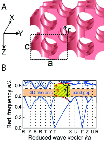
Three-dimensional (3D) nanostructures are drawing a fast-growing attention for their advanced functionalities in nanophotonics Ergin2010Science ; Soukoulis2011NP ; Gansel2009Science ; Wijnhoven1998Science ; Noda2000Science ; Joannopoulos2008book ; Tandaechanurat2011NP , photovoltaics Bermel2007OE ; Upping2011AM and novel 3D integrated circuits and flash memories Crippa2016book ; IBM2012 ; Samsung2014 . The functional properties of such nanostructures are fundamentally determined by their complex internal structure that consist of 3D arrangements of structural units such as spheres, rods, pores, or split-rings Soukoulis2011NP ; Gansel2009Science ; Wijnhoven1998Science ; Noda2000Science . As a representative example, we study here 3D periodic silicon photonic band gap crystals with a cubic diamond-like structure, see Fig. 1A Ho1994SSC ; Maldovan2004NM . These crystals are powerful tools to control the propagation and the emission of light on account of their broad complete 3D photonic band gap Leistikow2011PRL ; Devashish2017PRB , see Fig. 1B. Inevitably, any fabricated nanostructure differs from its initial design, systematically in case of structural deformations Fan1995JAP ; Woldering2009JAP , and statistically in case of size and positional disorder of the structural units Hughes2005PRL ; Koenderink2005PRB . Consequently, the observed functionality differs from the expected one. It is therefore critical to assess the structure of a 3D nanomaterial and verify how well it matches the design.
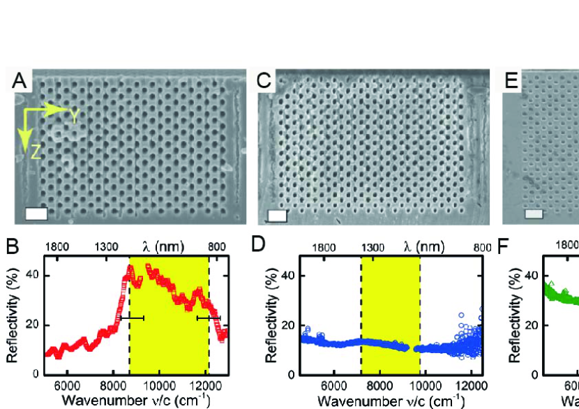
In nanotechnology, a fabricated sample is typically inspected by scanning electron microscopy (SEM) Goldstein2003book . A major limitation of SEM, however, is that only the external surface is viewed whereas the inner structure remains hidden. Indeed, Figure 2 shows three 3D photonic-crystal nanostructures whose external surfaces look closely similar and closely match the design in Fig. 1A. Remarkably, however, the corresponding nanophotonic functionality shown in Figure 2 strongly differs: the crystal shown in panel A reveals a broad photonic gap as designed (panel B), whereas the other two structures reveal no gaps and instead a surprisingly constant reflectivity (panels D,F). To evaluate why a 3D nanostructure is functional or not, it is thus vital to determine the 3D structure non-destructively and in situ with a technique that readily reveals local structural features.
 |
To visualize 3D nanostructures, SEM is supplemented with micro-machining or ion beam milling to cut away part of the structure Goldstein2003book . Unfortunately, however, this approach is destructive, irreversible, and not in situ. While transmission electron microscopy allows for high-resolution 3D imaging, the required sample thickness of less than m is insufficient for monolithic 3D photonic nanostructures Jacobsen1998Book . X-ray techniques are well suited due to their high penetration and high resolution. While small-angle X-ray scattering is employed to study 3D nanoparticle arrays, it naturally operates in reciprocal space, making it hard to characterize local nano-sized features Vos1997Langmuir ; Shabalin2016PRL . In contrast, X-ray tomography yields the real space 3D distribution of the material density Donoghue2006N ; Sakdinawat2010NP . In traditional tomography, the contrast is provided by the sample absorption that is simply related to the brightness of the transmitted image called a radiograph Pollak1953Chest . Since silicon and many materials that prevail in nanotechnology and in complementary metal-–oxide-–semiconductor (CMOS) semiconductor industry absorb X-rays only weakly, however, advanced tomography methods are required.
Here, we obtain the relevant real space structural information directly from the optical phase change of the X-ray beam that propagates through the sample. The phase change is quantitatively retrieved from a set of radiographs taken at multiple sample-to-detector distances while rotating the sample Suppl ; Cloetens1999APL . Following a conventional tomographic reconstruction of the retrieved phase maps, the 3D electron density is obtained in real space as a stack of equally spaced 2D slices in the plane normal to the sample’s rotation axis. To achieve nanometer spatial resolution in a structure with thick (millimeter) substrates that do not need to be cut away, we employ X-ray holographic tomography Mokso2007APL . Its main features are that the X-ray beam is focused and that the sample is placed at a small distance downstream from the focus to collect magnified Fresnel diffraction patterns on the detector.
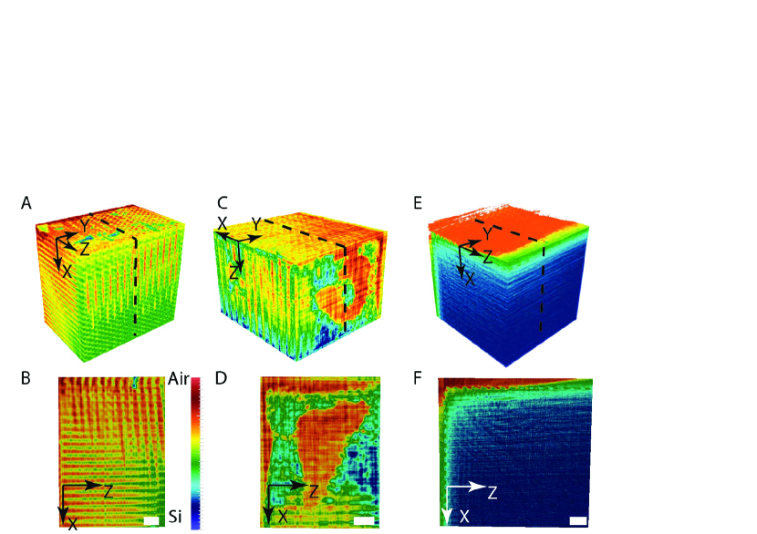 |
Figure 3A shows a bird’s-eye view of the reconstructed sample volume of the 3D photonic crystal shown in Fig. 2A-B. The top face shows the surface of the -directed pores, similar to the SEM surface in Fig. 2A. The alignment of the pores determines the 3D crystal structure and is a crucial step in the nanofabrication. In practice, the alignment is controlled by the etch mask for each pore array and by the directionality of the etching processes vandenBroek2012AFM . In the side face in Fig. 3A, pores are running in the direction, whereas in the front face, pores are running in the direction, matching the 3D design of the inverse woodpile structure (Fig. 1A). In the front face several pores appear as if they are cut and start ”from nowhere” in the middle, which is simply due to their running slightly obliquely to the face, hence the top parts are not seen.
Figure 3B shows an cross-section midway through the 3D reconstructed volume that cuts through both arrays of pores and allows us to determine the maximum depths of both sets of pores. The -pores have a depth nm and a radius nm, corresponding to a state-of-the-art depth-to-diameter aspect ratio , as expected from the deep reactive-ion etching settings vandenBroek2012AFM ; Wu2010JAP . To date, the aspect ratio of pores deeply etched in silicon could only be assessed destructively and ex-situ by SEM inspection of ion-milled slices or cleaved cross sections vandenBroek2012AFM ; Wu2010JAP . The deepest -pores have an even greater depth of nm, corresponding to a high aspect ratio of . Therefore, this is the first unequivocal observation that a second set of deep-etched pores runs even deeper than a first set. Since the pore depth is a main limitation for a crystal’s size, 3D nanostructures are thus significantly larger than expected before. Clearly, Figure 3B already reveals buried structural features that are inaccessible to SEM or other nano-characterization methods (AFM, STM), thus illustrating the power of X-ray holographic tomography.
In addition to characterizing functional nanostructures, X-ray tomography allows to identify several main deviations from design. Figure 3C-D show a bird’s-eye view and a cross-section through a crystal whose external surface revealed usual crystalline features on a SEM image (cf. Fig. 2C). The tomographic reconstruction, however, reveals a buried internal void. The void is caused by well-known stiction (structural collapse) Roman2010JPCM ; Vos2011ECST , as a result of strong capillary forces occurring on the nanoscale during the evaporation of liquid suspension of colloidal quantum dots that was infiltrated to study spontaneous emission Leistikow2011PRL . Thus from tomography we conclude that after these studies, the crystal lost its functionality as a photonic band gap device (see Fig. 2D. Figure 3E-F show a bird’s-eye view and a cross section of another sample whose external surface revealed usual crystalline features on a SEM image (see Fig. 2E). The tomographic reconstruction reveals a structure with pores that appear to be surprisingly shallow (about nm), as a result of inadvertent erroneous settings during the etching process. Thus tomography allows us to conclude that this peculiar structure has no band gap functionality to begin with (see Fig. 2F.
In summary, we performed X-ray holographic tomography of 3D silicon photonic band gap crystals as a generic example of 3D nanomaterials. We obtain the 3D electron density and observe that the structural design is faithfully realized and leads to photonic functionality as expected. In parallel, we uncover several buried structural deviations that help to identify the lack of photonic functionality of faulty structures. We emphasize that the characterization method presented here is non-destructive, since a fabricated sample (up to mm2 cross-section) with buried nanostructures was mounted in the X-ray beam ”as is” (see Methods), without the need for irreversible sample preparation steps. This feature contrasts to recent interesting work where samples had to be destructively milled to a much smaller size Holler2017Nature , or doped with heavy elements to obtain sufficient contrast Chen2012AdvMat . We conclude that X-ray tomography is a powerful tool for structural characterization of any complex 3D functional nanostructure with arbitrary short or long-range order.
References
- (1) T. Ergin, N. Stenger, P. Brenner, J.B. Pendry, M. Wegener, Three-dimensional invisibility cloak at optical wavelengths, Science 328, 337 (2010)
- (2) C.M. Soukoulis, M. Wegener, Past achievements and future challenges in the development of three-dimensional photonic metamaterials, Nature Photon 5, 523 (2011)
- (3) J.K. Gansel et al., Gold helix photonic metamaterial as broadband circular polarizer, Science 325, 1513 (2009)
- (4) J.E.G.J. Wijnhoven, W.L. Vos, Preparation of photonic crystals made of air spheres in titania, Science 281, 802 (1998)
- (5) S. Noda, K. Tomoda, N. Yamamoto, A. Chutinan, Full three-dimensional photonic bandgap crystals at near-infrared wavelengths, Science 289, 604 (2000)
- (6) J.D. Joannopoulos, S.G. Johnson, J.N. Winn, R.D. Meade, Photonic crystals, Molding the flow of light (Princeton University Press, Princeton NJ, 2008) Ed.
- (7) A. Tandaechanurat et al., Lasing oscillation in a three-dimensional photonic crystal nanocavity with a complete bandgap, Nat. Photon. 5, 91 (2011).
- (8) P. Bermel, C. Luo, L. Zeng, L.C. Kimerling, J.D. Joannopoulos, Improving thin-film crystalline silicon solar cell efficiencies with photonic crystals, Opt. Express 15, 16986 (2007).
- (9) J. Üpping et al., Three-Dimensional Photonic Crystal Intermediate reflectors for enhanced Light-Trapping in Tandem solar cells, Adv. Mater. 23, 3896 (2011).
- (10) L. Crippa, R. Micheloni, 3D Charge Trap NAND Flash Memories In: 3D Flash Memories, Ed. R. Micheloni, (Springer, Dordrecht, 2016) pp. 85-127.
- (11) S. Anthony, IBM creates first cheap, commercially viable, electronic-photonic integrated chip, http://www.extremetech.com/computing/142881-ibm-creates-first-cheap-commercially-viable-silicon-nanophotonic-chip (2012).
- (12) Anon., Samsung V-NAND (vertical-NAND) technology (white paper), www.samsung.com/us/business/oem-solutions/pdfs/V-NANDtechnologyWP.pdf (2014).
- (13) K.M. Ho, C.T. Chan, C.M. Soukoulis, R. Biswas, M. Sigalas, Photonic band gaps in three dimensions: new layer-by-layer periodic structures, Solid State Comm. 89 413 (1994)
- (14) M. Maldovan, E. L. Thomas, Diamond-structured photonic crystals Nature Mater. 3, 593 (2004).
- (15) M.D. Leistikow et al., Inhibited spontaneous emission of quantum dots observed in a 3D photonic band gap, Phys. Rev. Lett. 107, 193903 (2011).
- (16) See supplementary material in the Appendix.
- (17) D. Devashish et al., Reflectivity calculated for a three-dimensional silicon photonic band gap crystal with finite support Phys. Rev. B 95, 155141 (2017).
- (18) S.H. Fan, P.R. Villeneuve, J.D. Joannopoulos, Theoretical investigation of fabrication-related disorder on the properties of photonic crystals, J. Appl. Phys. 78, 1415 (1995).
- (19) L.A. Woldering et al., The influence of fabrication deviations on the photonic band gap of three-dimensional inverse woodpile nanostructures, J. Appl. Phys. 105, 093108 (2009).
- (20) S. Hughes, L. Ramunno, J.F. Young, J.E. Sipe, Extrinsic optical scattering loss in photonic crystal waveguides: Role of fabrication disorder and photon group velocity, Phys. Rev. Lett. 94, 033903 (2005)
- (21) A.F. Koenderink, A. Lagendijk, W.L. Vos, Optical extinction due to intrinsic structural variations of photonic crystals, Phys. Rev. B 72, 053102 (2005).
- (22) J. Goldstein et al., Scanning electron microscopy and X-ray microanalysis, (Springer, New York, 2003) 3rd Ed.
- (23) C. Jacobsen, R. Medewaldt, S. Williams, A perspective on biological x-ray and electron microscopy In: X-Ray Microscopy and Spectromicroscopy, Eds. J. Thieme, G. Schmahl, D. Rudolph, E. Umbach, (Springer, New York, 1998) pp. 197-206.
- (24) W.L. Vos, M. Megens, C.M. van Kats, P. Bösecke, X-ray diffraction of photonic colloidal single crystals, Langmuir 13, 6004-–6008 (1997)
- (25) A. G. Shabalin et al., Revealing three-dimensional structure of an individual colloidal crystal grain by coherent X-ray diffractive imaging, Phys. Rev. Lett. 117, 138002 (2016)
- (26) P.C.J. Donoghue et al., Synchrotron X-ray tomographic microscopy of fossil embryos, Nature (London) 442, 680-683 (2006)
- (27) A. Sakdinawat, D. Attwood, Nanoscale X-ray imaging, Nature Photon. 4, 840 (2010)
- (28) B. Pollak, Experiences with planography Dis. Chest. 24, 663 (1953)
- (29) P. Cloetens, W. Ludwig, J. Baruchel, D. van Dyck, J. van Landuyt, J.P. Guigay, M. Schlenker, Holotomography: Quantative phase tomography with micrometer resolution using hard synchrotron radiation x rays, Appl. Phys. Lett. 75, 2912 (1999)
- (30) R. Mokso, P. Cloetens, E. Maire, W. Ludwig, J.-Y. Buffière, Nanoscale zoom tomography with hard x-rays using Kirkpatrick-Baez optics, Appl. Phys. Lett. 90, 144104 (2007)
- (31) J.M. van den Broek et al., Inverse-woodpile photonic band gap crystals with a cubic diamond-like structure made from single-crystalline silicon, Adv. Func. Mater. 22, 25 (2012)
- (32) B. Wu, A. Kumar, S. Pamarthy, High aspect ratio silicon etch: A review, J. Appl. Phys. 108, 051101 (2010).
- (33) B. Roman, J. Bico, Elasto-capillarity: deforming an elastic structure with a liquid droplet, J. Phys. Cond. Mat. 22, 493101 (2010).
- (34) I. Vos, D. Hellin, J. Vertommen, M. Demand, W. Boullart, Silicon nano-pillar test structures for quantitative evaluation of wafer drying induced pattern collapse, ECS Trans. 41, 189 (2011).
- (35) M. Holler, M. Guizar-Sicairos, E.H.R. Tsai, R. Dinapoli, E. Müller, O. Bunk, J. Raabe, G. Aeppli, High-resolution non-destructive three-dimensional imaging of integrated circuits Nature (London) 543, 402 (2017).
-
(36)
Y.C. Chen, J.B. Geddes, L. Yin, P. Wiltzius, P.V. Braun,
X-Ray computed tomography of holographically Fabricated three-dimensional photonic crystals
Adv. Mater. 24, 2863 (2012).
Start of references for Supplementary - (37) D. Gabor, A new microscopic principle, Nature (London) 161, 777 (1948)
- (38) A. Pogany, D. Gao, S.W. Wilkins, Contrast and resolution in imaging with a microfocus x-ray source, Rev. Sci. Instrum. 68, 2774 (1997).
- (39) D. Paganin, Coherent X-ray optics (Oxford University Press, Oxford, 2006).
- (40) J.W. Goodman, Introduction to Fourier optics (Roberts Co, Englewood CO, 2005) Ed.
- (41) G.N. Hounsfield, Computerized transverse axial scanning (tomography): I. Description of system, Br. J. Radiol. 46, 1016 (1973).
- (42) G.T. Herman, Fundamentals of computerized tomography (Springer, London, 2009), Ed.
- (43) J.C. da Silva, A. Pacureanu, Y. Yang, S. Bohic, C. Morawe, R. Barrett, P. Cloetens, Efficient concentration of high-energy x-rays for diffraction-limited imaging resolution, Optica 4, 492-495, 2017.
- (44) A. Mirone, E. Brun, E. Gouillart, P. Tafforeau, J. Kieffer, The pyhst2 hybrid distributed code for high speed tomographic reconstruction with iterative reconstruction and a priori knowledge capabilities, Nucl. Instrum. Meth. B 324, 41-48, 2014.
- (45) A. Guinier, X-ray diffraction: in crystals, imperfect crystals, and amorphous bodies (W.H. Freeman and Co., San Francisco, 1963).
- (46) D.A. Grishina, C.A.M. Harteveld, L.A. Woldering, W.L. Vos, Method to make a single-step etch mask for 3D monolithic nanostructures, Nanotechnology 26, 505302 (2015).
- (47) S. R. Huisman et al., Signature of a three-dimensional photonic band gap observed on silicon inverse woodpile photonic crystals, Phys. Rev. B 83, 205313: 1-7 (2011).
- (48) S.G. Johnson, J.D. Joannopoulos, Block-iterative frequency-domain methods for Maxwell’s equations in a planewave basis, Opt. Express 8, 173 (2001).
- (49) M.R. Teague, Deterministic phase retrieval: a Green’s function solution, J. Opt. Soc. Am. 73, 1434 (1983)
- (50) D. Paganin, S.C. Mayo, T.E. Gureyev, P.R. Miller, S.W. Wilkins, Simultaneous phase and amplitude extraction from a single defocused image of a homogeneous object, J. Microsc. 206, 33 (2002)
I Acknowledgments
This work was supported by the ”Stirring of light!” program of the ”Nederlandse Organisatie voor Wetenschappelijk Onderzoek” (NWO), by the NWO-domain ”Toegepaste en Technische Wetenschappen” (TTW) nr. 11985, the Shell-NWO/FOM programme “Computational Sciences for Energy Research” (CSER), the MESA+ Institute for Nanotechnology (Applied Nanophotonics (ANP)), and by the 2014 Descartes-Huygens Prize of the French Academy of Sciences to W.L.V. We thank ESRF for granting beamtime through experiments HS-2520 and CH-5092.
We thank Leon Woldering, Hannie van den Broek, Willem Tjerkstra, Simon Huisman, Rajesh Nair, Elena Pavlenko, Mehdi Aas, and the MESA+ Nanolab and the ESRF staff for help, and Arie den Boef (ASML), Jean-Michel Gérard (Grenoble), Hans Hilgenkamp, Detlef Lohse, Allard Mosk (Utrecht), Pepijn Pinkse, and Hasan Yilmaz (Yale) for fruitful discussions.
W.L.V. and P.C. conceived the main idea, D.A.G. and C.H. prepared the samples, D.A.G., C.H., A.P., P.C., W.L.V. conducted synchtrotron experiments. D.A.G. and P.C. analyzed the X-ray data, A.P. made the animations. D.A.G., C.H. and W.L.V. conducted optical experiments, D.D. performed theoretical band structure calculations. D.A.G. and W.L.V. wrote the manuscript, with input from all authors. A.L., P.C., and W.L.V. supervised the research. All authors contributed to the analysis and discussion of the results. All data needed to evaluate the conclusions are present in the paper and/or the supplementary materials. Additional data related to this paper may be requested from the authors.
II Supplementary materials
II.1 Materials and methods
II.1.1 3D photonic crystal fabrication
The fabrication process of our 3D photonic band gap crystals is described in detail in Refs. vandenBroek2012AFM ; Grishina2015NT . In brief, a hard mask is defined on a silicon wafer with the centered rectangular array of apertures, with a pore radius that gives the broadest possible band gap Woldering2009JAP . Deep reactive ion etching of the first set of deep pores results in a wafer filled with a large 2D array of deep pores running in the -direction vandenBroek2012AFM . Next, the wafer is cleaved and polished, and the second hard mask is carefully aligned and defined in a area on the side face of the wafer. By etching the second set of pores in the -direction, the 3D structure is obtained in the volume where both sets of pores overlap, see Figure 3 and the movie animations M1-M2. Finally, the hard mask is removed. 3D photonic crystals shown in Figure 3A-D are fabricated in the above mentioned way and are buried on chips with cross-section up to mm2.
In our second generation of photonic crystals, the etch mask is deposited in a single step on both faces of a wafer edge Grishina2015NT , followed by deep reactive ion etching of two perpendicular arrays of pores. The 3D photonic crystal shown in Figure 3E-F is an example of a second generation photonic crystal fabricated with the single-step etch mask. While this particular sample turned out to be not successful, this fabrication route has yielded many other samples that had the intended 3D structure, as confirmed by X-ray tomography.
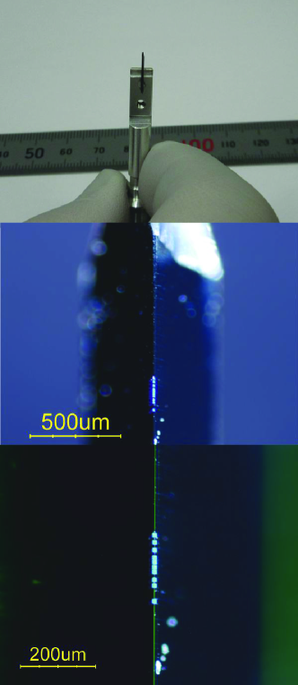
Figure S1. Photographs of a typical sample studied by X-ray tomography. Top: A silicon beam with photonic crystal structures is mounted in a holder for the X-ray tomography scans. Center: Zoom-in of the top part of the Si beam, with a vertical row of 3D photonic crystal structures on the edge of the beam. In the defocused background, the edges of the beam’s inclined surfaces are visible. Bottom: Further zoom-in reveals ten 3D photonic crystal structures that display a blueish iridescence due to their periodic surface structure. The edge of the beam appears as the vertical green line of scattered light.
Figure 4 (S1) shows photographs of a sample as it is studied in the X-ray tomography instrument. The silicon beam measures mm3 and is shown after preparation in the MESA+ Nanolab, and mounted for X-ray tomography scans in the ESRF. We emphasize that there is no need to cut a specific area out of the sample using focused-ion beam (FIB) milling, as opposed to other imaging techniques that require small sample volumes, such as X-ray ptychography, transmission electron microscopy (TEM), FIB-SEM, and so forth. We have successfully mounted several samples characterized by X-ray holographic tomography at ESRF in optical setups in Twente without further modifications, and even in the same sample holder.
A feature in Figure 3B is that the pores running in the -direction are not exactly perpendicular to the pores in the -direction. It appears that the angle between the pore arrays deviates from the design by ; from results on several crystals we find deviations between and . We attribute the slight variations to the limited precision in placing a sample in the etching chamber. From separate plane-wave band structure calculations we find that the 3D photonic band gap is robust to the slight shear of the cubic crystal structure Woldering2009JAP .
II.1.2 Synchrotron X-ray holographic tomography
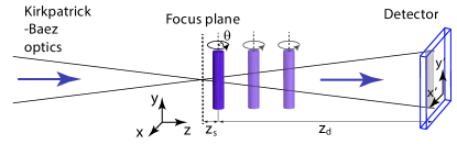
Holographic tomography experiments were performed at the European Synchrotron Radiation Facility (ESRF), on the nano-imaging beamline ID16A-NI Dasilva2017Optica . The X-ray beam with keV photon energy propagates in the -direction and is focused with multilayer coated Kirkpatrick-Baez optics to a nm2 focus. The sample is placed at a small distance downstream from the focus, while the detector is placed at the distance downstream from the sample, see Figure 5. The image recorded in the detector plane is an in-line Gabor hologram or Fresnel diffraction pattern Gabor1948Nature . Due to the focusing, the sample is illuminated with a spherical wave, unlike the plane-wave illumination in traditional tomography. According to the Fresnel scaling theorem, the spherical wave illumination gives rise to an effective propagation distance and a magnification given by Pogany1997RSI ; Paganin2006book
| (1) |
Varying the focus-to-sample distance allows us to vary the magnification of the diffraction patterns. It also strongly modifies the Fresnel diffraction pattern recorded on the detector through the effective propagation distance. For a phase periodic object such as our photonic band gap crystals, the Talbot effect results in zero contrast for certain spatial frequencies at the characteristic Talbot distances Goodman2005Book . To obtain non-zero contrast at all spatial frequencies, data are taken at four distances . The first distance was chosen to obtain a desired pixel size, either 10 or 20 nm. At each distance , images were recorded with s exposure time while rotating the sample from to around the -axis of the crystal (see Fig. 2) . For the tomographic scans, the axis of rotation was aligned to be a few deep inside the silicon.
The data processing is a two-step procedure consisting of a phase retrieval step followed by a tomographic reconstruction. The phase retrieval aims at retrieving the amplitude and phase of the wave exiting the sample and that are given by
| (2) |
and
| (3) |
with the X-ray wavelength. The amplitude and phase are thus the projection of respectively the absorption index and the refractive index decrement that determine the complex refractive index for hard X-rays
| (4) |
Prior to phase retrieval, all sets of radiographs are scaled to the same magnification and mutually aligned. We determine a first estimate of the amplitude and phase using the approach proposed by Paganin et al. Paganin2002JM , and extended to multiple distances. Here, we assume a homogenous ratio for silicon at an X-ray energy of keV. This first estimate provides only a blurred version of the phase map. The map is recursively improved using iterations of a non-linear least squares optimization. The phase retrieval was carried out with ESRF in-house software using the GNU Octave programming environment (www.octave.org) and the public domain image analysis program ImageJ (see http://rsbweb.nih.gov/ij).
Secondly, a standard tomographic reconstruction Hounsfield1973BJR based on the filtered back-projection algorithm Herman2009Book and implemented in the ESRF software PyHST2 Mirone2014NIMB allows us to obtain the distribution of the refractive index decrement . Since the X-ray energy of keV is far above any absorption edge of the materials under investigation, we obtain the electron density distribution from the well-known expression Guinier1963Book
| (5) |
with the classical electron radius. The resulting structure was rendered with open-source software ParaView (see www.paraview.org).
II.1.3 Nanophotonic experiments
To assess the basic functionality of the photonic crystals, we performed optical reflectivity to probe the designed photonic gaps. Optical reflectivity was measured using a home-built microscope setup that employs reflective optics and operates in the near infrared range (at wavelengths beyond nm, see Ref. Huisman2011PRB . Main components are a supercontinuum white light source (Fianium), a Fourier-transform interferometer (Biorad FTS-6000) that operates with cm-1 spectral resolution, and a reflecting objective to focus the beam to a few microns inside the photonic crystal domains over the large required range of frequencies. Signals were collected in the near infrared spectral range between about cm-1 and more than cm-1 (corresponding to wavelengths between and nm). Reflectivity was calibrated by taking the ratio of a sample spectrum with the spectrum measured on a clean gold mirror. In the spectra in Figs. 2B,D,F a narrow range near cm-1 is omitted since it is disturbed by the pump laser of the supercontinuum source. The maximum reflectivity in Fig. 2B is limited to due to several different reasons: the white light focus has a diameter (m) comparable to the extent over which the crystal is homogeneous; near the crystal-air interface the pores reveal roughness as a result of the etching process (so-called ”scallops” Wu2010JAP ; vandenBroek2012AFM ).
II.1.4 Photonic band structure calculations
Photonic band structures were calculated with the plane-wave expansion method, using the MIT photonic bands (MPB) code Johnson2001OE . Silicon was modeled with a dielectric function , and the unit cell was discretized with a high spatial resolution . The band structures are represented as reduced frequency versus reduced wave vector between high-symmetry points (R, Y, S, R, T, Y, , X, U, , Z, U, R) in the 1st Brillouin zone of the convenient tetragonal representation of the unit cell Joannopoulos2008book . The polarization states of the photonic bands that bound the stop gap (or symmetrically equivalently the gap) (see Figure 1B) were assigned based on our recent computational study Devashish2017PRB . The photonic bands in Figure 1B and the gap in Figure 2B were calculated for a relative pore radius as borne out of the X-ray tomography data, and the gaps in Figures 2D,F were calculated for the designed pore radius .
II.2 Multimedia files
In view of the richness of the 3D reconstructions, we provide three movie animations of rotations about and cross-sections through the 3D data volumes, in AVI format.
-
1.
Animation ’theGood1.avi’: Color animation of a rotation of the successfully etched crystal shown in Fig. 3A-B about the vertical axis in Fig.3 A. The animation shows the reconstructed sample volume from all viewing directions. Still at :
-
2.
Animation ’theGood2.avi’: Black and white animation of YZ cross-sections scanned in the X-direction through the volume of the successfully etched crystal shown in Fig. 3A-B. The scan starts from the bottom in the substrate, scans parallel to X-oriented pores to show Z-oriented pores, and finishes in air above the crystal. Still at :
-
3.
Animation ’theBad.avi’: Black and white animation of YZ cross-sections scanned in the X-direction through the volume of the crystal with a void shown in Fig. 3C-D. The scan starts from the bottom in the substrate, scans parallel to X-oriented pores while traversing the stiction-induced void (where the surrounding 2D photonic crystal pores are still apparent left and right), and finishes in air above the crystal surface. Still at :
Since the unetched (”the Ugly”) sample (Fig. 3E-F) reveals mostly cross-sections through bulk silicon, we have decided against an animation for this sample.