[table]capposition=top
Optimization approach for optical absorption in three-dimensional structures including solar cells
Benjamin J. Civilettia,
Tom H. Andersona,
Faiz Ahmadb,
Peter B. Monka, and
Akhlesh Lakhtakiab
aUniversity of Delaware, Department of Mathematical Sciences,
501 Ewing Hall, Newark, DE 19716, USA
bPennsylvania State University, Department of Engineering Science and Mechanics, NanoMM–Nanoengineered Metamaterials Group, University Park, PA 16802, USA
Abstract
The rigorous coupled-wave approach (RCWA) and the differential evolution algorithm (DEA) were coupled in a practicable approach to maximize absorption in optical structures with three-dimensional morphology. As a model problem, optimal values of four geometric parameters and the bandgaps of three -layers were found for an amorphous-silicon, multi-terminal, thin-film tandem solar cell comprising three -- junctions with a metallic hexagonally corrugated back-reflector. When the optical short-circuit current density was chosen as the figure of merit to be maximized, only the bandgap of the topmost -layer was significant and the remaining six parameters played minor roles. While this configuration would absorb light very well, it would have poor electrical performance. This is because the optimization problem allows for the thicknesses and bandgaps of the semiconductor layers to change. We therefore devised another figure of merit that takes into account bandgap changes by estimating the open-circuit voltage. The resulting configuration was found to be optimal with respect to all seven variable parameters. The RCWA+DEA optimization approach is applicable to other types of photovoltaic solar cells as well as optical absorbers, with the choice of the figure of merit being vital to a successful outcome.
1 INTRODUCTION
Three items are needed to numerically optimize the design of an optical absorber such as a thin-film solar cell. The first item is a fast solver that can predict the performance of the device in a variety of configurations. The second item is an optimization code that can mitigate the effect of local minima without excessive computational time. The third item is a figure of merit that adequately captures the desired performance characteristics of the device so that a good design will emerge. Some of these choices are explored in this paper.
The rigorous coupled-wave approach (RCWA) [1, 2] can be used to model the optical performance of a thin-film optical absorbers, as has been shown for solar cells with metallic back-reflectors that are periodically corrugated along one direction [3, 4, 5]. Indeed, the RCWA provides accurate results with high computational speed for boundary-value problems involving structures that are invariant only along, say, the axis and therefore are quasi-two-dimensional [6, 7]. Furthermore, the RCWA can be coupled with the differential evolution algorithm (DEA) [8, 9] for optimization [5]. However, the computational requirements of RCWA increase significantly when the back-reflector is periodically corrugated in two directions, i.e., the boundary-value problem is fully three-dimensional (3D) in nature [10, 11]. Additional design parameters enter the optimization process thereby to increase the computational burden further.
The dimensions of the unit cell of an optical absorber with a PCBR directly affect optical absorption [5]. Optimization of thin-film solar cells with two-dimensionally corrugated back-reflectors for maximum absorption has not been reported heretofore, to our knowledge. As a preliminary study showed that it is becoming a practicable proposition with commonly available computational resources, we decided to implement the RCWA+DEA approach to optimize a fully 3D absorbing structure [12].
To demonstrate this approach, we report here the maximization of optical absorption in an idealized thin-film tandem solar cell fabricated over a periodically corrugated back-reflector (PCBR) with hillock-shaped corrugations arranged on a hexagonal lattice. The active region of the chosen solar cell comprises three electrically isolated -- junctions. The semiconductor layers were taken to have the bandgap-dependent optical properties of amorphous silicon.[13] Silver [14] is a good choice for the PCBR because its plasmonic nature can be harnessed to launch surface-plasmon-polariton (SPP) waves inside the device and thereby enhance the optical electric field and optical absorption [15, 16, 17]. With the foregoing choices, our results indicate that maximization of the optical short-circuit current density, the standard figure of merit,[18, 19, 20] does not result in a desirable design. Instead, we found that the maximum power density is a better figure of merit.
The plan of this paper is as follows. The optical boundary-value problem that is solved to determine the spectrally integrated number of absorbed photons per unit volume per unit time is presented in Sec. 2. The numerical techniques adopted for this work are presented in Sec. 3: the three-dimensional implementation of the RCWA is briefly described in Sec. 3.1, Sec. 3.2 contains the diagonalization of a matrix that emerges in the RCWA implementation, and Sec. 3.3 briefly describes the DEA. Numerical results are provided in Sec. 4, Sec. 4.3 discusses the convergence of the numerical methods, while Sec. 4.4 briefly compares these numerical results to a thin-film tandem solar cell with a bi-sinusoidal PCBR. Closing remarks are presented in Sec. 5.
The free-space wavenumber, angular frequency, and intrinsic impedance of free space are denoted by , , and , respectively, where is the free-space wave length, is the permeability of free space, is the permittivity of free space, and is the speed of light in free space. Vectors are underlined, column vectors and matrices associated with the RCWA are in boldface with breve notation, and the Cartesian unit vectors are identified as , , and . The imaginary unit is denoted by .
2 MODEL BOUNDARY-VALUE PROBLEM
We considered the boundary-value problem shown schematically in Fig. 1, which also defines the thicknesses , and . The device occupies the region
| (1) |
with the half spaces and occupied by air. The reference unit cell is identified as , the back-reflector (which also functions as an electrode in a solar cell) being doubly periodic with period along the axis and period along the axis.
The region comprises an antireflection window and three -- junctions which are electrically isolated from each other by two windows, as shown in Fig. 1(a). The relative permittivity of this multilayered material depends on . The layers are identified in the figure. All windows are made of a material of relative permittivity . The -dependent relative permittivity of each semiconductor layer depends on the bandgap chosen for that layer.
The region is occupied by a metal with relative permittivity . The region , henceforth termed the grating region, contains a periodically undulating surface with period along the axis and period along the axis. The unit cell in the plane was chosen to form a two-dimensional rectangular lattice that is equivalent to a hexagonal lattice. If the side of the regular hexagons in this lattice is denoted by , then and for the rectangular lattice.
[figure]style=plain,subcapbesideposition=top,font=bf
\sidesubfloat[]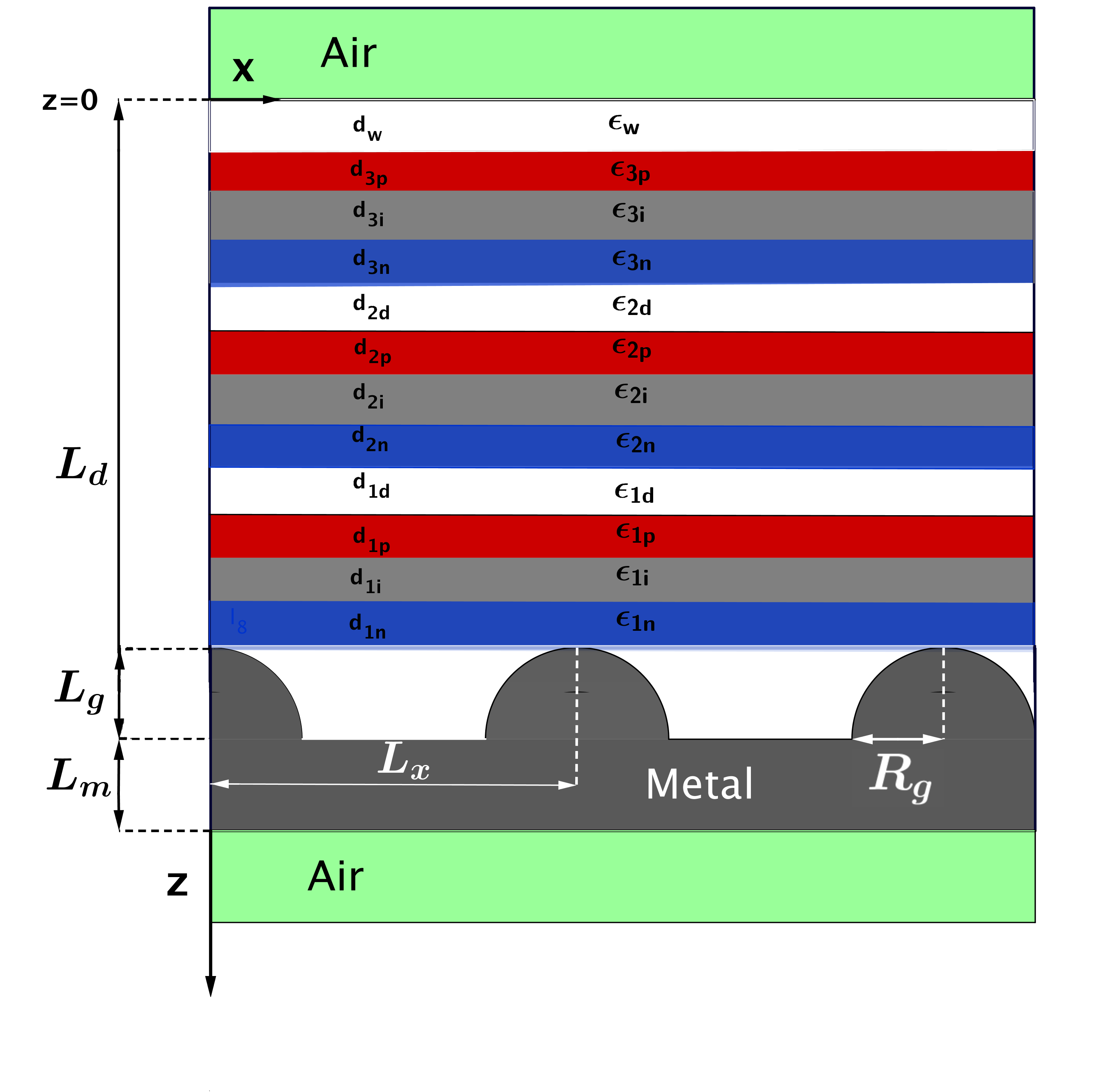 \sidesubfloat[]
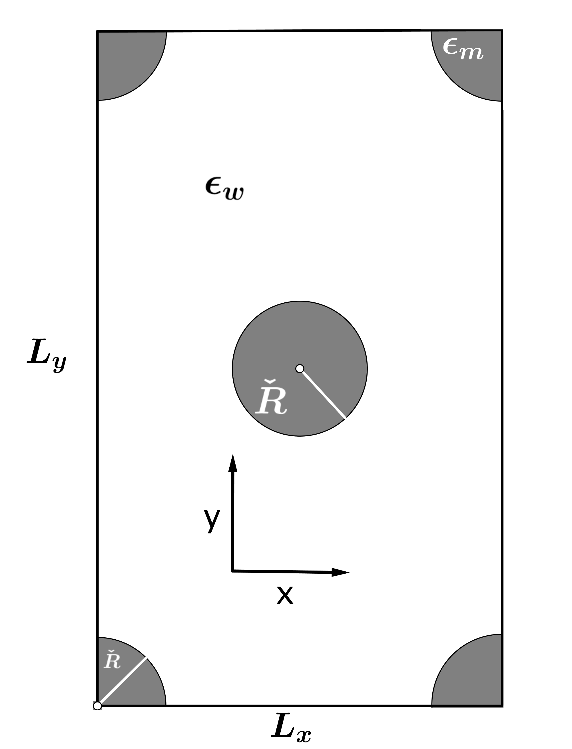
|
The grating region is defined by hillocks arranged as in Fig. 1(b). Each hillock is a frustum of a sphere of radius . The base of the hillock is a circle of radius and the height of the hillock equals , as shown in Fig. 1(a); accordingly,
| (2) |
The intersection of the plane and a hillock is a circle of radius
| (3) |
The relative permittivity in the grating region is
| (4) |
with
| (5) |
where is the minimum distance between the point and the centers , , , and of the circle and four quarter circles in Fig. 1(b).
3 Numerical Techniques Used
3.1 Rigorous coupled-wave approach
The RCWA was used the calculate the electric field phasor everywhere inside the chosen device as a result of illumination by a monochromatic plane wave normally incident on the plane from the half space . The electric field phasor of the incident plane wave was taken as
| (6) |
where V m-1.
As a result of the PCBR being doubly periodic, the - and -dependences of the electric and magnetic field phasors have to be represented everywhere by Fourier series as
| (7) | ||||
| and | ||||
| (8) | ||||
where , , and as well as are Fourier coefficients. Likewise, the relative permittivity everywhere is represented by the Fourier series
| (9) |
where are Fourier coefficients. Substitution of Eqs. (7)–(9) in the frequency-domain Maxwell curl postulates yields the matrix ordinary differential equation [21, Chap. 3]
| (10) |
where the column vector contains the - and -directed components of the Fourier coefficients of the electric and magnetic field phasors.
Detailed descriptions of the algorithm to solve Eq. (10) are available elsewhere [12, 21]. In brief, computational tractability requires the foregoing expansions to be truncated to include only and , with and . The region is partitioned into a sufficiently large number of slices along the axis. Each slice is taken to be homogeneous along the axis but may be periodically nonhomogeneous along the and axes. Thus, the matrix is assumed to be piecewise uniform in . Boundary conditions are enforced on the planes and to match the fields to the incident, reflected, and transmitted fields, as appropriate. A stable marching algorithm is then used to determine the Fourier coefficients of the electric and magnetic field phasors in each slice[21]. Finally, the -directed components of the electric and magnetic field phasors in the device can be obtained through algebraic equations arising during the derivation of Eq. (10). Thus, the electric field phasor can be determined throughout the solar cell.
The spectrally integrated number of absorbed photons per unit volume per unit time is given by
| (11) |
where is the reduced Planck constant, is the AM1.5G solar spectrum [22], nm, and nm. With the assumption that the absorption of every photon in a semiconductor layer releases an electron-hole pair, the charge-carrier-generation rate equals , which can be determined at any location in the nine semiconductor layers. The integral on the right side of Eq. (11) was approximated using the trapezoidal rule [23] with the integrand uniformly sampled every nm.
3.2 Diagonalization of
The numerically stable RCWA algorithm requires that be diagonalizable [24] in each slice for every [21, Sec. 3.8]. As the relative permittivity is not uniform in any slice in the grating region, the built-in function eig in Matlab® (version R2016b) was used to compute the eigenvalues and eignenvectors of . In all other slices, the eigenvalues and eigenvectors of were determined analytically, to increase the computational speed.
A superindex
| (12) |
is defined for convenience, where .[21] In any slice in which the relative permittivity is independent of and , the distinct eigenvalues of are given by
| (13) |
with each eigenvalue having an geometric multiplicity of , , and . Half of the eigenvectors are
| (14) | |||||
In the column vector on the right side of Eq. (14), the non-zero entries occur in the following locations (counting from the top): , , and . The remaining eigenvectors are
| (15) | |||||
The non-zero entries occur in the column vector on the right side of Eq. (15) in the following locations (counting from the top): , , and .
3.3 Differential evolution algorithm
We employed the DEA to maximize a figure of merit over a variety of optical and electrical parameters numbering . The DEA has been used previously[5] for seeking optimal designs of PCBRs that are invariant along the axis, as the algorithm is well-suited to search a large space of candidate solutions. The number of candidate solutions depends on the number of parameters and discretization of parameter ranges for the optimization.
To maximize the figure of merit , we wish to find an optimal point , where is a search space of all possible parameter combinations.
We note that the DEA requires that all parameter ranges be discretized, so the search is conducted over a finite number of possible outcomes. The DEA requires specification of the crossover probability , a differential weight and the number of random points . Details of the algorithm have been provided elsewhere[5, 8, 9].
The DEA is very useful for solving complicated optimization problems, but it does not guarantee convergence to a global extremum [25]. However, stochastic sampling of the search space helps to avoid local maxima.
4 NUMERICAL RESULTS AND DISCUSSION
In this paper we have chosen to maximize optical absorption. The figures of merit defined later in this section take into account all optical effects such as the excitation of SPP waves and waveguide modes [26]. This allows a tradeoff between the various optical phenomena without prejudicing one mechanism over another. However, the parameter space is chosen so that the excitation of SPP waves and waveguide modes can be supported.
For all numerical results in this paper, the window layers were chosen to be made of alumimum-doped zinc oxide (AZO). For the two windows between -- junctions, the thicknesses were fixed so that nm. The relative permittivity of AZO was taken from a standard source[27]. The minimum thickness of the PCBR was fixed at nm. The metal was chosen to be silver, whose relative permittivity also depends on [14].
The bandgaps , , of the -layers in the triple-junction solar cell were kept variable in the range eV, but their thicknesses nm were kept fixed. The thicknesses of all three -layers and all three -layers were also kept fixed: nm. The bandgaps of all three -layers were fixed as eV, . The bandgaps of the -layers were fixed as follows: eV and eV.
By introducing C or Ge into the lattice, a new material is formed, but the -layers are still of the a-Si:H_GeC family. This process changes the bandgap, where the -dependent relative permittivity of the material is obtained by an analytical model.[17, 13]. The electrical properties of the material also change, and can be found by applying Vegard’s law to known values.[28] Since the electrical properties have no effect on our optical model, they have no role in this study.
Furthermore, the lattice parameter nm, the antireflection window’s thickness nm, the base radius nm, and the corrugation height nm were allowed to vary. Thus, the dimension of the search space was , and we sought an optimal design over a candidate space of possible configurations. We used parameter values , , and for optimization.
4.1 Optimization for optical short-circuit current density
The figure of merit for the DEA optimization was initially chosen to be standard figure of merit for optical modeling of solar cells[29]: the optical short-circuit current density
| (16) |
where is the portion of the reference unit cell occupied by the nine semiconductor layers in the solar cell. and C is the elementary charge. This figure of merit will maximize the number of photons absorbed in the solar cell, but disregards all electrical properties. In this section we proceed to show that this results in a poor design.
 |
 |
| (a) | (b) |
 |
|
| (c) |
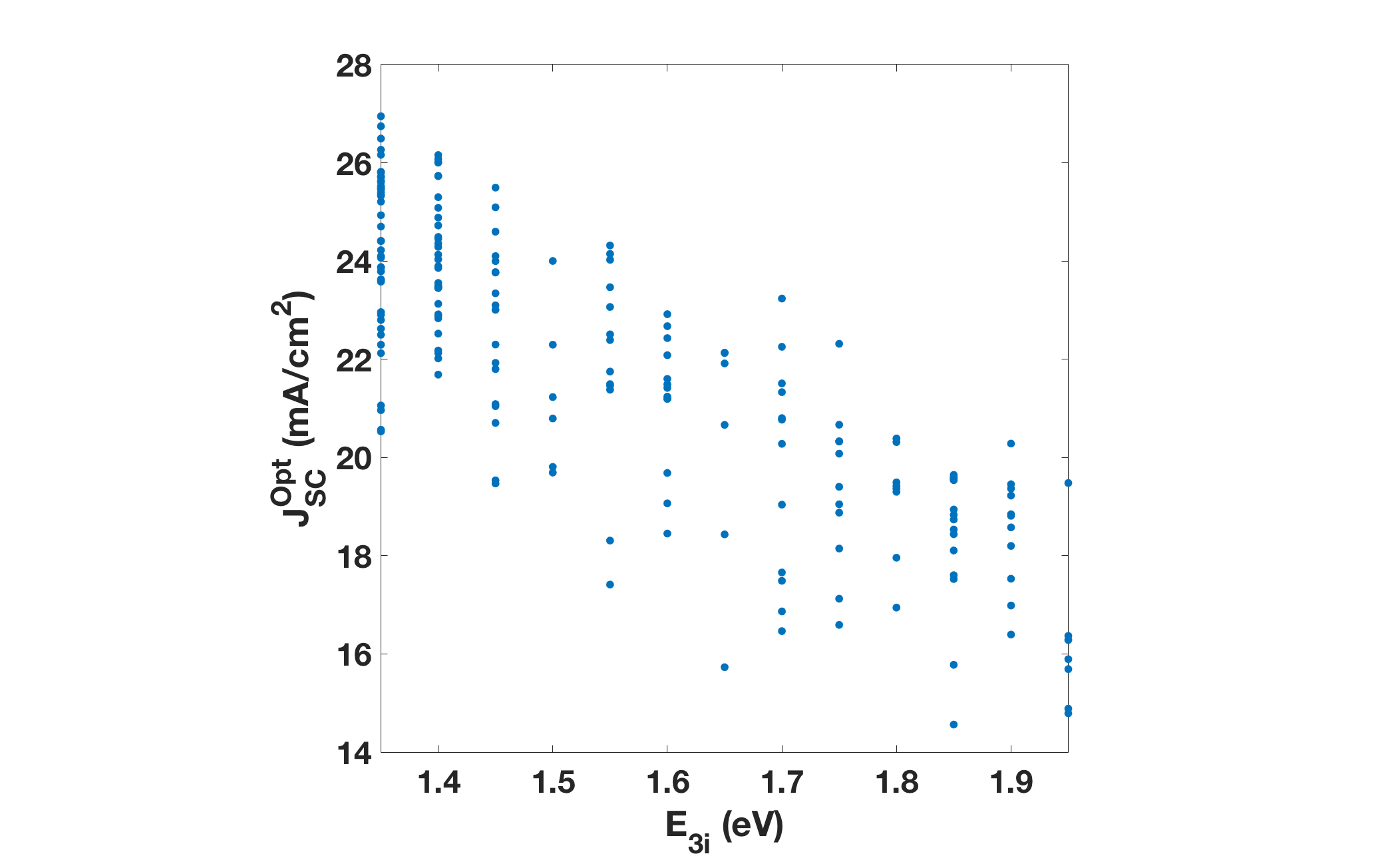
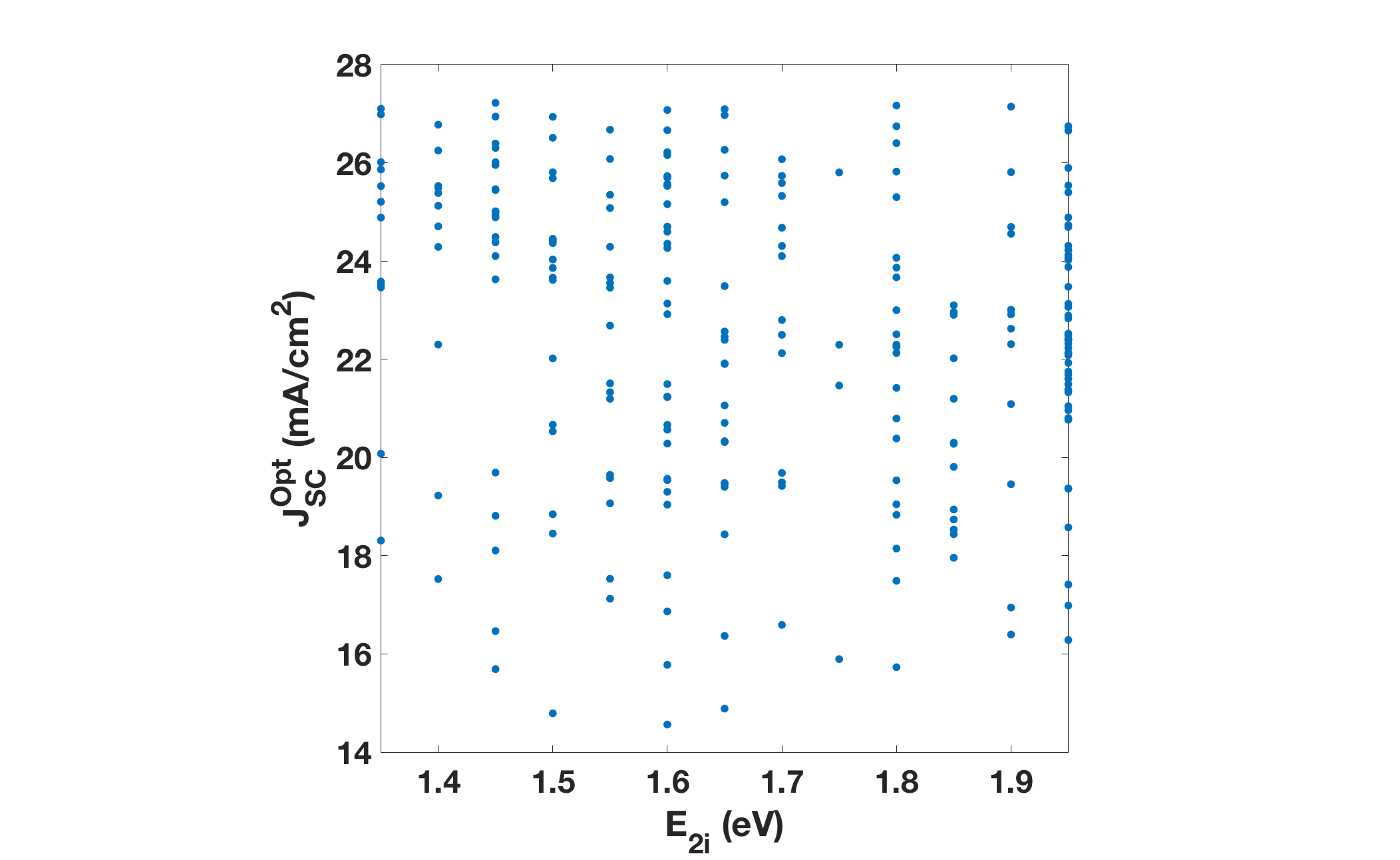
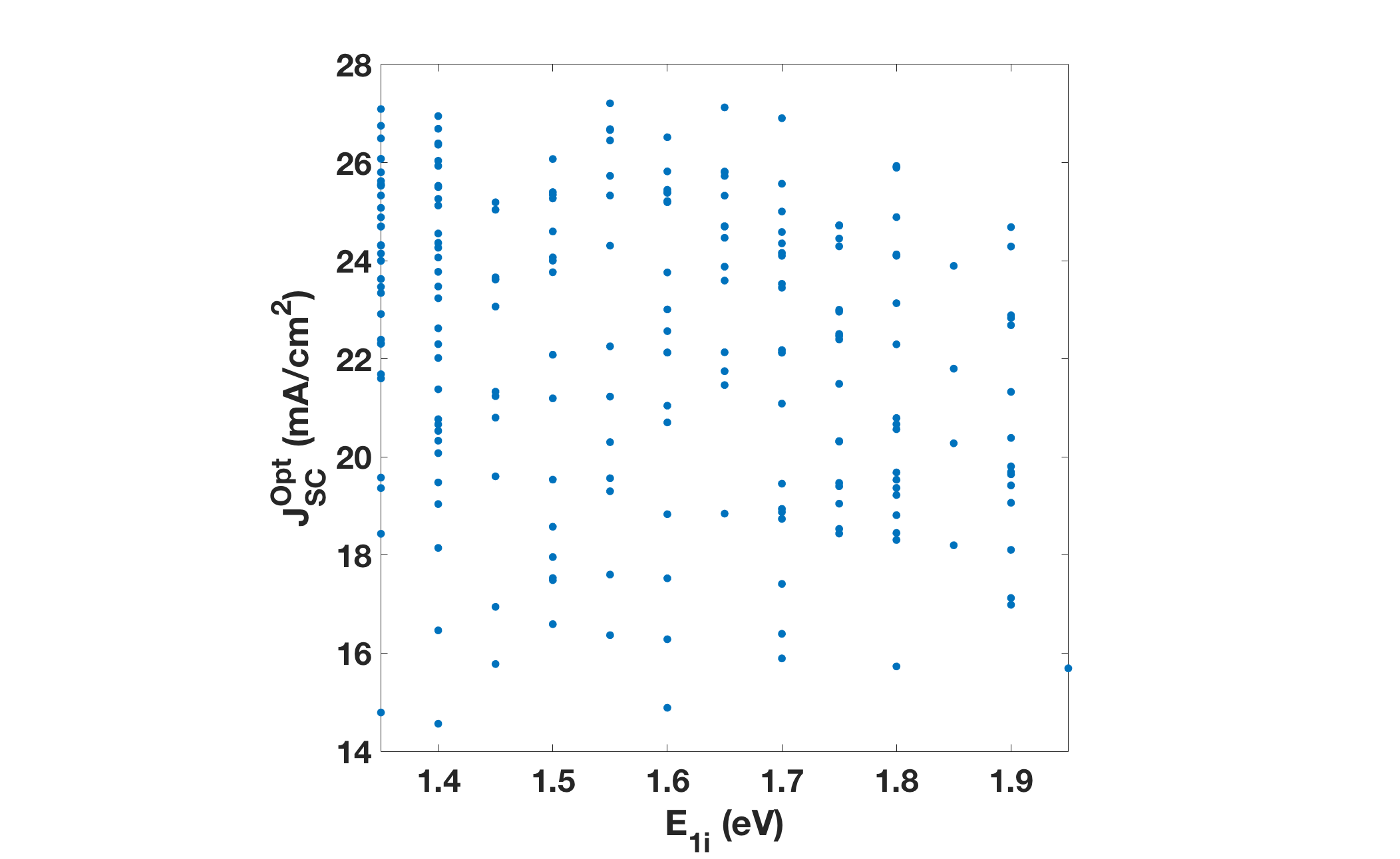
Plots of against the bandgaps , , for points sampled by the optimization exercise are presented in Fig. 2. In this figure as well as in Fig. 3, the data points from DEA are projected onto the plane formed by the variable being investigated and the figure of merit. The bandgap of the topmost –layer is the most influential parameter that controls . While attempting to maximize , the DEA minimized the bandgap in this layer, and we see that many parameter sets with eV at the boundary of the constraint set were evaluated. As increases from eV to eV, decreases throughout most of this interval as shown in Fig. 2(a).
Maximization of showed that minimizing was the most important factor compared with the remaining variable parameters (i.e., , , , , , and ). This phenomenon is clearly exemplified in Fig. 2(a), where for any fixed value of , the remaining variable parameters contribute only to a mA cm-2 variation in . Unfortunately, such a configuration is likely to be electrically inefficient: with a narrow bandgap, more charge carriers are excited, but the operating voltage of the solar cell will be reduced. [30] Contrast this to Figs. 2(b) and (c) wherein the variations of with the bandgaps and , respectively, are shown. We see that while is maximum when eV, there are values of ranging from mA cm-2 to mA cm-2.
Parenthetically, when the thicknesses of the -layers were included as variables in an optimization exercise, the DEA simply focused on the maximization of those thicknesses. The resulting configuration would also have poor electrical performance. While this type of solar cell would absorb more light, an excited charge carrier would have to travel further to reach an electrode, thereby increasing recombination and decreasing efficiency. We note that Fig. 2 demonstrates the choice of figure of merit is very important. We only included these results to contrast them with numerical results in Fig. 5, since all the chosen parameters in the optimization exercise should affect the solar-cell performance.
4.2 Optimization for maximum power density
In order to improve the optimal design of the chosen solar cell without including a full electrical model, we devised a new figure of merit for the DEA which penalizes the effect of minimizing the bandgap of any of the -layers. We defined the power density
| (17) |
as the new figure of merit, with being the region occupied by the -th -- junction. Let us note that is a theoretical upper bound on the maximum extractable power density of the solar cell. Furthermore, the summation over the index indicates that the tandem solar cell is to be configured in the multi-terminal format. Note that this power density is computed solely from the absorption of photons and the material bandgap. This estimates the maximum electrical power density but does not involve any electrical modeling (e.g., recombination and mobility of electrons and holes). A useful extension of our approach would be to include an electrical model, but that extension lies beyond the scope of this paper.
 |
 |
| (a) | (b) |
 |
 |
| (c) | (d) |
 |
 |
| (a) | (b) |
 |
 |
| (c) | (d) |
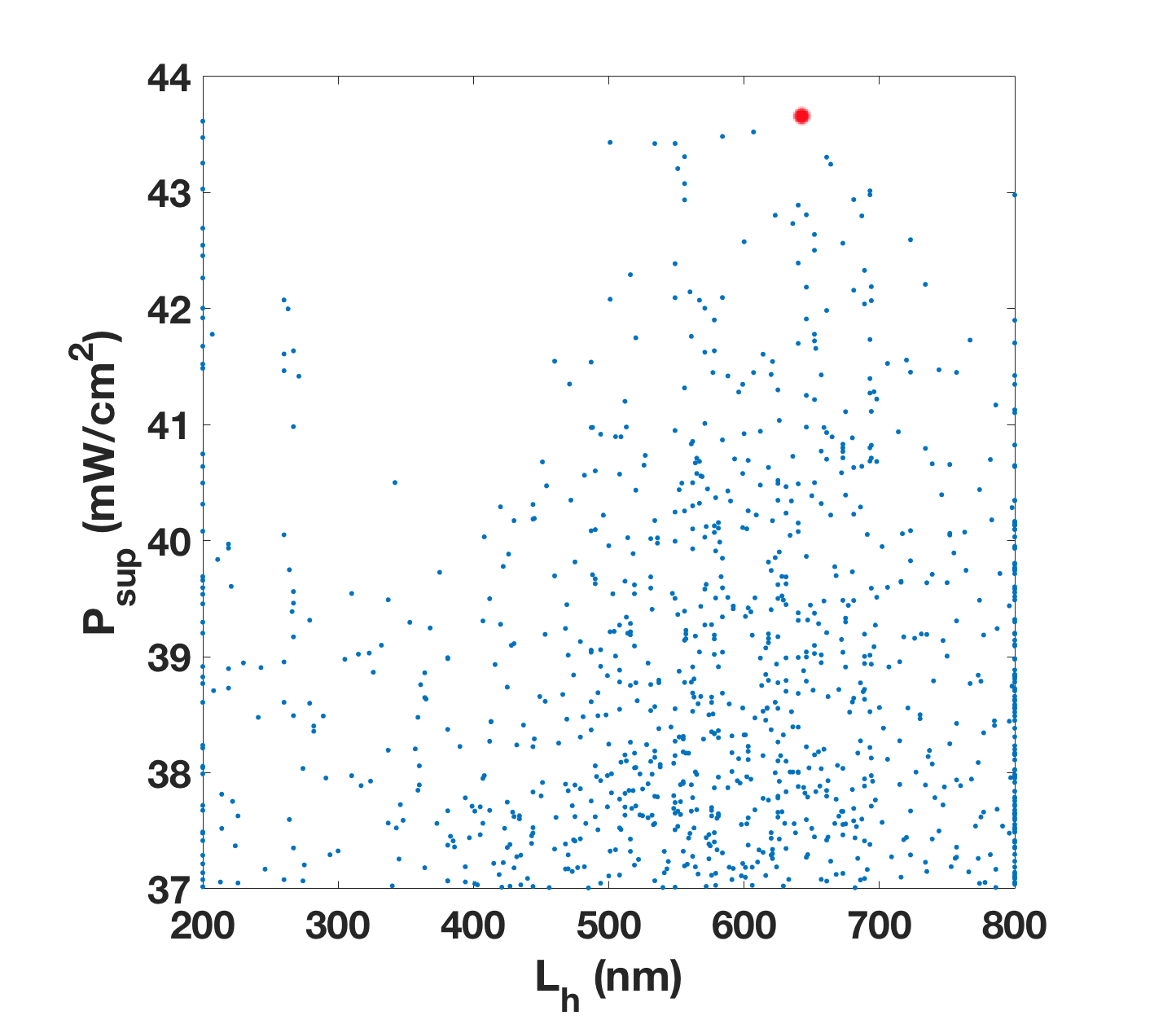
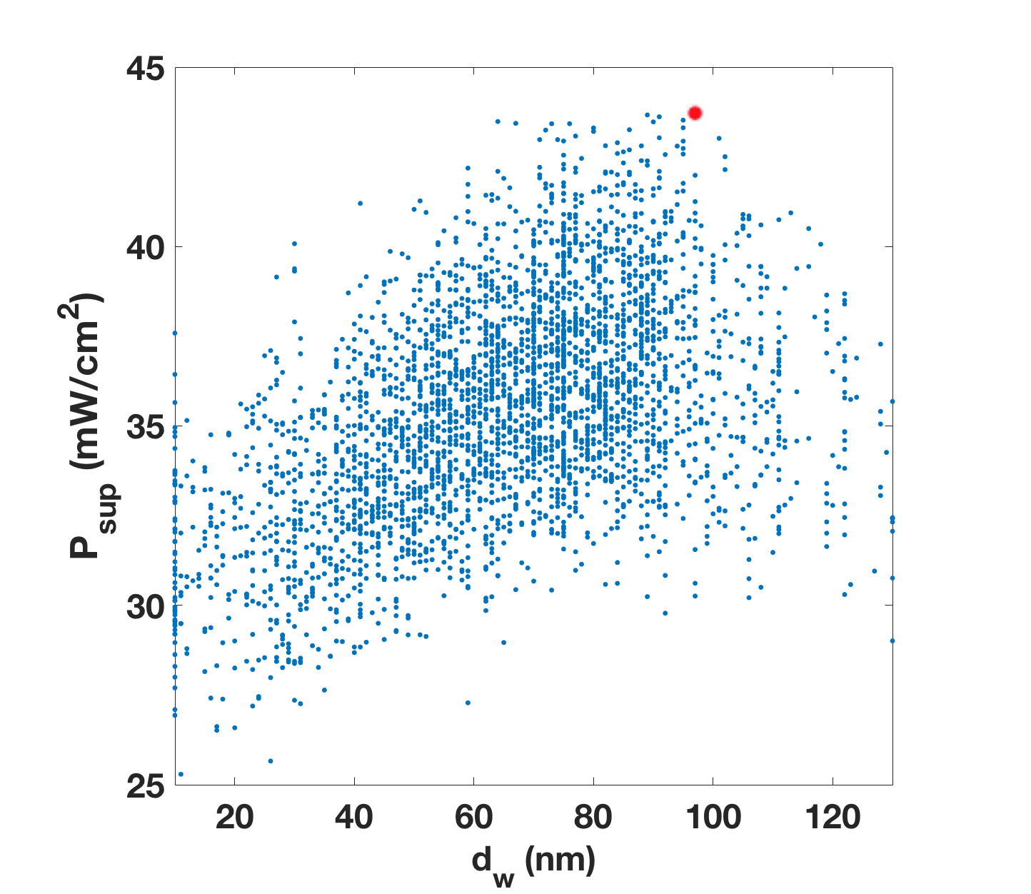
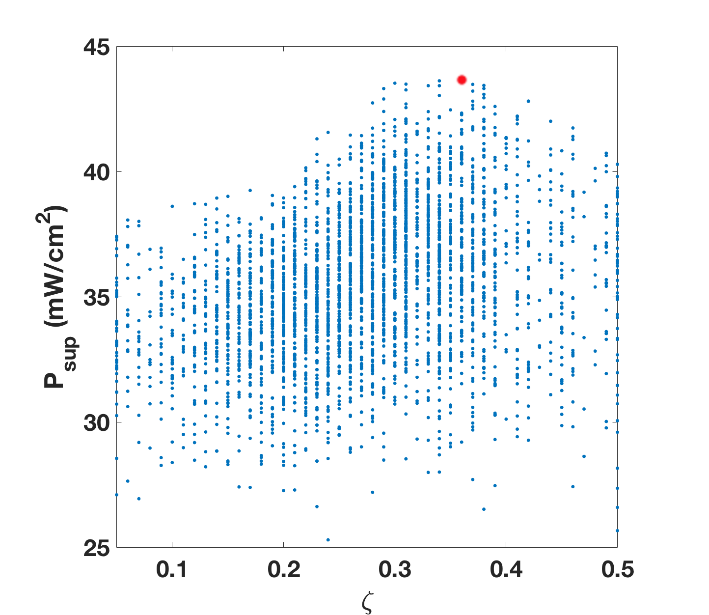
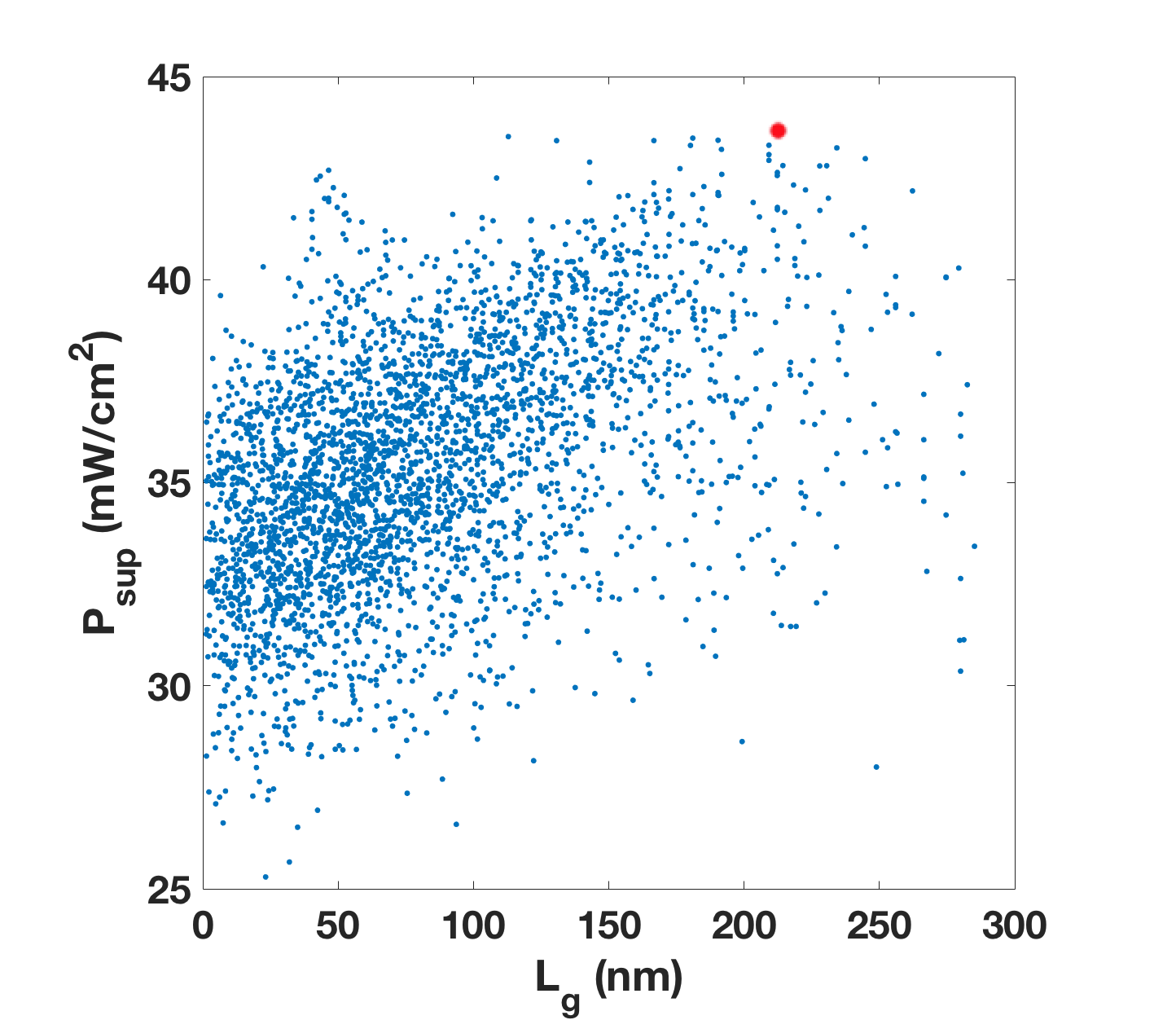
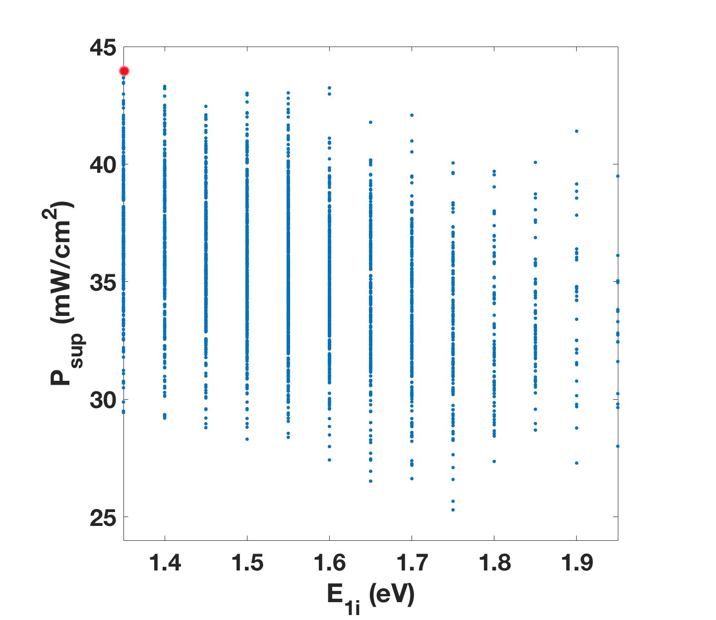
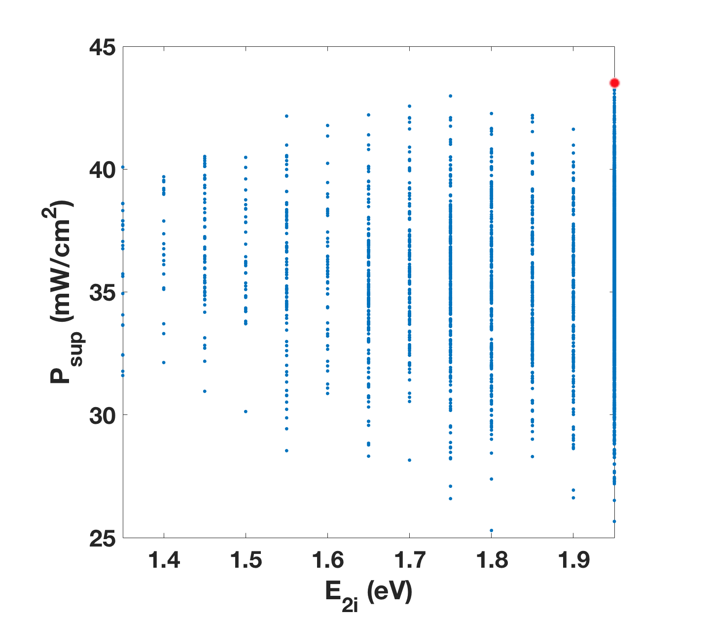
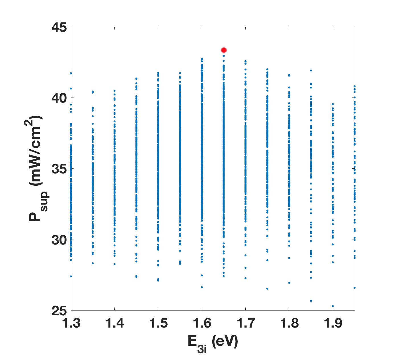
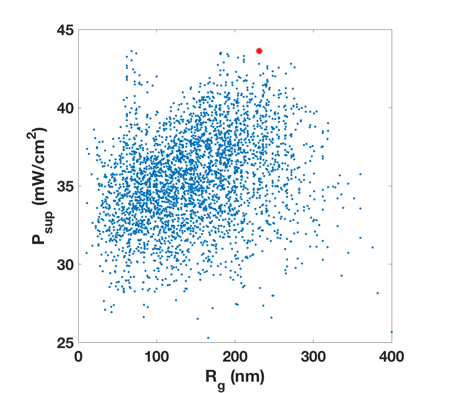
Figures 3 and 4 show the results of the DEA optimization for the variable geometric and bandgap parameters of the solar cell—namely, the lattice parameter , the antireflection-window thickness , the duty cycle , the corrugation height , and the bandgaps , , and . All seven of these parameters influence the figure of merit defined by Eq. (17). Indeed, a steady increase in is seen in Fig. 3(a) on the interval nm; a very sharp increase in is evident in Fig. 3(b) as increases from nm to nm; increases steeply in Fig. 3(c) as approaches with a drop off thereafter; and peaks in the neighborhood of nm in Fig. 3(d). Also shown is the hillock base radius in Fig. 4(d). We note the contrast between the behavior seen in Fig. 2(a) and Fig. 4(c). In the latter optimization exercise, the effect of the other parameters amounts to a variation of mW cm-2.
The optimal values found are as follows: eV, eV, eV, nm, nm, , and nm. These values yielded a maximum mW cm-2. These optimal parameters, found by maximizing , contrast sharply with our findings in Sec. 4.1, wherein maximization of was dominated by the minimization of with the remaining parameters having very little effect.
The optimization exercise yielded two distinct categories of unit cells with relatively high values. The first comprises configurations for which lies in the interval nm, and the second comprises configurations for which nm. For the first category, the optimal value of is approximately nm with a base radius of nm. The second type of configuration has much deeper corrugations, with maximized when takes values near nm and around nm. This phenomenon is evidenced by two distinct peaks in Fig. 3(a)–(d) and Fig. 4(d).
4.3 Convergence of RCWA and DEA
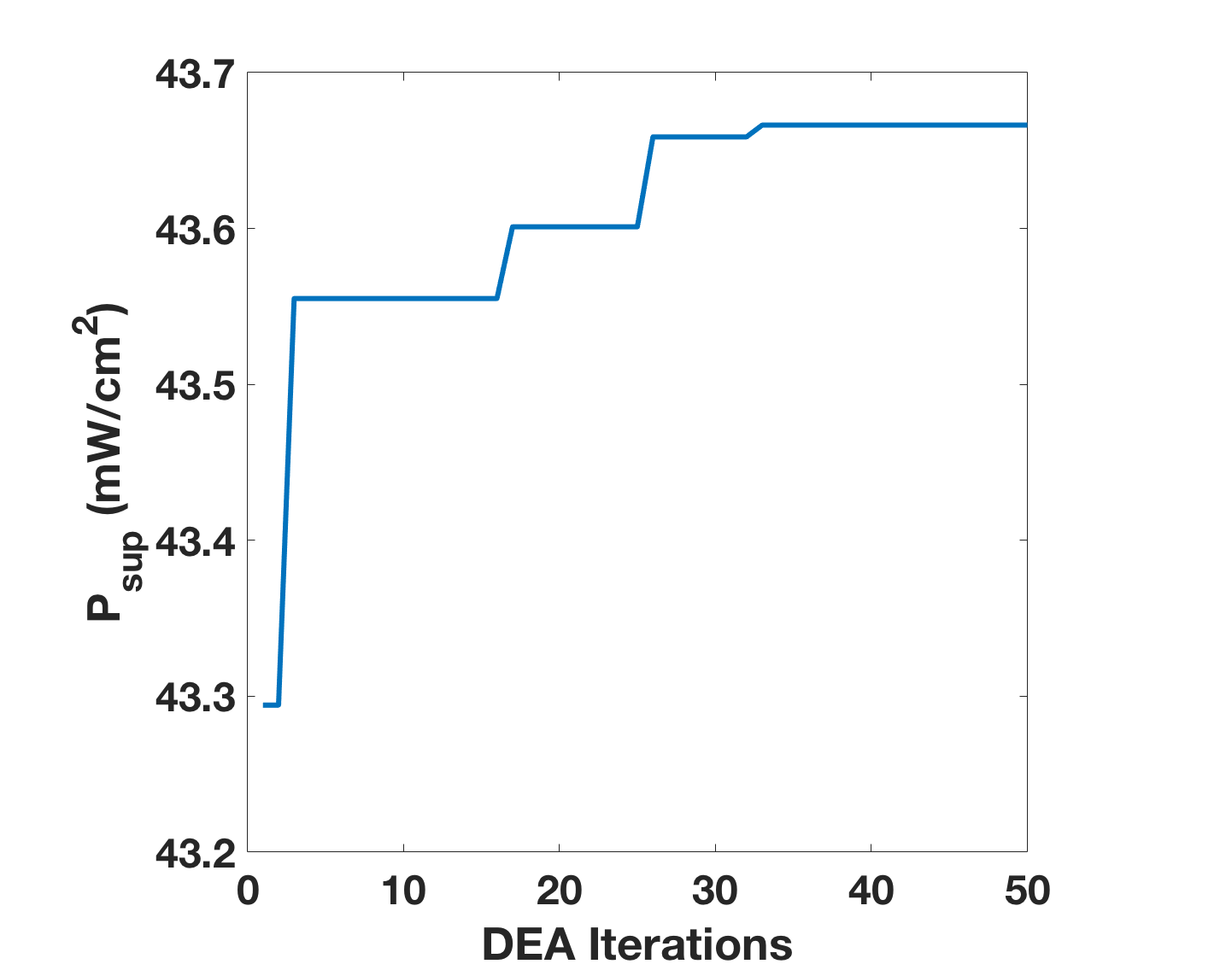
To ensure convergence of the optical short-circuit density, a representative configuration for the unit cell was used to determine an appropriate choice of and . We let vary in the set , and defined , where is the ceiling function. After determining that changed by for two successive values of and , the number of Fourier modes were fixed for all numerical results reported in this paper, and taken to be , . Since Eq. (16) has the charge-carrier generation rate integrated over the nine semiconductor layers, the susceptibility of to the effect of Gibbs’ phenomenon[6] on the electric field in the region is negligible. Hence, the electric field converges everywhere in the semiconductor layers, even for relatively small values of and . We performed 50 DEA iterations in the optimization exercise. Figure 5 shows the convergence of with the number of DEA iterations. We see that the best value of does not change after the first 32 DEA iterations. As with any stochastic optimization method, it is always possible that further iteration would result in improvement of the computed maximum power density.
4.4 Comparison to bi-sinusoidal PCBR
A third DEA-based optimization exercise was performed with the PCBR taken to be bi-sinusoidally corrugated [11]. The relative permittivity in the grating region is
| (18) |
with the corrugation-shape functions
| (19) | ||||
| (20) |
The DEA parameters were kept the same as in Sec. 4, and we set for the computation. The optimization exercise yielded an optimal configuration with nm, nm, nm, nm, eV, eV and eV. The maximal power density achieved was mW cm-2, which is slightly lower than mW cm-2 obtained for the hexagonally corrugated PCBR in Sec. 4.2. However, the average over all configurations visited by the DEA for the bi-sinusoidally corrugated PCBR is mW cm-2 but mW cm-2 for the hexagonally corrugated PCBR. There were many more configurations with relatively poor values for the hexagonal case.
5 Closing Remarks
As a model problem to demonstrate the practicability of the RCWA+DEA approach to design efficient optically absorbing 3D structures, optimal values of four geometric parameters and the bandgaps of three -layers were found for an idealized, multi-terminal, thin-film tandem solar cell comprising three -- junctions with a silver PCBR with hillock-shaped corrugations arranged on a hexagonal lattice. The figure of merit for the DEA was either (i) the optical short-circuit current density in Sec. 4.1 or (ii) the power density in Sec. 4.2. Thus, two different optimization exercises using the RCWA+DEA approach where performed.
As the optical short-circuit current density takes into account only the optical constitutive properties of the solar cell, maximization of that quantity resulted in a poor design. In particular, we determined that only the bandgap of the topmost -layer (i.e., ) was significant to the optimization of the optical short-circuit current density, and the remaining six parameters played minor roles. While photon absorption in the topmost -- junction was maximized thereby, this configuration would have poor electrical performance. This is because, when the thicknesses of the -layers were included in the optimization, the DEA simply focused on the maximization of those thicknesses. Although increasing those thicknesses can enhance light absorption, the electrical performance may be sacrificed, thereby reducing efficiency. The design of thin-film solar cells must balance optical and electrical performances [31, 32].
In order to avoid configurations with potentially poor electrical performance, we next used the power density—thereby weighting the optical short-circuit current density—as a new figure of merit. The resulting configuration was optimal with respect to all seven design parameters. Another optimization exercise was then performed on a similar tandem solar cell, but with a bi-sinusoidally corrugated PCBR. In this case the configurationally averaged power density tested by the DEA was about 10% higher than with the hexagonally corrugated PCBR. In the future, we plan to supplement the optical model by an electrical drift-diffusion model [32] and then optimize the overall electrical performance of the solar cell.
In closing, let us emphasize that the triple-junction tandem solar cell was chosen as a model problem to show here the capabilities of the RCWA+DEA approach developed for 3D optically absorbing structures. Our approach can be extended not only to other types of photovoltaic solar cells [33, 34] but also to optical absorbers [35, 36] with 3D morphology.
Note. This paper is substantially based on a paper titled, “Optimization of charge-carrier generation in amorphous-silicon thin-film tandem solar cell backed by two-dimensional metallic surface-relief grating,” presented
at the SPIE Optics and Photonics conference Next Generation Technologies for Solar Energy Conversion VIII, held August 5–11,
2017 in San Diego, California, United States.
Acknowledgments. The research of B. J. Civiletti, T. H. Anderson, and P. B. Monk is partially supported by the US National Science Foundation (NSF) under grant number DMS-1619904. The research of F. Ahmed and A. Lakhtakia is partially supported by the US NSF under grant number DMS-1619901. A. Lakhtakia thanks the Charles Godfrey Binder Endowment at the Pennsylvania State University for ongoing support of his research.
References
- [1] M. G. Moharam et al., “Formulation for stable and efficient implementation of the rigorous coupled-wave analysis of binary gratings,” J. Opt. Soc. Am. A 12, 1068–1076 (1995).
- [2] N. Chateau and J.-P. Hugonin, “Algorithm for the rigorous coupled-wave analysis of grating diffraction,” J. Opt. Soc. Am. A 11, 1321–1331 (1994).
- [3] P. Sheng, A. N. Bloch, and R. S. Stepleman, “Wavelength-selective absorption enhancement in thin-film solar cells,” Appl. Phys. Lett. 43, 579–581 (1983).
- [4] C. Heine and R. H. Morf, “Submicrometer gratings for solar energy applications,” Appl. Opt. 34, 2476–2482 (1995).
- [5] M. Solano et al., “Optimization of the absorption efficiency of an amorphous-silicon thin-film tandem solar cell backed by a metallic surface-relief grating,” Appl. Opt. 52, 966–979 (2013); erratum: 54, 398–399 (2015).
- [6] M. Weismann, D. F. G. Gallagher, and N. C. Panoiu, “Accurate near-field calculation in the rigorous coupled-wave analysis method,” J. Opt. (Bristol) 17, 125612 (2015).
- [7] M. V. Shuba et al., “Adequacy of the rigorous coupled-wave approach for thin-film silicon solar cells with periodically corrugated metallic backreflectors: spectral analysis,” J. Opt. Soc. Am. A 32, 1222–1230 (2015).
- [8] R. Storn and K. Price, “Differential evolution—a simple and efficient heuristic for global optimization over continuous spaces,” J. Global Optim. 11, 341–359 (1997).
- [9] K. Price, R. M. Storn, and J. A. Lampinen, Differential Evolution: A Practical Approach to Global Optimization, Springer, New York, NY, USA (2005).
- [10] M. Onishi, K. Crabtree, and R. A. Chipman, “Formulation of rigorous coupled-wave theory for gratings in bianisotropic media,” J. Opt. Soc. Am. A 28, 1747–1758 (2011).
- [11] F. Ahmad et al., “On optical-absorption peaks in a nonhomogeneous thin-film solar cell with a two-dimensional periodically corrugated metallic backreflector,” J. Nanophoton. 12(1), 016017 (2018).
- [12] B. J. Civiletti et al., “Optimization of charge-carrier generation in amorphous-silicon thin-film tandem solar cell backed by two-dimensional metallic surface-relief grating,” Proc. SPIE 10368, 1036809 (2017).
- [13] A. S. Ferlauto et al., “Analytical model for the optical functions of amorphous semiconductors from the near-infrared to ultraviolet: Applications in thin film photovoltaics,” J. Appl. Phys. 92, 2424–2436 (2002).
- [14] E. D. Palik (ed.), Handbook of Optical Constants of Solids, Academic Press, Boston, MA, USA (1985).
- [15] L. M. Anderson, “Harnessing surface plasmons for solar energy conversion,” Proc. SPIE 408, 172–178 (1983).
- [16] M. A. Green and S. Pillai, “Harnessing plasmonics for solar cells,” Nat. Photonics 6, 130–132 (2012).
- [17] M. Faryad and A. Lakhtakia, “Enhancement of light absorption efficiency of amorphous-silicon thin-film tandem solar cell due to multiple surface-plasmon-polariton waves in the near-infrared spectral regime,” Opt. Eng. 52, 087106 (2013); errata: 53, 129801 (2014).
- [18] S. Zhou et al., “Optimizing two-level hierarchical particles for thin-film solar cells,” Opt. Express 21, A285–A294 (2013).
- [19] A. Naqavi et al., “Enhanced light trapping in realistic thin film solar cells using one-dimensional gratings,” Proc. SPIE 8065, 80650A (2012).
- [20] L.C. Andreani, A. Bozzola, and M. Liscidini, “Light trapping in thin-film solar cells: towards the Lambertian limit,” Proc. SPIE 8438, 884380C (2012).
- [21] J. A. Polo Jr., T. G. Mackay, and A. Lakhtakia, Electromagnetic Surface Waves: A Modern Perspective, Elsevier, Waltham, MA, USA (2013).
- [22] National Renewable Energy Laboratory, Reference Solar Spectral Irradiance: Air Mass 1.5.
- [23] Y. Jaluria, Computer Methods for Engineering, Taylor & Francis, Washington, DC, USA (1996).
- [24] H. Hochstadt, Differential Equations: A Modern Approach, Dover Press, New York, NY, USA (1975).
- [25] R. Knobloch, J. Mlynek, and R. Srb, “Improving convergence properties of a differential evolution algorithm,” AIP Conf. Proc. 1789, 030005 (2016).
- [26] L. Liu et al., “Planar light concentration in micro-Si solar cells enabled by a metallic grating–photonic crystal architecture,” ACS Photonics 3(4), 604–610 (2016).
- [27] X.-Y. Gao, L. Liang, and Q.-G. Lin, “Analysis of the optical constants of aluminum-doped zinc-oxide films by using the single-oscillator model,” J. Korean Phys. Soc. 57, 710–714 (2010).
- [28] L. Vegard. “Die Röntgenstrahlen im Dienste der Erforschung der Materie,” Z. Kristallographie 67(1-6), 239–259 (1928).
- [29] N. Anttu et al., “Absorption and transmission of light in III–V nanowire arrays for tandem solar cell applications,” Nanotechnology 28, 205203 (2017).
- [30] J.-P. Colinge and C. A. Colinge, Physics of Semiconductor Devices, Kluwer Academic, New York, NY, USA (2002).
- [31] M. Faryad et al., “Optical and electrical modeling of an amorphous-silicon tandem solar cell with nonhomogeneous intrinsic layers and a periodically corrugated back-reflector,” Proc. SPIE 8823, 882306 (2013).
- [32] T. H. Anderson et al., “Combined optical-electrical finite-element simulations of thin-film solar cells with homogeneous and nonhomogeneous intrinsic layers,” J. Photon. Energy 6, 025502 (2016).
- [33] J. Zhu et al., “Nanodome solar cells with efficient light management and self-cleaning,” Nano Lett. 10, 2342–2348 (2010).
- [34] R. Kapadia et al., “Nanopillar photovoltaics: Materials, processes, and devices,” Nano Energy 1, 132–144 (2011).
- [35] N. Liu et al., “Infrared perfect absorber and its application as plasmonic sensor,” Nano Lett. 10, 1979–1984 (2010).
- [36] S. Butun and K. Aydin, “Structurally tunable resonant absorption bands in ultrathin broadband plasmonic absorbers,” Opt. Express 22, 19457–19468 (2014).