Efficient spin injection into graphene through trilayer hBN tunnel barriers
Abstract
We characterize the spin injection into bilayer graphene fully encapsulated in hBN using trilayer (3L) hexagonal boron nitride (hBN) tunnel barriers. As a function of the DC bias, the differential spin injection polarization is found to rise up to -60% at -250 mV DC bias voltage. We measure a DC spin polarization of 50%, a 30% increase compared to 2L-hBN. The large polarization is confirmed by local, two terminal spin transport measurements up to room temperature. We observe comparable differential spin injection efficiencies from Co/2L-hBN and Co/3L-hBN into graphene and conclude that possible exchange interaction between cobalt and graphene is likely not the origin of the bias dependence. Furthermore, our results show that local gating, arising from the applied DC bias is not responsible for the DC bias dependence. Carrier density dependent measurements of the spin injection efficiency are discussed, where we find no significant modulation of the differential spin injection polarization. We also address the bias dependence of the injection of in-plane and out-of-plane spins and conclude that the spin injection polarization is isotropic and does not depend on the applied bias.
I Introduction
Graphene is an ideal material for long distance spin transport experiments due to its low intrinsic spin-orbit coupling and outstanding electronic quality Huertas-Hernando et al. (2006); Han et al. (2014); Roche et al. (2015); Ingla-Aynés et al. (2016); Drögeler et al. (2016). Experimental results have shown that long spin relaxation lengths require the protection of the graphene channel from contamination (Ingla-Aynés et al., 2016; Drögeler et al., 2016; Zomer et al., 2012; Guimarães et al., 2014). The most effective way to achieve this is the encapsulation of graphene with hexagonal Boron Nitride (hBN), which substantially improved the spin transport properties Zomer et al. (2012); Guimarães et al. (2014); Drögeler et al. (2014); Ingla-Aynés et al. (2015); Drögeler et al. (2016); Gurram et al. (2016); Singh et al. (2016). Besides of the cleanliness of the channel, the efficient injection and detection of spins into graphene is an essential requirement to fabricate high performance devices. To circumvent the conductivity mismatch problem Schmidt et al. (2000), a tunnel barrier is employed to enhance the spin injection polarization Rashba (2000). While commonly used Al2O3 and TiO2 tunnel barriers yield typically spin polarizations below 10% Józsa et al. (2009). The use of crystalline MgO Han et al. (2010); Volmer et al. (2013, 2014), hBN Kamalakar et al. (2015, 2016); Gurram et al. (2017), amorphous carbon Neumann et al. (2013) or SrO Singh et al. (2017) as tunnel barrier has led to significant enhancements. In particular, the use of a 2L-hBN flake for spin injection gives rise to bias dependent differential spin injection polarizations p up to p = 70%, which is defined as the injected AC spin current is divided by the AC charge current iAC. Furthermore, 2L-hBN provides contact resistances in the range of 10 k, which can be close to the spin resistance of high quality graphene and affect spin transport Gurram et al. (2017). 3L-hBN tunnel barriers promise higher contact resistances, leaving the spin transport in 3L-hBN/graphene unaffected Kamalakar et al. (2016); Gurram et al. (2018).
While the underlying mechanism for the DC bias dependent spin injection is still unclear, ab initio calculations of cobalt separated from graphene by hBN show, that in the optimal case Co can induce an exchange interaction of 10 meV even through 2L-hBN into graphene Zollner et al. (2016), therefore, a comparison between hBN tunnel barriers of different thicknesses can give insight on the proximity effects between graphene and cobalt.
Here we show that 3L-hBN tunnel barriers increase the differential spin injection polarization into bilayer graphene (BLG) from a zero bias value of p = 20% up to values above p = -60% at negative DC bias. The DC spin injection polarization P, which is defined as the DC spin current Is divided by the DC charge current IDC, increases up to P = 50%, at a DC bias current of -2 A. This is a substantial advantage over 2L-hBN, which shows P 35%. The large DC spin polarization allows us to measure spin signals in a DC two terminal spin valve geometry up to room temperature. We show that the differential spin injection polarization is, contrary to Ringer et al. Ringer et al. (2018), independent of the carrier density. The rotation of the magnetization of the electrodes out-of-plane under a perpendicular magnetic field allows us to study the bias dependence of the spin injection polarization of out-of-plane spins (). We compare with the in-plane polarization and conclude that 1, independently of the applied DC bias.
II Sample preparation and contact characterization
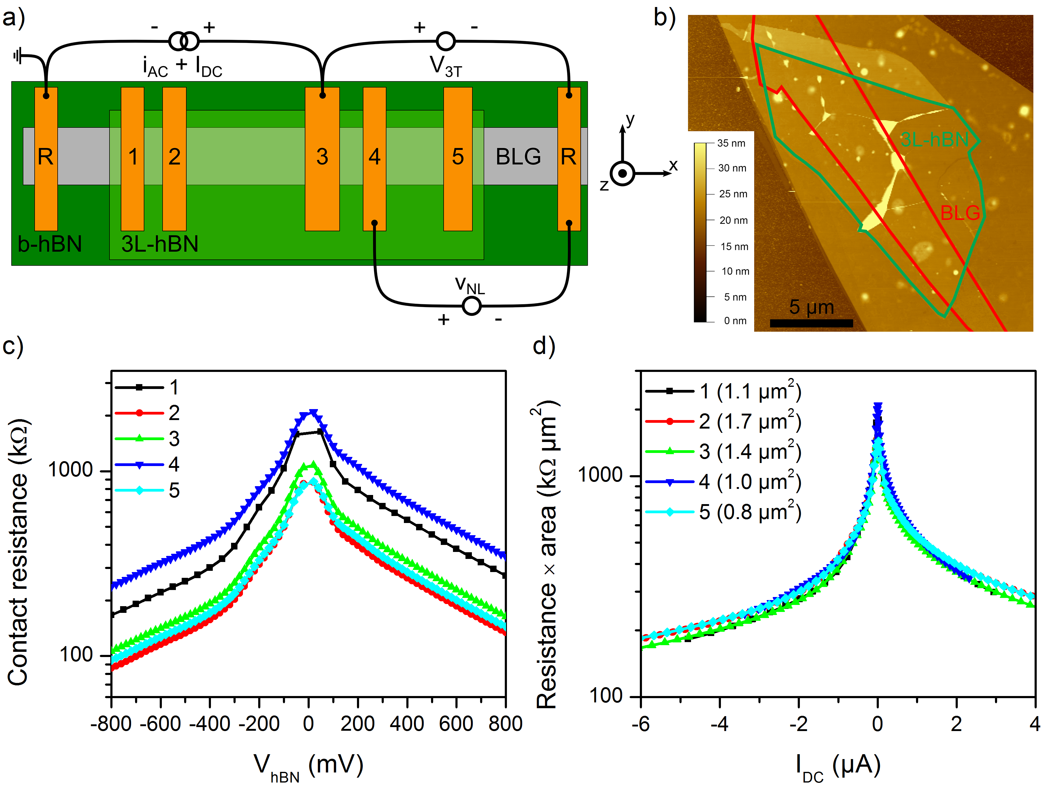
The device geometry is shown in Fig. 1a. BLG is encapsulated between a 5 nm thick bottom hBN and a 1.2 nm thick 3L-hBN flake, which acts as a tunnel barrier. The stack is deposited on a silicon oxide substrate with 90 nm oxide thickness, that is used to tune the carrier concentration in the graphene channel. This device has been used to study the spin lifetime anisotropy in BLG Leutenantsmeyer et al. (2018a). Unless noted, all measurements are carried out at T = 75 K to improve the signal to noise ratio. The atomic force microscopy image of the stack before the contact deposition is shown in Fig. 1b. The contact resistances are characterized by measuring the bias dependence in the three terminal geometry, Rc = V3T/IDC, and shown in Fig. 1c as a function of the voltage applied across the 3L-hBN tunnel barrier (V3T). The bias dependent contact resistances are normalized to the contact area and plotted as a function of the DC current IDC applied to the hBN barrier in Fig. 1d. To determine the spin transport properties of our device, we use the standard non-local geometry Jedema et al. (2001, 2002); Tombros et al. (2007), the circuit is shown in Fig. 1a. An AC charge current iAC is applied together with IDC between the injector and the left reference contact, which does not have any tunnel barrier and therefore does not inject spins efficiently. Because of the spin polarization of the cobalt/hBN contacts, the injected charge current is spin polarized and induces a spin accumulation into the channel. The spins diffuse in the BLG channel and are detected by a second cobalt/hBN contact in the non-local geometry.
III Spin transport at different DC bias currents
The different coercive fields of the cobalt contacts allow the separate switching of individual electrodes with an in-plane magnetic field and the measurement of the non-local resistance ( = vNL/iAC) in different magnetic configurations. The non-local spin valve is shown in Fig. 2a for different DC bias currents. The abrupt signal changes are caused by the switching of the contact magnetization, the magnetization configurations are indicated with arrows. The spin signal is determined by the difference between parallel (() = () and antiparallel (() = ()) configurations.
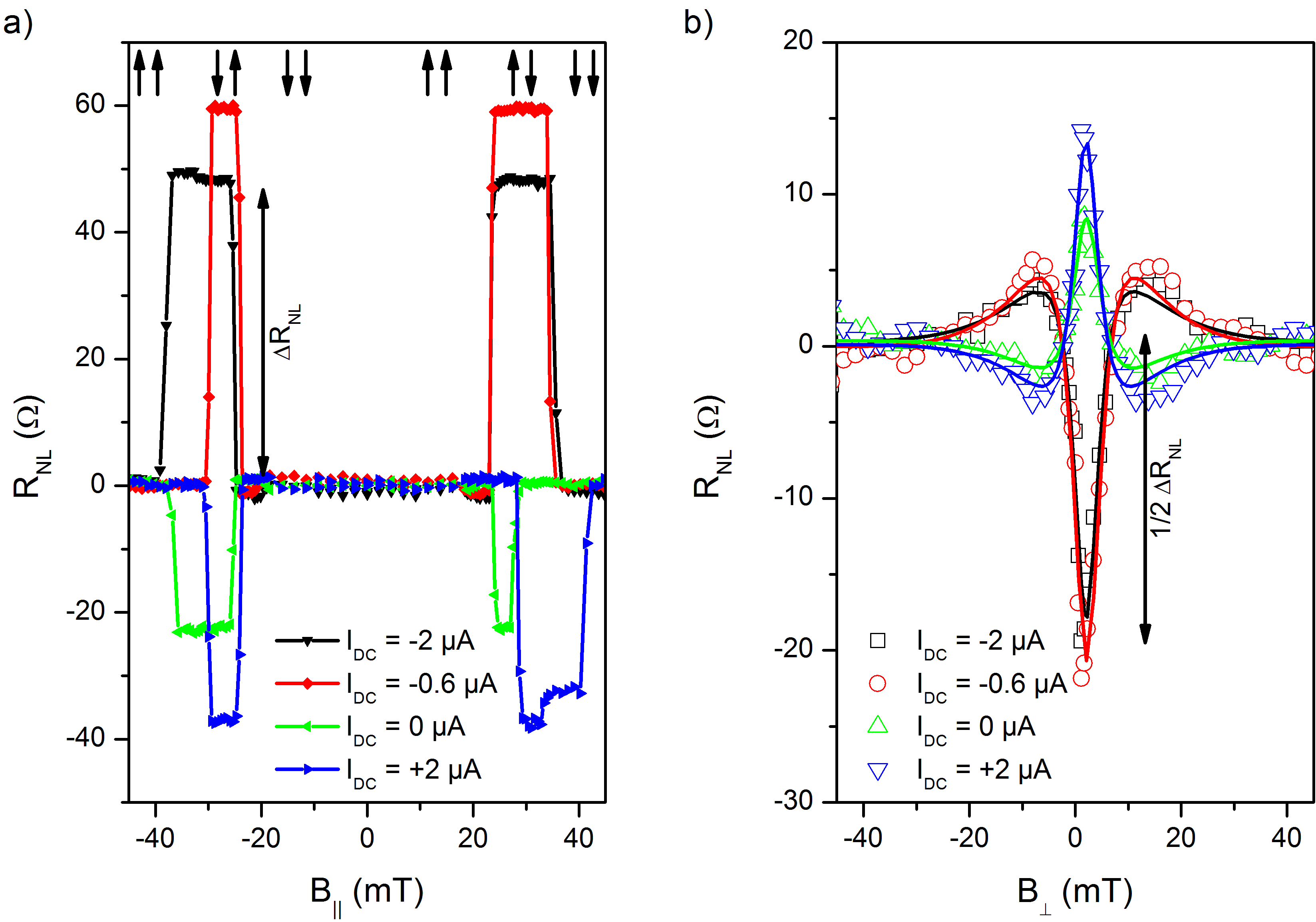
The most accurate way to characterize the spin transport properties of the channel is using spin precession, where the magnetic field is applied perpendicular to the BLG plane (), causing spins to precess in the x-y plane. By fitting to the Bloch spin diffusion equations, we extract the spin lifetime (), spin diffusion coefficient () and the average polarization of both electrodes (). The data is shown for different DC bias currents in Fig. 2b, the fitting curves are shown as solid lines. Note that the spin transport parameters in Table 1 are within the experimental uncertainty for all values. Therefore, we average , , and the spin relaxation length () over all four values and obtain = (1.9 0.2) ns, = (183 17) cm2/s and = = (5.8 0.6) m. These parameters are comparable to the ones reported in Ref. Gurram et al. (2018). We conclude that the change in contact resistance with does not affect the spin transport for values above 100 k. This is caused by the fact that the contact resistance remains clearly above the spin resistance of the channel Rs = /w 1.8 k, where is the graphene square resistance and w the graphene width Maassen et al. (2012).
| (A) | (km2) | () | (ns) | (m) |
|---|---|---|---|---|
| -2 | 280 | 208 25 | 2.1 0.2 | 6.4 1.6 |
| -0.6 | 760 | 177 21 | 1.7 0.2 | 5.5 1.2 |
| 0 | 2100 | 171 24 | 1.7 0.2 | 5.4 1.5 |
| +2 | 380 | 177 24 | 2.0 0.2 | 5.8 1.5 |
Note that the spin resistance of graphene can exceed 10 k in high quality devices. This is close to the contact resistance of biased 2L-hBN tunnel barriers, which typically range, depending IDC, between 5 k and 30 k Leutenantsmeyer et al. (2018b). Furthermore, the extended data sets discussed in the supplementary information and our analysis in Ref. Leutenantsmeyer et al. (2018a) confirm that contact induced spin backflow is not limiting spin transport for contact resistances above 100 k.
IV DC bias dependence of the differential spin injection efficiency
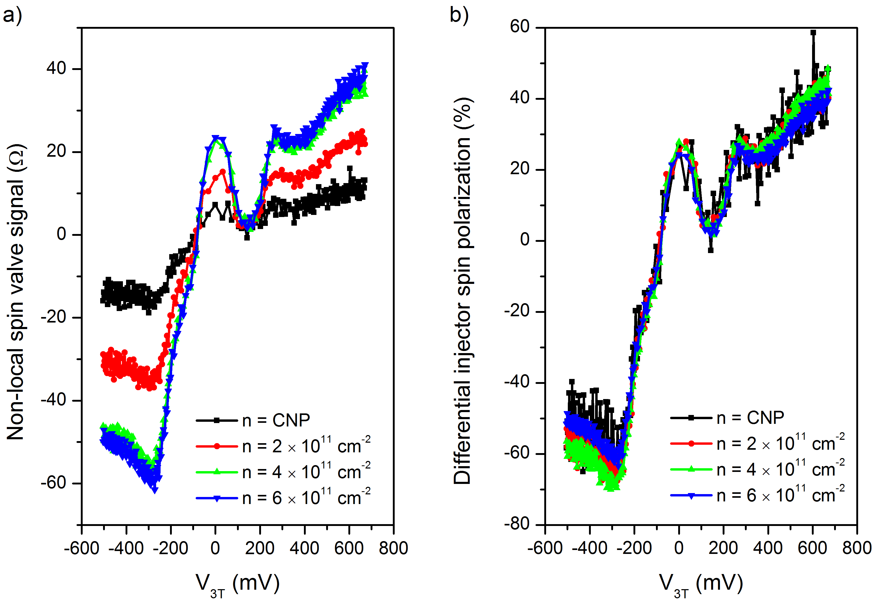
In Fig. 3a we show the non-local spin valve signal = - . For a comparison with 2L-hBN tunnel barriers, we calculate V3T, the voltage applied to the tunnel barrier, by using the current-voltage characteristics of each contact. To resolve small features in the bias dependence, we use measurement currents as low as iAC = 50 nA. As observed for 2L-hBN barriers Gurram et al. (2017); Leutenantsmeyer et al. (2018b), changes sign at V3T -100 mV, which we also observe with a 3L-hBN barrier. Our data also shows additional features: Firstly, shows a maximum at V3T -250 mV and decreases again for V3T -250 mV. In contrast, we observe a continuous increase for V3T +300 mV. Secondly, we observe a peak at zero V3T, indicating that the polarization of Co/3L-hBN at zero DC bias is higher than in Co/2L-hBN. Note that 2L-hBN devices in Ref. Leutenantsmeyer et al. (2018b) show also these small features around zero DC bias (Fig. 4b).
To calculate the polarization of the Co/hBN interface from , we use:
| (1) |
where and are the differential injector and detector spin polarizations, and the separation between injector and detector. An overview of all extracted spin transport parameters is shown in the supplementary information. Following this procedure for IDC = 0 at different configurations we obtain the unbiased spin polarizations of all contacts of p1 = 24%, p2 = 23%, p3 = 30%, p4 = 36%, and p5= 38%. Since does not depend on the DC bias, which is applied to the injector only, we can calculate the bias dependence of (Fig. 3b). The absolute sign of p cannot be determined from spin transport measurements Gurram et al. (2017), and we define p to be positive for IDC = 0.
Note that the slope observed in Fig. 3b is in qualitative agreement with the ab-initio calculations by Piquemal-Banci et al. Piquemal-Banci et al. (2018) for chemisorbed cobalt on hBN, suggesting that the observed DC bias dependence arises from the Co/hBN interface and not from proximity coupling between cobalt and graphene.
We conclude that (IDC) can reach values comparable to 2L-hBN tunnel barriers. Moreover, the comparison between different carrier concentrations shows that the spin injection polarization does not depend of the carrier density, even at the charge neutrality point. This also indicates that local spin drift in the barrier arising from pinholes is not responsible for the bias dependence. The drift velocity is inversely proportional to the carrier density, and therefore, the effect of spin drift is the largest near the neutrality point Ingla-Aynés et al. (2016). Furthermore, if charge carrier drift in the channel would be relevant, the measured Hanle curves would widen Huang and Appelbaum (2008). Consequently, the extracted spin lifetimes would decrease with increasing IDC, which we do not observe here. Furthermore, our IDC is at most 2 A, whereas a sizable drift effect requires larger charge currents Ingla-Aynés et al. (2016). Local charge carrier drift at the injector, caused by pinholes in the barrier, was used to explain a modulation of the spin injection polarization Józsa et al. (2009). From our measurements we can exclude this mechanism as origin due to the negligible modulation of the spin injection polarization with n. Moreover, we use crystalline hBN as tunnel barrier, which has the advantage over evaporated barriers that pinholes are not expected to be present.
V Calculation of the DC spin polarization
For practical applications, a large DC spin polarization P is required. Using the differential spin polarization , we can calculate P via Gurram et al. (2017):
| (2) |
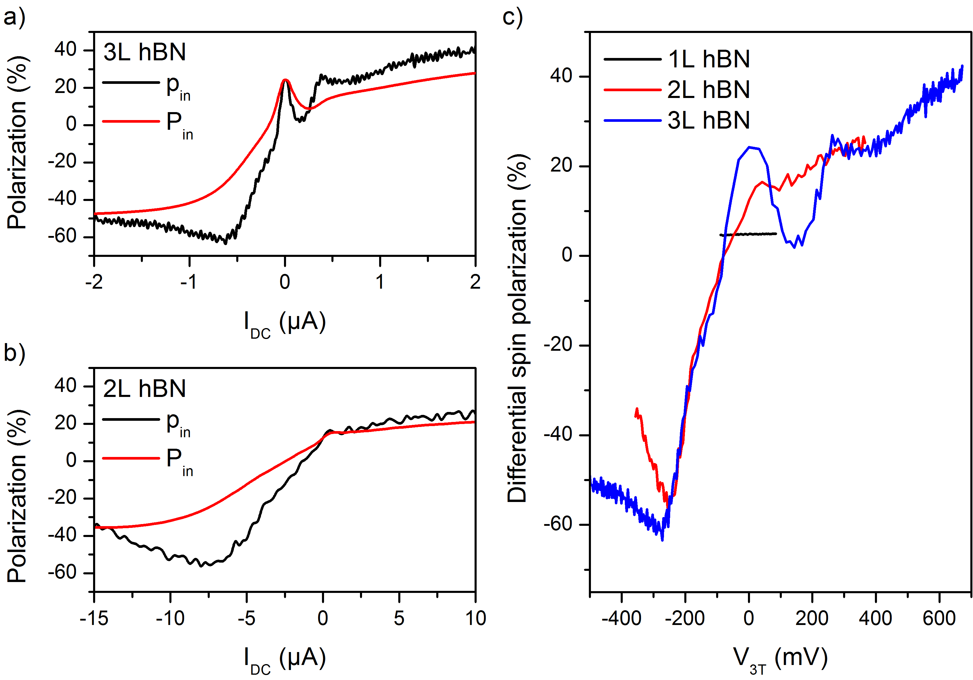
The results obtained for 3L- and 2L-hBN barriers using this procedure are shown in Fig. 4a and 4b. The DC spin polarization of 3L-hBN rises close to 50%, whereas 2L-hBN yield only up to 35%. Measurements on vertical tunnel junctions with 1L- and 2L-hBN tunnel barriers reported a spin polarization of 1% (1L) and 12% (2L) Dankert et al. (2015); Asshoff et al. (2017); Piquemal-Banci et al. (2018). This underlines the potential of cobalt/3L-hBN contacts for highly efficient spin injection into graphene.
The comparison of the differential spin polarization of 1L-, 2L- and 3L-hBN/Co contacts is shown in Fig. 4c. In the case of 1L-hBN, the polarization remains constant ( 5%), mostly independent of the applied V3T, and clearly below the values of 2L- and 3L-hBN barriers. However, the comparison of 2L- and 3L-hBN yields comparable differential spin polarizations, whereas the electric fields underneath the contacts, which arise from V3T, change from 1L- to 3L-hBN by a factor of 3. Therefore, local gating underneath the contacts can also be excluded as origin of the bias dependence. The effect of quantum capacitance is discussed in the supplementary information.
Zollner et al. Zollner et al. (2016) calculated the exchange coupling between cobalt and graphene separated by 1L- to 3L-hBN. Interestingly, they reported a spin splitting of up to 10 meV in when cobalt and graphene are separated by 2L-hBN. For 3L-hBN, this splitting decreases to 18 eV. Since we observe very comparable results between 3L-hBN and 2L-hBN, we conclude that proximity induced exchange splitting is most likely not the origin for the DC bias dependent spin injection efficiency in Co/hBN/graphene.
VI Isotropy of the spin injection efficiency
By applying a large 1.2 T, we can rotate the cobalt magnetization close to out-of-plane and characterize the spin injection efficiency of 3L-hBN tunnel barrier for out-of-plane spins. This measurement technique was used to determine the spin lifetime anisotropy of graphene Tombros et al. (2008), which can be also measured using oblique spin precession with lower applied magnetic fields Raes et al. (2016, 2017); Leutenantsmeyer et al. (2018a). By comparing both results, we can separate the anisotropy of the BLG channel from the anisotropy of the spin injection and detection polarization.
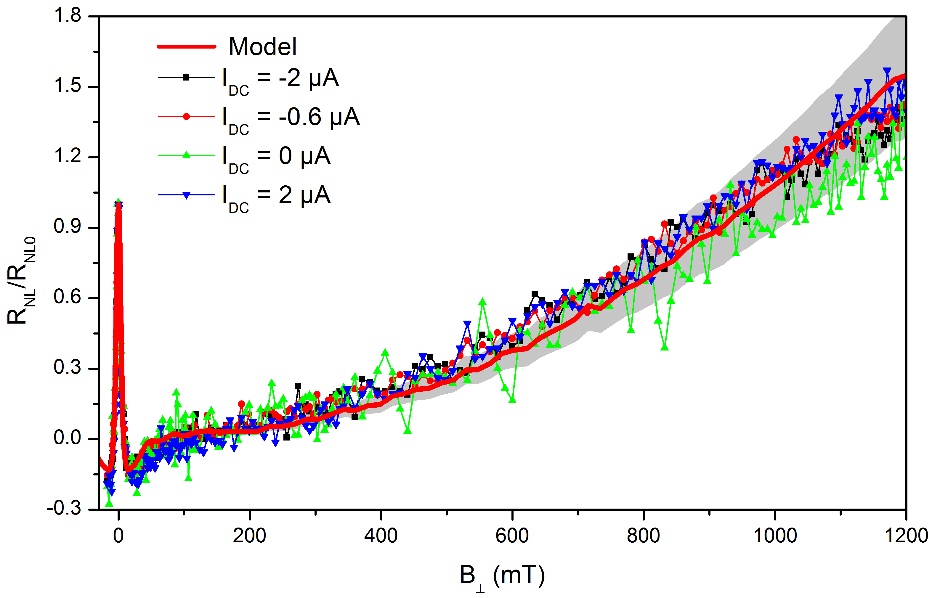
Fig. 5 shows the Hanle curves measured at a carrier concentration of n = 6 1011 cm-2, which is the highest density accessible in our device and has been chosen to minimize the effect of magnetoresistance and the spin lifetime anisotropy of the BLG channel. The data is normalized to = ( = 0 T), the gray shaded area is determined by the uncertainty of the extracted spin lifetime anisotropy. The normalized measurements at different IDC overlap each other, which indicates that is independent of .
We model the spin transport using the Bloch equations for anisotropic spin transport as discussed in Ref. Leutenantsmeyer et al. (2018a). Additionally, we include the rotation of the contact magnetization, which we extract from anisotropic magnetoresistance measurements, shown in the supplementary information. The good agreement between the experimental data and our model suggests that the spin injection polarization is isotropic, and, hence, .
VII Two terminal DC spin transport measurements up to room temperature
Lastly, we use the large DC spin polarization of our device to measure spin transport in a local two terminal geometry, which is especially interesting for applications. For this experiment we source a DC current () and measure simultaneously the DC voltage VDC between Contact 2 and Contact 1. The local, two terminal signal is R2T = VDC/, with the spin signal = is 162 at = -2 A 75 at = +1 A.
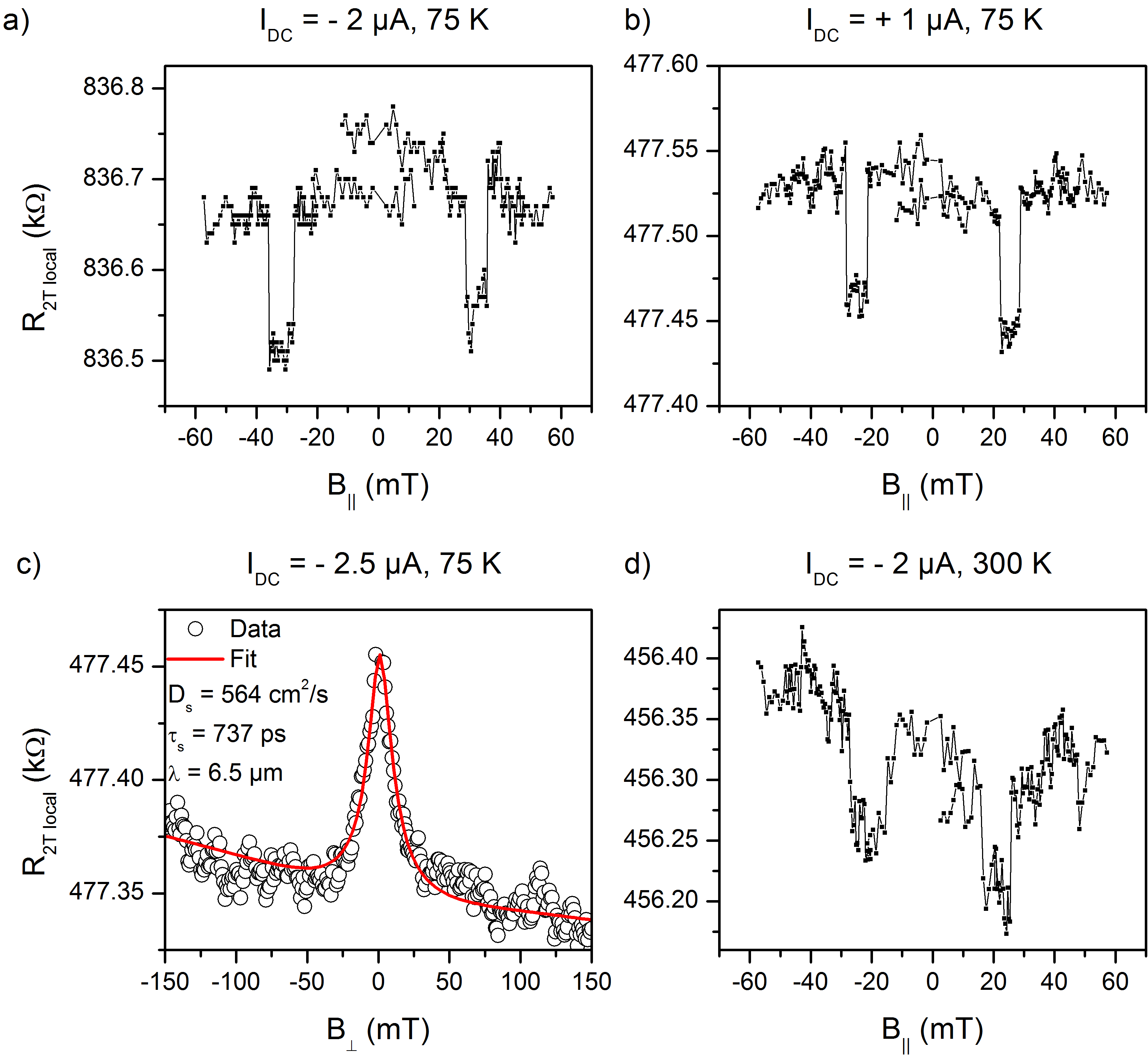
A measurement of spin precession between Contact 3 and Contact 2 is shown in Fig. 6c. We observe a clear Hanle curve and fit the data with = (740 60) ps, = (560 70) cm2/s and calculate = 6.5 m. Note that the change of these values compared to Table 1 was caused by an exposure of the sample to air. Using the spin polarization of the biased contacts and the extracted spin relaxation length, we can calculate the expected local 2T spin valve signal Gurram et al. (2017):
| (3) |
where the indexes A and B denote both contacts at the bias . We calculate using the spin polarization values = -177 at = -2 A and = -108 at = +1 A, which is in agreement with the measured data in Fig. 6a and 6b of 162 and 80 .
The measurement of at room temperature is shown in Fig. 6c. is at room temperature 100 and clearly present, which indicates no dramatic change of the DC spin polarization with increasing temperature. These results underline the relevance of 3L-hBN barriers for graphene spintronics.
VIII Summary
In conclusion, we have shown that 3L-hBN tunnel barriers provide a large, tunable spin injection efficiency from cobalt into graphene. The zero bias spin injection polarization is between 20% and 30%, and the differential spin injection polarization can increase to -60% by applying a negative DC bias. The resulting DC spin polarization of up to 50% allows spin transport measurements in a DC two terminal configuration up to room temperature. We study the n dependence of the spin injection polarization and find that it does not depend on n. From a comparison between 3L- and 2L-hBN, we observe that the DC bias dependence scales with the voltage and not the electric field, indicating that local gating is not the dominant mechanism. We also compare the spin injection polarization for in-plane and out-of-plane spins and find that it is isotropic and that is independent of the applied DC bias.
During the preparation of this manuscript we became aware of a related work Zhu et al. (2018), where also a DC bias dependent spin signal is reported in Co/SrO/graphene heterostructures. Furthermore, the authors also exclude carrier drift as origin.
Acknowledgements
We acknowledge the fruitful discussions with A.A. Kaverzin and technical support from H. Adema, J.G. Holstein, H.M. de Roosz, T.J. Schouten, and H. de Vries. This project has received funding from the European Union’s Horizon 2020 research and innovation program under the grant agreements 696656 and 785219 (‘Graphene Flagship’ Core 1 and 2), the Marie Curie initial training network ‘Spinograph’ (grant agreement 607904) and the Spinoza Prize awarded to B.J. van Wees by the ‘Netherlands Organization for Scientific Research’ (NWO).
Supplementary Information
S1 Fabrication details
The 3L-hBN/bilayer graphene (BLG)/bottom-hBN stack is fabricated using the scotch tape technique to exfoliate hBN from hBN powder (HQ Graphene) and graphene from HOPG (ZYA grade, HQ Graphene). The materials are stacked using a polycarbonate based dry transfer technique Zomer et al. (2014). The transfer polymer is removed in chloroform and the sample is annealed for one hour in Ar/H2. PMMA is spun on the sample and contacts are exposed using e-beam lithography. The sample is developed in MIBK:IPA and 65 nm Co and a 5 nm Al capping layer are deposited. The PMMA mask is removed in warm acetone. The sample is bonded on a chip carrier and loaded into a cryostat where the sample space is evacuated below 10-6 mbar.
S2 Determination of the unbiased contact spin polarization
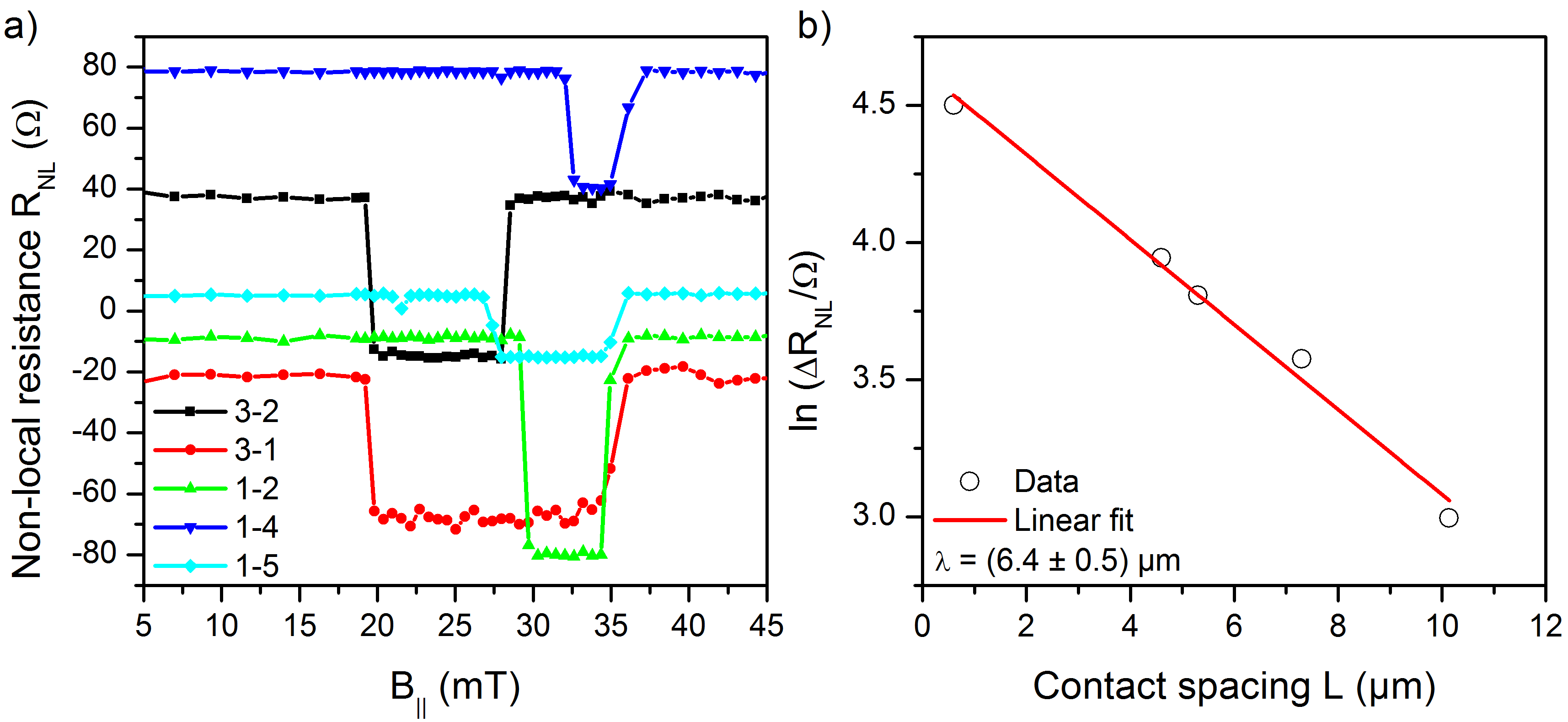
Fig. S1 shows the non-local spin valve measurement obtained from all different contact combinations. To calculate the unbiased spin polarization of each contact, we apply iAC = 50 nA to the injector and obtain the values in Table 1. The measurement is done without any DC bias current and back gate voltage applied, = 0, the corresponding carrier concentration is 4 cm-2.
To calculate the spin polarization of each contact, we use equation S1:
| (S1) |
where is the spin signal extracted from Fig. S1a, w = 3 m the width of the BLG and the square resistance of the BLG. The results are shown in Table 1.
| Injector | Detector | () | d (m) |
|---|---|---|---|
| 3 | 2 | 52 | 4.6 |
| 3 | 1 | 48 | 5.3 |
| 1 | 2 | 89 | 0.6 |
| 1 | 4 | 40 | 7.3 |
| 1 | 5 | 21 | 11.1 |
S3 Extraction of the magnetization rotation through AMR measurements
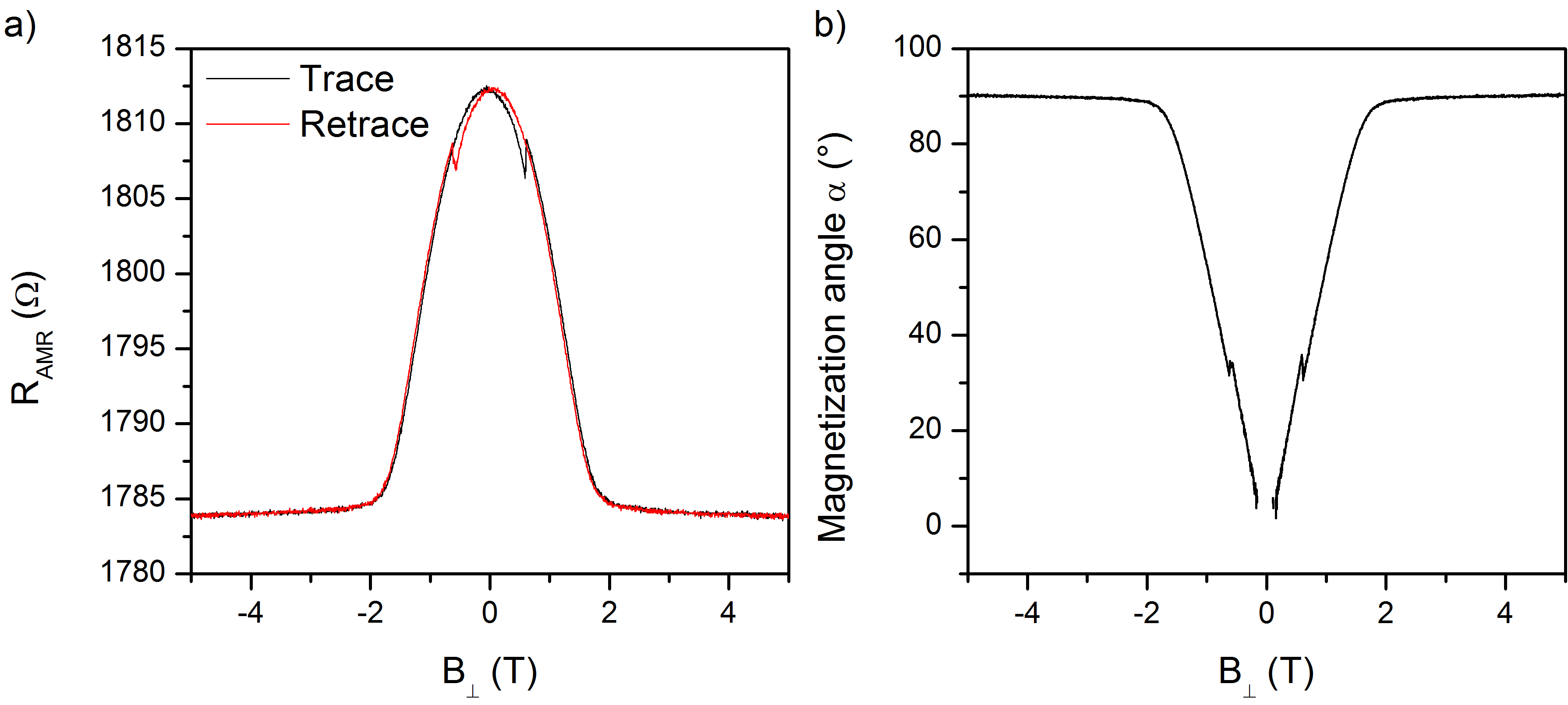
To accurately model the dependence of on , we measure the anisotropic magnetoresistance (AMR) effect, shown in Fig. S2a. The angle of the cobalt magnetization can be calculated at any given via Benítez et al. (2017):
| (S2) |
The calculated magnetization angle is shown in Fig. S2b and used to model the spin precession curves in the main text.
S4 Full set of spin transport parameters
Table 2 contains an overview of the full set of spin transport measurements using Contact 1 as injector and Contact 5 as detector. For each applied gate voltage, all spin transport parameters are within the experimental uncertainty, implying the independence of and on .
| (A) | (V) | () | (cm2/s) | (ns) | (m) |
|---|---|---|---|---|---|
| -2 | -2 | 1600 | 112 27 | 1.5 0.3 | 4.1 1.8 |
| -0.6 | -2 | 1600 | 114 24 | 1.4 0.3 | 4.0 1.6 |
| 0 | -2 | 1600 | 138 43 | 1.6 0.5 | 4.8 2.8 |
| 2 | -2 | 1600 | 86 21 | 1.0 0.3 | 2.9 1.3 |
| -2 | -1 | 1400 | 133 22 | 1.7 0.3 | 4.8 1.5 |
| -0.6 | -1 | 1400 | 140 20 | 1.7 0.3 | 4.9 1.3 |
| 0 | -1 | 1400 | 160 40 | 1.8 0.4 | 5.4 2.5 |
| 2 | -1 | 1400 | 137 22 | 1.8 0.3 | 5.0 1.5 |
| -2 | 0 | 900 | 202 26 | 2.0 0.3 | 6.4 1.6 |
| -0.6 | 0 | 900 | 176 21 | 1.7 0.2 | 5.5 1.2 |
| 0 | 0 | 900 | 170 24 | 1.7 0.3 | 5.4 1.5 |
| 2 | 0 | 900 | 174 24 | 1.9 0.3 | 5.8 1.5 |
| -2 | 1 | 750 | 226 24 | 2.2 0.2 | 7.1 1.4 |
| -0.6 | 1 | 750 | 230 25 | 1.8 0.2 | 6.5 1.3 |
| 0 | 1 | 750 | 214 27 | 1.8 0.2 | 6.1 1.5 |
| 2 | 1 | 750 | 222 25 | 2.1 0.2 | 6.8 1.4 |
S5 Quantum capacitance correction to bias-induced gating
A gate voltage does not only apply an electric field to the graphene channel but also tunes the Fermi energy (EF). This effect is called quantum capacitance correction and becomes relevant when the geometrical capacitance of the gate is very high, or the density of states of the channel is small. The quantum capacitance correction is calculated via Braga et al. (2012):
| (S3) |
where Vc denotes the voltage applied to the contact, the hBN tunnel barrier thickness, the electron charge, the vacuum permittivity, and the relative permittivity of hBN.
| (mV) | (nm) | (cm-2) | (cm-2) | |
|---|---|---|---|---|
| 300 | 3.52 | 1.2 (3L) | 3.35 | 4.86 |
| 300 | 3.44 | 0.7 (2L) | 4.78 | 8.15 |
The Fermi energy in the conduction band of BLG is determined by McCann and Koshino (2013):
| (S4) |
where is the interlayer hopping constant, the reduced Plank constant, and m/s the Fermi velocity in graphene.
Using Equation S3 and Equation S4, we calculate the carrier density for a DC bias of 300 mV in Table 3, assuming that the charge neutrality point lies at zero DC bias. We find that the quantum capacitance can have a significant effect on the carrier density compared to classical gating .
In conclusion, we find a substantial quantum capacitance correction. However, even with the quantum correction applied, the difference in the carrier concentration of 2L- and 3L-hBN is 30%. Consequently, we can still exclude local gating as origin of the DC bias dependence.
References
- Huertas-Hernando et al. (2006) D. Huertas-Hernando, F. Guinea, and A. Brataas, Physical Review B 74 (2006).
- Han et al. (2014) W. Han, R. K. Kawakami, M. Gmitra, and J. Fabian, Nature Nanotechnology 9, 794 (2014).
- Roche et al. (2015) S. Roche, J. Åkerman, B. Beschoten, J.-C. Charlier, M. Chshiev, S. P. Dash, B. Dlubak, J. Fabian, A. Fert, M. H. D. Guimarães, F. Guinea, I. Grigorieva, C. Schönenberger, P. Seneor, C. Stampfer, S. O. Valenzuela, X. Waintal, and B. J. van Wees, 2D Materials 2, 030202 (2015).
- Ingla-Aynés et al. (2016) J. Ingla-Aynés, R. J. Meijerink, and B. J. van Wees, Nano Letters 16, 4825 (2016).
- Drögeler et al. (2016) M. Drögeler, C. Franzen, F. Volmer, T. Pohlmann, L. Banszerus, M. Wolter, K. Watanabe, T. Taniguchi, C. Stampfer, and B. Beschoten, Nano Letters 16, 3533 (2016).
- Zomer et al. (2012) P. J. Zomer, M. H. D. Guimarães, N. Tombros, and B. J. van Wees, Physical Review B 86, 2 (2012).
- Guimarães et al. (2014) M. H. D. Guimarães, P. J. Zomer, J. Ingla-Aynés, J. C. Brant, N. Tombros, and B. J. van Wees, Physical Review Letters 113, 1 (2014).
- Drögeler et al. (2014) M. Drögeler, F. Volmer, M. Wolter, B. Terrés, K. Watanabe, T. Taniguchi, G. Güntherodt, C. Stampfer, and B. Beschoten, Nano Letters 14, 6050 (2014).
- Ingla-Aynés et al. (2015) J. Ingla-Aynés, M. H. D. Guimarães, R. J. Meijerink, P. J. Zomer, and B. J. van Wees, Physical Review B 92, 1 (2015).
- Gurram et al. (2016) M. Gurram, S. Omar, S. Zihlmann, P. Makk, C. Schönenberger, and B. J. van Wees, Physical Review B 93, 115441 (2016).
- Singh et al. (2016) S. Singh, J. Katoch, J. Xu, C. Tan, T. Zhu, W. Amamou, J. Hone, and R. K. Kawakami, Applied Physics Letters 109, 122411 (2016).
- Schmidt et al. (2000) G. Schmidt, L. W. Molenkamp, A. T. Filip, and B. J. van Wees, Physical Review B 62, R4790 (2000).
- Rashba (2000) E. I. Rashba, Physical Review B 62, 267 (2000).
- Józsa et al. (2009) C. Józsa, M. Popinciuc, N. Tombros, H. T. Jonkman, and B. J. van Wees, Physical Review B 79, 081402 (2009).
- Han et al. (2010) W. Han, K. Pi, K. M. McCreary, Y. Li, J. J. I. Wong, A. G. Swartz, and R. K. Kawakami, Physical Review Letters 105, 3 (2010).
- Volmer et al. (2013) F. Volmer, M. Drögeler, E. Maynicke, N. Von Den Driesch, M. L. Boschen, G. Güntherodt, and B. Beschoten, Physical Review B 88, 161405 (2013).
- Volmer et al. (2014) F. Volmer, M. Drögeler, E. Maynicke, N. Von Den Driesch, M. L. Boschen, G. Güntherodt, C. Stampfer, and B. Beschoten, Physical Review B 90, 165403 (2014).
- Kamalakar et al. (2015) M. V. Kamalakar, A. Dankert, J. Bergsten, T. Ive, and S. P. Dash, Scientific Reports 4, 6146 (2015).
- Kamalakar et al. (2016) M. V. Kamalakar, A. Dankert, P. J. Kelly, and S. P. Dash, Scientific Reports 6, 21168 (2016).
- Gurram et al. (2017) M. Gurram, S. Omar, and B. van Wees, Nature Communications 8, 248 (2017).
- Neumann et al. (2013) I. Neumann, M. V. Costache, G. Bridoux, J. F. Sierra, and S. O. Valenzuela, Applied Physics Letters 103, 112401 (2013).
- Singh et al. (2017) S. Singh, J. Katoch, T. Zhu, R. J. Wu, A. S. Ahmed, W. Amamou, D. Wang, K. A. Mkhoyan, and R. K. Kawakami, Nano Letters 17, 7578 (2017).
- Gurram et al. (2018) M. Gurram, S. Omar, and B. J. van Wees, 2D Materials 5, 032004 (2018).
- Zollner et al. (2016) K. Zollner, M. Gmitra, T. Frank, and J. Fabian, Physical Review B 94, 1 (2016).
- Ringer et al. (2018) S. Ringer, M. Rosenauer, T. Völkl, M. Kadur, F. Hopperdietzel, D. Weiss, and J. Eroms, (2018), 1803.07911 .
- Leutenantsmeyer et al. (2018a) J. C. Leutenantsmeyer, J. Ingla-Aynés, J. Fabian, and B. J. van Wees, (2018a), arXiv:1805.12420 .
- Jedema et al. (2001) F. J. Jedema, A. T. Filip, and B. J. van Wees, Nature 410, 345 (2001).
- Jedema et al. (2002) F. J. Jedema, H. B. Heersche, A. T. Filip, J. J. A. Baselmans, and B. J. van Wees, Nature 416, 713 (2002).
- Tombros et al. (2007) N. Tombros, C. Jozsa, M. Popinciuc, H. T. Jonkman, and B. J. van Wees, Nature 448, 571 (2007).
- Maassen et al. (2012) T. Maassen, I. J. Vera-Marun, M. H. D. Guimarães, and B. J. van Wees, Physical Review B 86, 235408 (2012).
- Leutenantsmeyer et al. (2018b) J. C. Leutenantsmeyer, T. Liu, M. Gurram, A. A. Kaverzin, and B. J. van Wees, (2018b), arXiv:1807.08481 .
- Piquemal-Banci et al. (2018) M. Piquemal-Banci, R. Galceran, F. Godel, S. Caneva, M.-B. Martin, R. S. Weatherup, P. R. Kidambi, K. Bouzehouane, S. Xavier, A. Anane, F. Petroff, A. Fert, S. Mutien-Marie Dubois, J.-C. Charlier, J. Robertson, S. Hofmann, B. Dlubak, and P. Seneor, ACS Nano 12, 4712 (2018).
- Huang and Appelbaum (2008) B. Huang and I. Appelbaum, Physical Review B 77, 1 (2008).
- Dankert et al. (2015) A. Dankert, M. Venkata Kamalakar, A. Wajid, R. S. Patel, and S. P. Dash, Nano Research 8, 1357 (2015).
- Asshoff et al. (2017) P. U. Asshoff, J. L. Sambricio, A. P. Rooney, S. Slizovskiy, A. Mishchenko, A. M. Rakowski, E. W. Hill, A. K. Geim, S. J. Haigh, V. I. Fal’Ko, I. J. Vera-Marun, and I. V. Grigorieva, 2D Materials 4 (2017), 10.1088/2053-1583/aa7452.
- Tombros et al. (2008) N. Tombros, S. Tanabe, A. Veligura, C. Jozsa, M. Popinciuc, H. T. Jonkman, and B. J. van Wees, Physical Review Letters 101, 2 (2008).
- Raes et al. (2016) B. Raes, J. E. Scheerder, M. V. Costache, F. Bonell, J. F. Sierra, J. Cuppens, J. van de Vondel, and S. O. Valenzuela, Nature Communications 7, 11444 (2016).
- Raes et al. (2017) B. Raes, A. W. Cummings, F. Bonell, M. V. Costache, J. F. Sierra, S. Roche, and S. O. Valenzuela, Physical Review B 95, 1 (2017).
- Zhu et al. (2018) T. Zhu, S. Singh, J. Katoch, H. Wen, K. Belashchenko, I. Žutic, and R. K. Kawakami, (2018), arXiv:1806.06526 .
- Zomer et al. (2014) P. J. Zomer, M. H. D. Guimarães, J. C. Brant, N. Tombros, and B. J. van Wees, Applied Physics Letters 105, 013101 (2014).
- Benítez et al. (2017) L. Benítez, J. Sierra, W. Savero Torres, A. Arrighi, F. Bonell, M. Costache, and S. Valenzuela, Nature Physics 14, 1 (2017).
- Braga et al. (2012) D. Braga, I. Gutieérrez Lezama, H. Berger, and A. F. Morpurgo, Nano Letters 12, 5218 (2012).
- McCann and Koshino (2013) E. McCann and M. Koshino, Reports on Progress in Physics 76, 056503 (2013).
- Laturia et al. (2018) A. Laturia, M. L. van de Put, and W. G. Vandenberghe, npj 2D Materials and Applications 2, 6 (2018).