Layer -projection and unfolding electronic bands at interfaces
Abstract
The -projection method provides an approach to separate the contributions from different constituents in heterostructure systems, and can act as an aid to connect the results of experiments and calculations. We show that the technique can be used to “unfold” the calculated electronic bands of interfaces and supercells, and provide local band structure by integrating the projected states over specified regions of space, a step that can be implemented efficiently using fast Fourier transforms. We apply the method to investigate the effects of interfaces in heterostructures consisting of a graphene bilayer on H-saturated SiC(0001), BAs monolayer on the ferromagnetic semiconductor CrI3, silicene on Ag(111), and to the Bi2Se3 surface. Our results reveal that the band structure of the graphene bilayer around the Dirac point is strongly dependent on the termination of SiC(0001): on the C-face, the graphene is -doped and a gap of 0.13 eV is opened, whereas on the Si-face, the graphene is essential unchanged and neutral. We show that for BAs/CrI3, the magnetic proximity effect can effectively induce a spin splitting up to about 50 meV in BAs. For silicene/Ag(111), our calculations reproduce the angle-resolved photoemission spectroscopy results, including linearly dispersing bands at the edge of the first Brillouin zone of Ag(111); although these states result from the interaction between the silicene overlayer and the substrate, we demonstrate that they are not Dirac states.
pacs:
71.20.-b,73.20.-r,73.22.PrI INTRODUCTION
Doping has been an important means of tailoring electronic properties of materials, and exploring novel physical phenomena, such as doping Mott insulators to obtain high Tc superconductors,Bednorz and Müller (1986) doping Ge by Sn to obtain direct semiconductors, Gupta et al. (2013) and realizing quantum anomalous Hall effect in topological insulators by doping magnetic impurities.Yu et al. (2010); Chang et al. (2013) As the thickness of materials approach the atomic limit, the interface between the material and the substrate plays a critical role in determining its atomic structure and electronic properties. The increased interest in interface effects has motivated in part by experimental realization of stable monolayer systems such as graphene and transition-metal dichalcogenides (TMDs). For example, the magnetic proximity effect has been used to manipulate spin polarization, spin-valley polarization, and explore quantum anomalous Hall effect in the monolayers by placing them onto the surface of magnetic semiconductors.Yang et al. (2013); Wei et al. (2016); Qi et al. (2015); Zhang et al. (2016); Qiao et al. (2014); Wang et al. (2015); Zhang et al. (2015) The research has been further expanded by the development of van der Waals (vdW) heterostructures, enabling the design of materials with properties distinct from their constituents.Novoselov et al. (2016)
First-principles calculations have played an important role in understanding the effects of doping and interfaces on the electronic structures of materials. There are a number of approaches that are typically used to model doping in solids: (i) The virtual crystal approximation (VCA)Nordheim (1931) and the coherent potential approximation (CPA)Gyorffy (1972) methods in which an “averaged” problem is solved; (ii) supercell approaches where defects are periodically repeated; and (iii) impurity Green’s function (GF) methods Braspenning et al. (1984); Drittler et al. (1989) that treat an isolated defect (or cluster) embedded in a host. Similarly, at heterostructure interfaces, lattice mismatch between the two constituents and/or interface reconstructions can lead to interface structures that are intrinsically supercells relative to the bulk systems. In both the supercell and Green’s function methods the translational symmetry is reduced (lost in the case of the GF impurity calculations) from that of the bulk, and leads to “band folding”, including of the bulk bands. Given a set of calculations, to separate the effects of the dopants, interfaces, etc., requires “unfolding” the bands, i.e., determining the correspondence between the wave functions of the bulk and defect/interface systems.
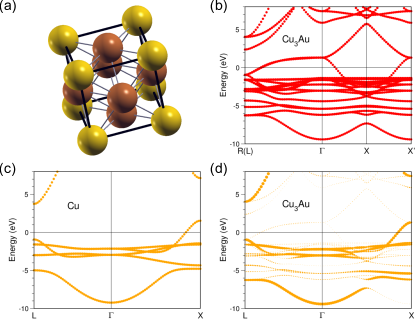
This correspondence is a general issue and can provide insights into the the underlying physics. An early applicationDavenport et al. (1988) of band unfolding was motivated by the observation that the photoemission of simple cubic Cu3Au closely resembles that of fcc Cu: the calculated bands of Cu3Au, Fig. 1(b), show significantly more bands with dispersions different that of Cu, Fig. 1(c). However, applying a -projection technique to the Cu3Au bands — treating the Cu3Au structure as an ordered supercell impurity phase, Fig. 1 — not only recovers the fcc-like band structure, but also reveals which “Cu” states hybridize and their relative weights, going beyond simply “unfolding” the bulk bands. Thus, -projection can provide key insights to the underlying physics.
A number of strategies have been developed to unfold the electronic bands from supercell calculations, often based on plane-wave methods or tight-binding methods.Davenport et al. (1988); Qi et al. (2010); Boykin and Klimeck (2005); Ku et al. (2010); Lee et al. (2013); Huang et al. (2014); Tomić et al. (2014); Tan et al. (2016) In principle, the procedure is straightforward, especially for plane wave-based methods, but can become time-consuming if done naively, especially in cases such as separating overlayer and substrate contributions. In this paper we present details of an efficient layer -projection method that allows us to study the local band structure,Qi et al. (2010); Chen and Weinert (2014) and the relationship to angle-resolved photoemission spectroscopy (ARPES)Chen et al. (2016a, 2017) and scanning tunneling microscopy/spectroscopy (STM/STS)Zhang et al. (2018) experiments.
The paper is organized as follows. In Section II, we discuss the -projection band unfolding technique and computational details of density-functional theory (DFT) calculations. In Section III, we present applications of the method to four interface structures: graphene bilayer (gr-2L) on H-saturated SiC(0001), BAs monolayers on the ferromagnetic semiconductor CrI3 monolayer, silicene on Ag(111), and the bulk-surface decomposition of the Dirac state on the topological insulator Bi2Se3.
II METHOD AND COMPUTATIONAL DETAILS
In a system with translational symmetry defined by the set (of order ) translation operators , the irreducible representations (irreps) can be labeled by within the first Brillouin zone. (The set of translations are integral multiples of the direct lattice vectors , while reciprocal lattice vectors as well as are given in terms of .) The character of the for the irrep is . Applied to a function , the projection operator
| (1) |
will project out that part that transforms as the th irrep
| (2) |
and . Since , any function can be decomposed into pieces that transform as the irreps labeled by
| (3) |
and measures the relative weight of this to . Note that this is general, and the function itself need not actually possess any translational symmetry, thus allowing this -projection to be applied even to single impurity (GF) calculations where the translational symmetry is explicitly lost. Since the irreps labeled by and + are the same, the projection operator puts into the form
| (4) |
where is related to the standard Fourier transform , ,
| (5) |
This connection to the Fourier coefficients provides a prescription for making the -projected decomposition. When the system possess, at least approximately, the translational symmetry defined by the , the Fourier coefficients will have peaks at the corresponding values; when this is not the case, i.e., the projection is done on the “wrong” translational symmetry, the weights will be spread throughout -space.
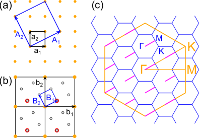
In practice, calculations are often done in a supercell geometry relative to a primitive cell (c.f., Fig. 2) with direct lattice vectors and reciprocal lattice basis vectors , , where are integers. In this case, because the translational symmetries are commensurate, the Fourier coefficients, Eq. (5), are non-zero at only specific values. A state calculated at will (possibly) have non-zero Fourier coefficients for , but may not be a reciprocal lattice vector of the primitive cell:
where , are integers, , belongs to the primitive lattice, and is in the first BZ of the primitive cell ( is fractional), but is equal to a reciprocal lattice vector of the supercell. If the supercell is times as large as the primitive, then there will be distinct , and hence a function calculated at in the supercell can be decomposed (-projected) into pieces corresponding to of the primitive cell.
For an ideal supercell, this decomposition is exact since it is a simple consequence of translational symmetry and recovers the primitive band structure with or 0; for defect systems and interfaces, the norm will be between zero and one.
The above scheme requires determining and then the weight for in the “primitive” cell. For bulk defect systems, the spatial integration is over the whole space. For interface systems, or for modeling STM or other probes that measure local properties, the integration volume entering the weight calculation should be restricted.
Our implementation, which uses FFTs, provides an efficient approach and has been used in plane wave (pseudopotential and PAW) methods and augmented methods (FLAPW and LASTO), and also can be adapted to LCAO ones. The first step is to determine from the wave function calculated in the supercell at , . For plane wave-based methods, all the wave function coefficients not corresponding to and are simply zeroed out; for other basis sets (e.g., LCAO) or when the lattices are not commensurate, an initial step is to evaluate the wave function in real space on the FFT mesh, back transform to reciprocal space, and then zero out the appropriate coefficients.
The projected wave function at this point can be put back into the normal basis used to represent the wave function, but now with modified coefficients. Then the standard machinery used to calculate overlaps (e.g., local density of states) can be used to calculate the weight, restricting the integration to a particular region of space as necessary. This restriction corresponds to including a step function (non-zero only in the region of interest) in the calculation of the weight. For plane wave components (including augmented methods like the FLAPW), this convolution is easily done: (i) FFT to real space; (ii) square, ; (iii) back transform to reciprocal space to obtain the Fourier coefficients ; and finally (iv) performing the sum . Note that the maximum in the sum is simply twice the plane wave cutoff of the wave functions, and hence the sum is exact despite the fact that the step function has a slow () convergence. For layer regions of space, (with ), the Fourier coefficients of the step function are particularly simple
Our implementation is different from Ref. Tan et al., 2016 that directly uses a projector built from the Heaviside function () to seperate contributions of different layers.
Prior to the band unfolding, we carried out DFT calculations using the Vienna Ab Initio Simulation Package Kresse and Furthmüller (1996) for the proposed systems. The pseudopotentials were constructed by the projector augmented wave method.Blöchl (1994); Kresse and Joubert (1999) van der Waals dispersion forces between the adsorbate and the substrate were accounted for through the optPBE-vdW functional by using the vdW-DF method developed by Klimeš and Michaelides.Klimeš et al. (2010, 2011) The interface structure is modeled in terms of a repeated slab, separated from its periodic images by 10 Å vacuum regions. For gr-2L/SiC(0001), the slab is composed of a supercell of H-saturated SiC(0001) and a 22 supercell of the gr-2L. For BAs/CrI3, a 22 supercell of BAs on a 11 unit cell of CrI3 is used, and for silicene/Ag(111) a 33 supercell of silicene on 44 Ag(111) is chosen, resulting in a small lattice mismatch. To avoid artificial interactions between the polar slabs, two such slabs, oppositely oriented with mirror symmetry, are placed in each supercell for gr-2L/SiC(0001) and BAs/CrI3, while for silicene/Ag(111) the overlayers are symmetrically placed on both sides of the substrate. To sample the surface BZs a 1212 -centered Monkhorst-Pack -point mesh was used for gr-2L/SiC(0001), 1515 for BAs/CrI3, and 66 for silicene/Ag(111), respectively. Plane-wave energy cutoffs of 700 eV, 350 eV, 240 eV were used for the electronic structure calculations of the above three interfaces, respectively. The Bi2Se3 calculations were done using the Full-potential Linearized Augmented Plane Wave Weinert et al. (2009) method for 10 QLs in a single film geometry, i.e., no periodic images, and included spin-orbit. The plane wave cutoffs were 220 and 2000 eV for the wave functions and density/potential, respectively, and a 1212 -point mesh was used.
III APPLICATIONS TO INTERFACES
III.1 Effects of surface termination: graphene bilayer on 6H-SiC
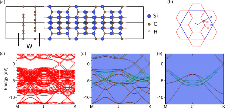
The 6H-SiC has two different (0001) surface terminations, either Si or C, and therefore, two different types of interface structures for bilayer graphene. Here we consider the situation where the two faces are saturated by H to model those experiments where H is used to passivate the interfaces between graphene layers and SiC(0001) surfaces;Riedl et al. (2009, 2010); Rajput et al. (2013) the case of graphene on the Si-face, including the role of the graphene buffer layer, has been treated earlier.Qi et al. (2010) Fig. 3(c) shows the calculated bands for gr-2L on the Si-face along the high symmetry lines extended into the second BZ of the supercell (c.f., Fig 3(b)). Because the graphene and substrate bands overlap, it is difficult to separate the various contributions. To focus on the graphene bands, we first do a layer projection, integrating over the region defined by W in Fig. 3(a). These bands, Fig. 3(d), while having removed the substrate, still do not simply resemble the free bilayer graphene. Along -M, the simple folding about MSC clearly visible, but this is not the case along -K, which corresponds to two high symmetry lines (–KSC and KSC–K) of the 22 supercell calculation. Finally doing the -projection to the 11 cell, Fig. 3(e), recovers bands that closely resemble the free-standing bilayer ones. Analysis of these bands provide insight into the interactions of the graphene and the substrate; for example, the mini-gaps are the result of the hybridization between the graphene and substrate.
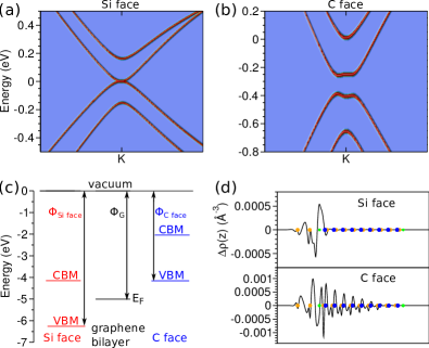
The -projected (unfolded) bands around the K point for gr-2L on the Si- and C-faces are shown in Figs. 4(a) and (b), respectively. On the H-passivated Si-terminated surface, Fig. 4(a), the interaction with the substrate has only a minor effect on these bands, opening a gap at K of less than about 10 meV, with the Fermi level located in the middle of the gap. On the C-face, Fig. 4(b), the induced gap is 0.13 eV, an order of magnitude larger than on the Si-face, and the graphene bilayer is n-doped with the Fermi level located at about 0.3 eV above the gap.
Using the picture proposed for heterostructures composed of silicene (germanene) monolayers and substrates, the perturbation on the bands of the overlayer about the Dirac point depends on the strength of the hybridization () and the energy differences () between the substrate states and the Dirac point.Chen et al. (2016b) A large and a small favor a strong perturbation to the Dirac states. Since gr-2L and the substrate interact mainly via vdW-type bonding, is expected to be rather small, which is supported by the observations that the overall -projected bands do not show large changes that could be attributed to strong bonding. Therefore, the difference in the band structure for gr-2L on different surfaces of SiC originates from the difference in between the two configurations determined by the band alignment of the two constituents. Fig. 4(c) depicts the band alignment of the free-standing gr-2L and SiC(0001). The Dirac point lies in the gap of the Si-face when their bands align, but lies below the valence band on the C-face. This alignment gives rise to a much larger when the gr-2L is placed on the Si-face than on the C-face ( is expected to be extremely small for the case of the C-face). Thus, the Fermi level can be expected to cross the Dirac point of the gr-2L on the Si-face and the states of the gr-2L near the Dirac point experience smaller perturbation. Figure 4(d) shows the planar-averaged charge density difference for gr-2L on the two different faces: The charge polarization in the graphene is much larger on the C-face than on the Si-face, indicating a stronger dipole field between the gr-2L and the C-face than the Si-face.
III.2 Magnetic proximity effect in BAs/CrI3
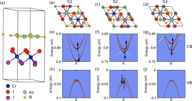
BAs was recently predicted to possess intriguing properties, i.e., a hexagonal structure with a direct gap of about 1.1 eV at the K point and a high mobility comparable to that of graphene. Xie et al. (2016) Generating spin-splittings in this system may be useful for designing spintronic devices in future applications. For such a purpose using magnetic semiconductors to induce spin splittings via the magnetic proximity effect has several advantages over doping magnetic atoms, such as preserving the atomic structure of the overlayer and making the manipulation easily controllable, as demonstrated in the successful realization of large spin-exchange splittings and anomalous Hall effect in graphene.Wei et al. (2016); Wang et al. (2015) Here we propose to generate spin-exchange splittings in BAs by making use of the magnetic proximity effect. A monolayer of the newly discovered ferromagnetic semiconductor CrI3 was used as the substrate. The lattice mismatch of a 22 supercell of BAs with CrI3 (experiment: 6.867 Å) is less than 2%, suggesting that vdW epitaxy could grow such heterostructures. We have examined three configurations for BAs/CrI3, obtained by shifting BAs along the [-110] direction, Fig. 5, referred to as S1, S2, S3, respectively. DFT calculations find that S3 has the lowest energy, about 9 meV per BAs unit cell lower than S1. Layer distances between the BAs and CrI3 monolayers are in the range of 3.80–3.95 Å. Unfolded band structures for BAs were obtained by projecting the supercell wave functions in BAs onto the -points of 11 BAs. The spin splittings are found to be configuration-dependent: negligibly small in the valence bands for S1 and S3, about 50 meV and 25 meV in the conduction bands for S1 and S3, respectively. The spin-splitting for S1 is comparable to the calculated value for graphene/EuO(111) (48 meV for the conduction band),Hallal et al. (2017) where the layer distance (2.57 Å) is much smaller than that for BAs/CrI3. Therefore, a large spin-exchange splitting can be effectively obtained in BAs via magnetic proximity effect in vdW heterostructures.
III.3 Interaction induced interface states: silicene on Ag(111)
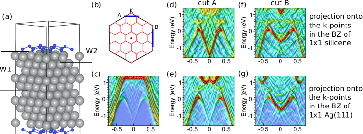
Silicene on Ag(111) has received much attention during the past few years. Unfortunately, the strong interaction between the overlayer and the substrate destroys the Dirac states in silicene. Chen and Weinert (2014); Guo et al. (2013); Wang and Cheng (2013); Cahangirov et al. (2013); Gori et al. (2013); Mahatha et al. (2014) However, recently an ARPES study observed that there are six pairs of half Dirac cones below the Fermi level on the edges of the first BZ of Ag(111), other than at the K points of 11 silicene.Feng et al. (2016) This observation led to the claim that Dirac cones exist in this system near the edge of the BZ, and were attributed to the interaction of the overlayer and the substrate. To clarify if Dirac states exist as claimed, we have performed DFT and layer -projection calculations to understand how the interaction between silicene and Ag(111) affects the electronic bands. The structural model is the one we used for our previous study, Chen and Weinert (2014) for which the simulated STM is in good agreement with the experiments.Feng et al. (2016); Vogt et al. (2012) Figure 6(b) shows the BZs of the 11 and 44 Ag(111), and cuts A and B are the high symmetry lines probed in the ARPES experiments and our -projection calculations.
Since previouslyChen and Weinert (2014) the linear dispersion observed for silicene/Ag(111) was found to originate from the substrate, we first consider the unfolded band structure along cut A for the substrate, Fig. 6(c), obtained by projecting the supercell wave functions in the spatial window W1 onto the -points in the BZ of 11 Ag(111). There are a few linear-like bands crossing the Fermi level, unlike the bands seen by the ARPES measurement (Fig. 3 in Ref. Feng et al., 2016).
Since ARPES is surface-sensitive, the experiments of Ref. Feng et al., 2016 using a photon energy of 21.218 eV for the ARPES experiments may have detected the surface bands of Silicene/Ag(111). According to Ref. Seah and Dench, 1979 the expected probing depth is 5 Åfor photons of 20-22 eV. Thus, we consider states with weight in W2 (silicene and the first Ag(111) layer) and -project them onto the BZs of 11 of silicene (Figs. 6(d,f)) and Ag(111) (Figs. 6(e,g)). For silicene an M-shaped band right below the Fermi level can be seen, but the V-shape part in the center has higher intensities than the two arms. For the substrate, the situation is opposite. Our results are also consistent with the previous study.Lian and Meng (2017) We further note that the calculated band structure agrees with the ARPES results (Fig. 3 in Ref. Feng et al., 2016) if one superimposes the unfolded band structures for both the silicene (Fig. 6(d)) and the substrate (Fig. 6(e)). Likewise, our calculations along cut B are also in good agreement with the ARPES experiments.Feng et al. (2016); Mahatha et al. (2014) However, as shown in Fig. 6, these are not Dirac states as claimed by the experiment. Nonetheless, our results are consistent with the ARPES experiment in that these bands are interface states resulting from the interaction between silicene and the substrate.
III.4 Bulk-surface decomposition of Dirac states in Bi2Se3
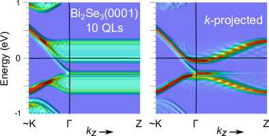
The topological surface states of Bi2Se3(0001) have been well studied, and calculations (and experiments) have shown that a minimum of about 5 QLs are necessary for the topological state to form a Dirac cone. For thinner films, there are still surface states, but are of the “normal” variety that can be understood as splitting off from the bulk bands. Since there is an evolution of the Dirac with thickness, there should be a connection between the models of standard and topological surface states. Here briefly analyze this connection. We consider 10 QLs of Bi2Se3. The calculated surface bands, Fig. 7 show the Dirac state, and a continuum of valence and conduction bands that result from the projection of the bulk bands. For the surface (or in a repeated slab) calculations, the translational symmetry perpendicular to the surface is broken, but the wave functions can still be labeled by ; in this case, if the calculations are converged and there are no artificial interactions between images, then there should be no variation in the calculations with . As seen in the left panel, this is indeed the case. -projecting these bands to the bulk cell (1 QL), =0 for K- and =0 for -Z, yields well-define bulk states, albeit the minigaps in the valence and conduction band along -Z reflecting the finite number of layers. The results show that the Dirac state is built up mainly of states with around split off from the valence band. This result shows that the standard arguments for normal surface state formation also hold for the topological surface states; for the topological states, the band inversion affects the character of the valence states out to about 0.2 of -Z, which in turn then contribute to the Dirac state; for fewer than 5 QLs, the surface state is seen to split off the conduction band, in which the minigaps are also larger because of the smaller number of layers.
IV CONCLUSIONS
In summary, we have presented a technique for unfolding electronic bands of materials, including an efficient scheme using FFTs to calculate the local -projected bands. This method allows us to effectively study the effects of interfaces by examining the spatial characteristics of the band structure, which is useful for understanding ARPES and STM/STS experiments. We applied the method to interfaces systems of gr-2L/SiC(0001), BAs/CrI3, silicene/Ag(111), and Bi2Se3/vaccuum. Our results revealed that the interactions of gr-2L and the two surfaces of SiC(0001) behave differently: The Si-face has minor effects on the band structure of the gr-2L, with a gap at the K point of only about 10 meV; on the C-face, however, a gap of about 130 meV at K is induced and gr-2L is -doped, caused by a strong electric dipole at the interface caused by a charge polarization. For the vdW heterostructure BAs/CrI3, we showed that the magnetic proximity effect can cause spin splittings of up to 50 meV in BAs that depend on the lateral registry of the two layers. For silicene/Ag(111), our results are consistent with recent ARPES experiments that find interface states whose dispersions on the edge of the first Brillouin zone of Ag(111) appear to be half Dirac cones, but demonstrate that they are not Dirac states. Finally, we have shown that the -projection can provide insight into the bulk origin of surface states, including the topological Dirac states.
Acknowledgements.
This work was supported by the National Natural Science Foundation of China (Grants No. 11774084) , and the U.S. National Science Foundation, EFMA-1741673.References
- Bednorz and Müller (1986) J. G. Bednorz and K. A. Müller, Z. Physik B - Condensed Matter 64, 189 (1986).
- Gupta et al. (2013) S. Gupta, B. Magyariköpe, Y. Nishi, and K. C. Saraswat, Journal of Applied Physics 113, 2234 (2013).
- Yu et al. (2010) R. Yu, W. Zhang, H.-J. Zhang, S.-C. Zhang, X. Dai, and Z. Fang, Science 329, 61 (2010).
- Chang et al. (2013) C. Z. Chang, J. Zhang, X. Feng, J. Shen, Z. Zhang, M. Guo, K. Li, Y. Ou, P. Wei, and L. L. Wang, Science 340, 167 (2013).
- Yang et al. (2013) H. X. Yang, A. Hallal, D. Terrade, X. Waintal, S. Roche, and M. Chshiev, Phys. Rev. Lett. 110, 046603 (2013).
- Wei et al. (2016) P. Wei, S. Lee, F. Lemaitre, L. Pinel, D. Cutaia, W. Cha, F. Katmis, Y. Zhu, D. Heiman, and J. Hone, Nature Materials 15, 711 (2016).
- Qi et al. (2015) J. Qi, X. Li, Q. Niu, and J. Feng, Phys. Rev. B 92, 121403 (2015).
- Zhang et al. (2016) Q. Zhang, S. A. Yang, W. Mi, Y. Cheng, and U. Schwingenschlögl, Advanced Materials 28, 7043 (2016).
- Qiao et al. (2014) Z. Qiao, W. Ren, H. Chen, L. Bellaiche, Z. Zhang, A. H. MacDonald, and Q. Niu, Phys. Rev. Lett. 112, 116404 (2014).
- Wang et al. (2015) Z. Wang, C. Tang, R. Sachs, Y. Barlas, and J. Shi, Phys. Rev. Lett. 114, 016603 (2015).
- Zhang et al. (2015) J. Zhang, B. Zhao, Y. Yao, and Z. Yang, Sci Rep 5, 10629 (2015).
- Novoselov et al. (2016) K. S. Novoselov, A. Mishchenko, A. Carvalho, and A. H. Castro Neto, Science 353, aac9439 (2016).
- Nordheim (1931) L. Nordheim, Annalen der Physik 401, 607 (1931).
- Gyorffy (1972) B. L. Gyorffy, Phys. Rev. B 5, 2382 (1972).
- Braspenning et al. (1984) P. J. Braspenning, R. Zeller, A. Lodder, and P. H. Dederichs, Phys. Rev. B 29, 703 (1984).
- Drittler et al. (1989) B. Drittler, M. Weinert, R. Zeller, and P. H. Dederichs, Phys. Rev. B 39, 930 (1989).
- Davenport et al. (1988) J. W. Davenport, R. E. Watson, and M. Weinert, Phys. Rev. B 37, 9985 (1988).
- Qi et al. (2010) Y. Qi, S. H. Rhim, G. F. Sun, M. Weinert, and L. Li, Phys. Rev. Lett. 105, 085502 (2010).
- Boykin and Klimeck (2005) T. B. Boykin and G. Klimeck, Phys. Rev. B 71, 115215 (2005).
- Ku et al. (2010) W. Ku, T. Berlijn, and C.-C. Lee, Phys. Rev. Lett. 104, 216401 (2010).
- Lee et al. (2013) C. C. Lee, Y. Yamada-Takamura, and T. Ozaki, Journal of Physics Condensed Matter 25, 345501 (2013).
- Huang et al. (2014) H. Huang, F. Zheng, P. Zhang, J. Wu, B.-L. Gu, and W. Duan, New Journal of Physics 16, 033034 (2014).
- Tomić et al. (2014) M. Tomić, H. O. Jeschke, and R. Valentí, Phys. Rev. B 90, 195121 (2014).
- Tan et al. (2016) Y. Tan, F. W. Chen, and A. W. Ghosh, Applied Physics Letters 109, 101601 (2016).
- Chen and Weinert (2014) M. X. Chen and M. Weinert, Nano Letters 14, 5189 (2014).
- Chen et al. (2016a) M. X. Chen, Z. Ge, Y. Y. Li, D. F. Agterberg, L. Li, and M. Weinert, Phys. Rev. B 94, 245139 (2016a).
- Chen et al. (2017) M. X. Chen, W. Chen, Z. Zhang, and M. Weinert, Phys. Rev. B 96, 245111 (2017).
- Zhang et al. (2018) W. Zhang, M. Chen, J. Dai, X. Wang, Z. Zhong, S. W. Cheong, and W. Wu, Nano Letters 18 (2018).
- Kresse and Furthmüller (1996) G. Kresse and J. Furthmüller, Phys. Rev. B 54, 11169 (1996).
- Blöchl (1994) P. E. Blöchl, Phys. Rev. B 50, 17953 (1994).
- Kresse and Joubert (1999) G. Kresse and D. Joubert, Phys. Rev. B 59, 1758 (1999).
- Klimeš et al. (2010) J. Klimeš, D. R. Bowler, and A. Michaelides, J. Phys.: Condens. Matter 22, 022201 (2010).
- Klimeš et al. (2011) J. Klimeš, D. R. Bowler, and A. Michaelides, Phys. Rev. B 83, 195131 (2011).
- Weinert et al. (2009) M. Weinert, G. Schneider, R. Podloucky, and J. Redinger, Journal of Physics: Condensed Matter 21, 084201 (2009).
- Riedl et al. (2009) C. Riedl, C. Coletti, T. Iwasaki, A. A. Zakharov, and U. Starke, Phys. Rev. Lett. 103, 246804 (2009).
- Riedl et al. (2010) C. Riedl, C. Coletti, and U. Starke, Journal of Physics D Applied Physics 43, 221–229 (2010).
- Rajput et al. (2013) S. Rajput, M. X. Chen, Y. Liu, Y. Y. Li, M. Weinert, and L. Li, Nature Communications 4, 2752 (2013).
- Chen et al. (2016b) M. X. Chen, Z. Zhong, and M. Weinert, Phys. Rev. B 94, 075409 (2016b).
- Xie et al. (2016) M. Xie, S. Zhang, B. Cai, Z. Zhu, Y. Zou, and H. Zeng, Nanoscale 8 (2016).
- Hallal et al. (2017) A. Hallal, F. Ibrahim, H. Yang, S. Roche, and M. Chshiev, 2d Materials 4, 025074 (2017).
- Guo et al. (2013) Z.-X. Guo, S. Furuya, J.-i. Iwata, and A. Oshiyama, Phys. Rev. B 87, 235435 (2013).
- Wang and Cheng (2013) Y.-P. Wang and H.-P. Cheng, Phys. Rev. B 87, 245430 (2013).
- Cahangirov et al. (2013) S. Cahangirov, M. Audiffred, P. Tang, A. Iacomino, W. Duan, G. Merino, and A. Rubio, Phys. Rev. B 88, 035432 (2013).
- Gori et al. (2013) P. Gori, O. Pulci, F. Ronci, S. Colonna, and F. Bechstedt, Journal of Applied Physics 114, 113710 (2013).
- Mahatha et al. (2014) S. K. Mahatha, P. Moras, V. Bellini, P. M. Sheverdyaeva, C. Struzzi, L. Petaccia, and C. Carbone, Phys. Rev. B 89, 201416 (2014).
- Feng et al. (2016) Y. Feng, D. Liu, B. Feng, X. Liu, L. Zhao, Z. Xie, Y. Liu, A. Liang, C. Hu, and Y. Hu, PNAS 113, 14656 (2016).
- Vogt et al. (2012) P. Vogt, P. De Padova, C. Quaresima, J. Avila, E. Frantzeskakis, M. C. Asensio, A. Resta, B. Ealet, and G. Le Lay, Phys. Rev. Lett. 108, 155501 (2012).
- Seah and Dench (1979) M. P. Seah and W. A. Dench, Surface and Interface Analysis 1, 2 (1979).
- Lian and Meng (2017) C. Lian and S. Meng, Phys. Rev. B 95, 245409 (2017).