Configuration-Sensitive Transport on Domain Walls of a Magnetic Topological Insulator
Yan-Feng Zhou
International Center for Quantum Materials, School of Physics, Peking University, Beijing 100871, China
Collaborative Innovation Center of Quantum Matter, Beijing 100871, China
Zhe Hou
International Center for Quantum Materials, School of Physics, Peking University, Beijing 100871, China
Collaborative Innovation Center of Quantum Matter, Beijing 100871, China
Qing-Feng Sun
sunqf@pku.edu.cnInternational Center for Quantum Materials, School of Physics, Peking University, Beijing 100871, China
Collaborative Innovation Center of Quantum Matter, Beijing 100871, China
CAS Center for Excellence in Topological Quantum Computation, University of Chinese Academy of Sciences, Beijing 100190, China
Abstract
We study the transport on the domain wall (DW) in a magnetic topological insulator.
The low-energy behaviors of the magnetic topological insulator are dominated
by the chiral edge states (CESs).
Here, we find that the spectrum and transport of the CESs at the DW are strongly
dependent on the DW configuration.
For a Bloch wall, two co-propagating CESs at the DW are doubly degenerate
and the incoming electron is totally reflected.
However, for a Néel wall, the two CESs are split
and the transmission is determined by the interference between the CESs.
Moreover, the effective Hamiltonian for the CESs indicates that
the component of magnetization perpendicular to the wall leads to the distinct transport behavior. These findings may pave a way to realize the low-power-dissipation spintronics
devices based on magnetic DWs.
Introduction.
The discovery of topological insulator (TI) has attracted intensive interest
in searching for topologically non-trivial states of condensed matter and subsequently,
triggered a series of occurrences of novel physical effectsHMZ ; Qxl .
The quantum anomalous Hall effect (QAHE), i.e.,
quantum Hall effect without the external magnetic field,
can be achieved in magnetic TI by introducing ferromagnetism in TI.LiuCX ; YuR
The magnetic TI has an insulating bulk classified by a Chern number
and conducting chiral edge states (CESs) through bulk-boundary correspondence.
In recent, QAHE has been
experimentally realized in Cr-dopedChangCZ1 ; Checkelsky ; Kou ; Bestwick ; Kandala and V-dopedChangCZ2 magnetic TI thin films,
and the Hall resistance shows a quantized value
implying that the Chern number of the
magnetic TIs which can be controlled by the magnetization directionLiuCX2 .
The boundary between magnetic TI domains of opposite magnetization
with forms a magnetic domain wall (DW) with
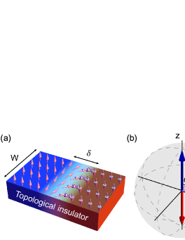
a magnetization rotation to minimize the total magnetic energy as shown in Fig.1(a).
Both the optimized configuration and thickness of the DW are determined by a balance
between competing energy contributionsbook1 ; book2 .
Two energetically favorable configurations are Bloch wall and Néel wall,
and the DW configuration can be controlled by Dzyaloshinskii-Moriya interactionThiaville ; ChenG1 ; ChenG2 ; DeJong .
Moreover, due to the different chirality of CESs across the DW, two
co-propagating CESs are expected to reside on the DW.
Very recently, the DWs of magnetic TI have been realized in Cr-doped
by the tip of a magnetic force microscopeYasudaK
and by spatially modulating the external magnetic
field using Meissner repulsion from a bulk superconductorRosen ,
and the chiral transport of CESs has been observed in these experiments.
Owing to the robustness of the CESs against backscattering, the DWs of magnetic TI have potential applications in the low-power-consumption spintronic devices, such as the nonvolatile racetrack memoryParkin .
Figure 1:
(a) Schematic diagram of a magnetic DW between two magnetic TI domains.
The direction of magnetization vector rotates continuously
from to direction inside the DW.
(b) The sphere of possible with the magnetization configurations corresponding to the different rotation modes defined by the azimuthal angle .
Here and corresponds to Néel wall and Bloch wall, respectively.
In this Letter, we study the transport of a two-terminal device
containing a DW of thickness and width in a magnetic TI [see Fig.1(a)].
In the low energy case, the transport behaviors of the magnetic TI are dominated
by CESs at the device edges as well as at the DW.
We calculate the band structure of magnetic TI with both Bloch wall and Néel wall.
For Bloch wall, two co-propagating linear CESs at the DW are doubly degenerate,
while for Néel wall a split is present.
As a result, the transport property is strongly dependent on the DW configuration.
In the Bloch wall case, the incoming electron with zero energy is totally reflected
regardless of the system parameters.
However, in the Néel case, the device functions as a chirality-based
Mach-Zehnder interferometry, so that
the transmission coefficient oscillates between zero and unity with changes in system parameters.
By constructing the scattering matrix of the device from the effective Hamiltonian,
these transport behaviors can be well understood.
Model.
As shown in Fig.1(a), two magnetic TI domains with upwards (blue region)
and downwards (red region) magnetization are separated by a DW.
The magnetization vectors are homogeneous away from the DW and change
continuously from direction to direction inside the DW.
The configuration of the DW can be described by magnetization vector
,
with a constant magnitude .
The azimuthal angle is a function of with
and the azimuthal angle defines the type of the magnetic DW.
From the sphere of possible magnetization vectors, the magnetic vector
in Néel wall and in Bloch wall [see Fig.1(b)].
The low-energy states of magnetic TI can be described by the HamiltonianYuR ; WangJ1 with
(1)
where the momentum and
being a four component electron operator,
where and label electrons from the top and bottom layers,
and and denote electrons with spin up and down, respectively.
and are Pauli matrices for spin and layer.
describes the coupling between the top and bottom layer.
In the calculation, we set the Fermi velocity ,
, , and .WangJ2
As , the magnetic TIs with Chern number are realized in the domains
with homogeneous upwards and downwards magnetization.
For the numerical calculation, we discretize the Hamiltonian Eq.(1) into a lattice version with a lattice constant .SDatta ; ChenCZ1 ; ChenCZ2 ; LiYH
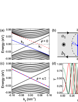
Figure 2:
(a) and (c) The band structure of an infinite slab of magnetic TI extending along the
direction with a Néel wall () in (a) and Bloch wall () in (c).
The width of the slab is and the thickness of the DW is .
The blue solid and red dashed lines represent the chiral modes on the DW.
(b) Schematic depicting the transport process based on the chiral modes.
(d) The zero-energy transmission coefficient of the device in Fig.1(a) versus
for several DW thickness with the width .
Chiral modes on the DW.
To study the spectrum of the CESs, we first consider an infinite slab of magnetic TI
containing a DW [see Fig.1(a)] which extends along the direction
and has a finite width in direction.
As the slab is invariant by translating along the axis,
the momentum is a good quantum number.
Figures 2(a) and 2(c) show the band structure of the slab
with a Néel wall () and Bloch wall (), respectively.
Inside the bulk gap, there are four linear chiral modes with
two co-propagating modes along the DW (blue solid and red dashed lines)
and two degenerate modes along the slab edges propagating in opposite direction
(black solid lines).
The presence of two chiral modes residing on the DW arises from the change
in Chern number from +1 to -1 across the DW.
For Bloch wall, the co-propagating modes on the DW are degenerate,
while for Néel wall, the chiral modes are split with energy
dispersions .
As the DW is located inside the slab, it has no effects on the chiral modes
on the edges as shown in Fig.2(a) and (c).
Let us construct the one-dimensional effective Hamiltonian for the co-propagating chiral modes on the DW to make the split clear. By a unitary transformation
in terms of new basis with
and
, and . are Pauli matrices.
Inside the DW with magnetization vector ,
both and are nontrivial due to the sign change of across the DW,
so that there exist two chiral statesQiXL2 ; ZhangRX .
As are coupled by element in Eq.(3),
to find the solutions of chiral states, we replace
and decompose the Hamiltonian as ,
in which contains the decoupled and consists of the element .
We solve first and treat as a perturbationSShen ; WangJ3 .
First, we solve the eigenequation for and .
It can be checked that and satisfy the anticommutation relation
.
Thus, the zero-energy eigenstate is the simultaneous eigenstate of and .
Consider the ansatz , where , , we have
(5)
With a substitution ,Flugge we arrive at the hypergeometric form of Eq.(5) and find the solution with
(see Supp for details)
Similarly, we find the solution of ,
with .
Here is normalization factor and is the hypergeometric function.
Written in a four-component notation, and .
Next, we consider the perturbation term by projecting the Hamiltonian onto the two zero-energy states leading to the one-dimensional effective HamiltonianSShen ; WangJ3 ,
(6)
It can easily be obtained that
and the nondiagonal element depends on the type of the DW.
For Néel wall, the magnetization vector , so
with the unit matrix . The effective Hamiltonian becomes
(7)
where
is the hybridization of the two states.
The excitation spectrum is .
These two modes are the nondegenerate chiral modes with a splitting
in [blue solid and red dashed lines in the Fig.2(a)].
However, for Bloch wall, , so and . The effective Hamiltonian becomes
(8)
The excitation spectrum is doubly degenerate with in accordance with Fig. 2(c). At this point, it can be seen that the split between the co-propagating chiral modes results from the component of the magnetization inside the DW and depends
on the type and thickness of the DW.
Transport on the DW.
To study the effect of DW configuration on the transport of the DW of magnetic TI,
we construct a two-terminal device [see Fig.1(a)] which contains a DW in the center region
and two semi-infinite left and right magnetic TI domains.
For low incident energy, the transport occurs via the CESs and
Fig.2(b) depicts the transport process.
By using the
nonequilibrium Green’s function method, the transmission coefficients can be
obtained fromSDatta ; sun1 ; sun2 ; sun4 ,
with the incident energy , retarded/advanced Green’s function , and
line-width function .
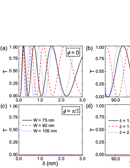
Figure 3: (a) and (c) The transmission coefficient versus DW thickness for
(a) Néel wall () and for (c) Bloch wall () in several widths for . (b) and (d) versus width for (b) Néel wall and (d) Bloch wall in several DW thicknesses for .
When an electron propagating along the mode (black arrow from
the left terminal) arrives at the trijunction ,
it is scattered into the chiral modes and in the DW region as shown in Fig.2(b).
After the propagation along the DW, the electron is scattered
off the trijunction and gets into the outgoing modes and eventually.
Fig.2(d) shows the transmission coefficient at
as a function of which specifies the type of the DW.
is the periodic function of with the period ,
so we only show the results for .
It can be observed in Fig.2(d) that for Bloch wall (),
the transmission coefficient and remains unchanged with the change
in the DW thickness .
However, deviating from , oscillates between 0 and 1 with the change
in and DW thickness , and is symmetric about ,
i.e. .
These results suggest that the current of the device in Fig.1(a)
can be switched on or off by changing the magnetization configuration of the DW.
Such a switch effect has an underlying application in spintronics, because that
the current is completely layer-locked spin-polarizedZhangRX ; WuJ .
Let us study the Néel wall and Bloch wall in detail.
Fig.3 shows the dependence of transmission coefficient
on the DW thickness and device width .
For Néel wall, approaches zero as the thickness of the DW vanishes [see Fig.3(a)].
With increasing in the thickness of the DW, oscillates between 0 and 1 for a fixed width .
The thinner the DW is, the faster oscillates.
Moreover, shows a periodic function of the device width
and the period is small for thick DW [see Fig.3(b)].
These imply that the device with Néel wall exhibits the behavior of a two-path interferometer.
However, for Bloch wall, the transmission coefficient is vanishing regardless of
the system parameters [see Fig.3(c,d)].
At this point, we can see that the two different DWs show absolutely different transport behaviors.
Below, based on the effective Hamiltonian Eqs.(7 and 8), we construct the scattering matrix of the two-terminal device to understand the underlying physics.
To find the scattering matrix which relates the incoming modes to the outgoing modes,
we return to the Hamiltonian [see Eqs.(3 and 4)]
to see the origin of the chiral modes and in Fig.2(b).
For left magnetic TI domain with ,
, is nontrivial and is trivial.
So and at the edge can be obtained by solving the Hamiltonian
with open boundary conditions solely, which is similar with the mode .
On the other hand, for right magnetic TI domain with ,
is trivial and is nontrivial.
Similarly, and can be obtained from the Hamiltonian , which is similar with .
Considering that and ( and ) are the bound state solutions of the () and have the same chirality, at the trijunction [see Fig.2(b)],
the mode () is scattered onto () and at the trijunction ,
the mode () is scattered into ().
For Néel wall, the solutions of the chiral modes on the DW [see Fig.2(b)] can be found as
from the Hamiltonian in Eq.(7).
Thus, the scattering matrix of the trijunction , accounts for the scattering of the incoming modes onto .
Similarly, the scattering matrix describes the trijunction is ,
where the modes are scattered onto the outgoing modes .
The scattering amplitude of the two-terminal device is found by
composing the scattering matrices,
(9)
where the second matrix contains the contribution of the dynamical phase and is the momentum of modes .
In this case, the incoming electron from the chiral mode is equally split into
CESs and at , then converge at and are finally scattered onto the
outgoing modes , which serves as a Mach-Zehnder interferometry.Mach1 ; Mach2
From Eq.(9), the transmission coefficient is obtained as
with .
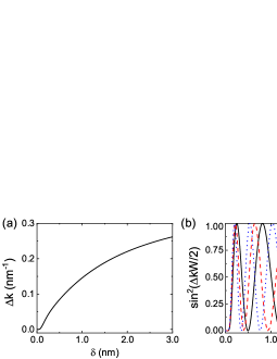
Fig.4 shows and as functions of the thickness of the DW. It can be seen that shows a good consistency with the of Fig.3(a)
and is a periodic function of the width of the device
in accordance with Fig.3(b).
Moreover, for a general DW defined by , the hybridization so that the coefficient is the same for , , and [see Fig.2(d)].
Figure 4: (a) Momentum difference between the modes as a function of the thickness of the DW for zero energy extracted from the band structure [see Fig.2(a)].
(b) versus the thickness for several width .
For Bloch wall, the co-propagating chiral modes on the wall are doubly degenerate
and which can be obtained from the Hamiltonian
in Eq.(8).
This means that the incoming mode () is totally reflected onto ().
This results a zero transmission coefficient which is consistent with Fig.3(c) and (d).
At this point, we have well understood the low-energy transport behavior of
the device containing a DW based on the effective Hamiltonian.
Conclusions.
In short, we find that the spectrum of the chiral modes is strongly dependent
on the detailed configuration of the DW.
For Bloch walls, the chiral modes are doubly degenerate,
while for Néel walls a split is present.
Correspondingly, the devices with different DW configuration show
very distinct transport behaviors.
In Bloch case, the current through the device vanishes regardless of system parameters.
However, in the Néel case, the transmission coefficient of the DW oscillates
between zero and unity with changes in system parameters and
is determined by the interference between the chiral modes.
From the scattering matrix of the device derived from the effective Hamiltonian of the chiral modes, these transport behaviors can be well understood.
These findings may pave a way to control the layer-locked spin-polarized current based on magnetic DWs.
Acknowledgments.
This work was financially supported by National Key R and D Program of China (2017YFA0303301),
NBRP of China (2015CB921102), and NSF-China (Grant No. 11574007).
References
(1)
M.Z. Hasan and C.L. Kane, Rev. Mod. Phys. 82, 3045 (2010).
(3)
C.-X. Liu, X.-L. Qi, X. Dai, Z. Fang, and S.-C. Zhang, Phys. Rev. Lett. 101, 146802 (2008).
(4)
R. Yu, W. Zhang, H.-J. Zhang, S.-C. Zhang, X. Dai, and Z. Fang, Science 329, 61 (2010).
(5)
C.-Z. Chang, J. Zhang, X. Feng, J. Shen, Z. Zhang, M. Guo,
K. Li, Y. Ou, P. Wei, L.-L. Wang, Z.-Q. Ji, Y. Feng, S. Ji,
X. Chen, J. Jia, X. Dai, Z. Fang, S.-C. Zhang, K. He, Y. Wang, L. Lu,
X.-C. Ma, Q.-K. Xue, Science 340, 167 (2013).
(6)
J.G. Checkelsky, R. Yoshimi, A. Tsukazaki, K.S. Takahashi, Y. Kozuka, J. Falson, M. Kawasaki,
and Y. Tokura, Nat. Phys. 10, 731 (2014).
(7)
X. Kou, S.-T. Guo, Y. Fan, L. Pan, M. Lang, Y. Jiang, Q. Shao, T. Nie,
K. Murata, J. Tang, Y. Wang, L. He, T.-K. Lee, W.-L. Lee, and K.L. Wang, Phys. Rev. Lett. 113, 137201 (2014).
(8)
A.J. Bestwick, E.J. Fox, X. Kou, L. Pan, K.L. Wang, and D. Goldhaber-Gordon, Phys. Rev. Lett. 114, 187201 (2015).
(9)
A. Kandala, A. Richardella, S. Kempinger, C.-X. Liu, and N. Samarth, Nature Commun. 6, 7434 (2015).
(10)
C.-Z. Chang, W. Zhao, D.Y. Kim, H. Zhang, B.A. Assaf, D. Heiman,
S.-C. Zhang, C. Liu, M.H.W. Chan, and J.S. Moodera, Nat. Mater. 14, 473 (2015).
(12)
A. Hubert and R. Schäfer, Magnetic Domains: The Analysis of Magnetic Microstructures
(Springer, Berlin, 1998).
(13)
N.A. Spaldin, Magnetic Materials: Fundamentals and Applications
(Cambridge University Press, Cambridge, 2014).
(14)
A. Thiaville, S. Rohart, É. Jué, V. Cros, and A. Fert, Europhys. Lett. 100 57002 (2012).
(15)
G. Chen, J. Zhu, A. Quesada, J. Li, A.T. N’Diaye, Y. Huo, T.P. Ma, Y. Chen, H.Y. Kwon, C. Won,
Z.Q. Qiu, A.K. Schmid, and Y.Z. Wu, Phys. Rev. Lett. 110, 177204 (2013).
(16)
G. Chen, T. Ma, A.T. N’Diaye, H. Kwon, C. Won, Y. Wu, and A.K. Schmid, Nature Commun. 4, 2671 (2013).
(17)
M.D. DeJong and K. L. Livesey, Phys. Rev. B 92, 214420 (2015).
(18)
K. Yasuda, M. Mogi, R. Yoshimi, A. Tsukazaki, K.S. Takahashi, M. Kawasaki, F. Kagawa, and Y. Tokura, Science 358, 1311 (2017).
(19)
I.T. Rosen, E.J. Fox, X. Kou, L. Pan, K.L. Wang, and D. Goldhaber-Gordon, npj Quantum Materials 2, 69 (2017).
(20)
S.S.P. Parkin, M. Hayashi, L. Thomas, Science 320, 190 (2008).
(21)
J. Wang, B. Lian, and S. C. Zhang, Phys. Rev. B 89, 085106 (2014).
(22)
J. Wang, Phys. Rev. B 94, 214502 (2016).
(23)
S. Datta, Electronic Transport in Mesoscopic System,
(Cambridge University Press, Cambridge, 1995).
(24)
C.-Z. Chen, J.J. He, D.-H. Xu, and K.T. Law, Phys. Rev. B 96, 041118 (2017).
(25)
C.-Z. Chen, Y.-M. Xie, J. Liu, P.A. Lee, and K.T. Law, Phys. Rev. B 97, 104504 (2018).
(26)
Y.-H. Li, J. Liu, H. Liu, H. Jiang, Q.-F. Sun, and X. C. Xie, arXiv:1804.10872 (2018).
(27)
X.-L. Qi, Y.-S. Wu, and S.-C. Zhang, Phys. Rev. B 74, 085308 (2006).
(28)
R.-X. Zhang, H.-C. Hsu, and C.-X. Liu, Phys. Rev. B 93, 235315 (2016).
(31)
S. Flügge, Practical Quantum Mechanics (Springer, Berlin, 1999).
(32)
See Supplementary Material for detailed calculations.
(33)
W. Long, Q.-F. Sun, and J. Wang, Phys. Rev. Lett. 101, 166806 (2008).
(34)
Q.-F. Sun and X.C. Xie, Phys. Rev. Lett. 104, 066805 (2010).
(35)
Y.-F. Zhou, Z. Hou, Y.-T. Zhang, and Q.-F. Sun, Phys. Rev. B 97, 115452 (2018).
(36)
J. Wu, J. Liu, and X.-J. Liu, Phys. Rev. Lett. 113, 136403 (2014).
(37)
R. Ilan, F. de Juan, and J.E. Moore, Phys. Rev. Lett. 115, 096802 (2015).
(38)
Y. Ji, Y. Chung, D. Sprinzak, M. Heiblum, D. Mahalu, and
H. Shtrikman, Nature 422, 415 (2003).
Supplemental Material for “Configuration-Sensitive Transport on Domain Walls of a Magnetic Topological Insulator”
Yan-Feng Zhou, Zhe Hou, and Qing-Feng Sun
I Analytical solution of the Hamiltonian
First, we solve the eigenequation for and ,
(10)
It can be checked that and satisfy the anticommutation relation .
Thus, the zero-energy eigenstate is the simultaneous eigenstate of and .
Consider the ansatz , where , , and , we have
(11)
In order to solve the differential equation, we use instead of the variable .Flugges With
we arrive at,
(12)
(13)
with , , and .
This equation has poles at and therefore leads to hypergeometric solutions.
Let’s set
(14)
with
(15)
(16)
we get
Then substituting these expressions into Eq.(13),
we arrive at the Gaussian equation
(17)
In the derivation of Eq.(17), we have used identity and .
Then Eq.(17) has the special solution
(18)
with the hypergeometric function and a normalized constant .
To determine the value of , we turn to the boundary conditions and .
For the limit or , .
We apply the transformation rules for passing over from the argument to of the hypergeometric function,
With and , this leads to
(20)
The boundary condition implies that and .
From Eq.(16), one can see that the condition is satisfied always.
From the condition and ,
can only take .
On the other hand, for the limit or , the solution (18) becomes or
The boundary condition implies that .
From Eq.(15), this condition is satisfied at .
Finally, we obtain the wavefunction of zero energy for ,
(21)
Next, we solve the eigenequation for and ,
(22)
In order to solve this differential equation, we use instead of the variable and considering the ansatz , the Eq.(22) becomes
(23)
which has the same form as Eq.(13). This allows us to reuse the previous results. To satisfy the boundary conditions and ,
we can obtain the wave function of zero energy for ,
(24)
with a normalized constant .
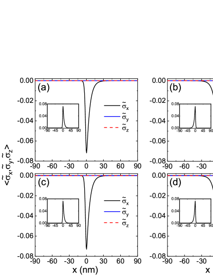
Figure S1 displays the distributions of the probability density and the expectation value of in the bound state compared with numerical calculation. Both states are distributed around the DW, and only is non-vanishing and negative which is consist with .
Moreover, the analytical results are well consistent with numerical results.
Figure 5: Distribution of expectation value of in the bound state at the DW solved from (a) and (b) with momentum by numerical calculation.
(c) and (d) are the analytic results from and in Eqs.(21) and (24).
The insets display probability density of the bound states.
References
(1)
S. Flügge, Practical Quantum Mechanics (Springer, Berlin, 1999).