Spin Structure of K Valleys in Single-Layer WS2 on Au(111)
Abstract
The spin structure of the valence and conduction bands at the and ’ valleys of single-layer WS2 on Au(111) is determined by spin- and angle-resolved photoemission and inverse photoemission. The bands confining the direct band gap of 1.98 eV are out-of-plane spin polarized with spin-dependent energy splittings of 417 meV in the valence band and 16 meV in the conduction band. The sequence of the spin-split bands is the same in the valence and in the conduction bands and opposite at the and the ’ high-symmetry points. The first observation explains "dark" excitons discussed in optical experiments, the latter points to coupled spin and valley physics in electron transport. The experimentally observed band dispersions are discussed along with band structure calculations for a freestanding single layer and for a single layer on Au(111).
pacs:
Since the discovery of graphene, two-dimensional materials have driven intense research effort due to their fascinating electronic and optical properties Wang et al. (2012). The option of stacking different two-dimensional materials on top of each other opens the way of tailoring specific material properties Lee et al. (2016). With respect to optoelectronic applications, semiconducting materials such as W- and Mo-based transition metal dichalcogenides (TMDCs) are especially appealing. These materials exhibit an indirect-to-direct band-gap transition upon reducing the thickness to a single layer (SL) Cheiwchanchamnangij and Lambrecht (2012); Jin et al. (2013); Cappelluti et al. (2013); Zhang et al. (2014a); Yeh et al. (2015). Since the SL material has no inversion symmetry, the Kramers degeneracy is lifted which causes spin-dependent band splittings due to spin-orbit interaction. The spin texture with alternating spin orientations at the and ’ high-symmetry points leads to coupled spin and valley physics and possible applications Di Xiao et al. (2012).
The valence bands of SL W- and Mo-based TMDCs have been studied in detail with photoemission techniques Klein et al. (2001); Zhang et al. (2014b); Maciej Dendzik et al. (2015); Miwa et al. (2015); Antonija Grubisic Cabo et al. (2015); Duy Le et al. (2015); Zhang et al. (2016); Bruix et al. (2016); Ulstrup et al. (2016a, a); Sung-Kwan Mo et al. (2016). The detection of two different excitons A and B in optical experiments Mak et al. (2010) is explained by the spin-dependent energy splitting of the valence band. So far, experimental information about the unoccupied conduction bands is limited to scanning tunneling spectroscopy Zhang et al. (2015); Bruix et al. (2016) and time-resolved photoemission data Antonija Grubisic Cabo et al. (2015); Ulstrup et al. (2016b, 2017a), yet without spin resolution. Since the conduction bands are also predicted to have a spin-dependent energy splitting Zhu et al. (2011); Kosmider et al. (2013); Liu et al. (2013); Kormányos et al. (2015), spin-allowed and spin-forbidden ("dark") transitions are expected. This leads to so-called dark excitons which possibly influence the efficiency of SL TMDC devices Ye et al. (2015); Echeverry et al. (2016).
In this Letter, we use a combined angle-resolved photoelectron spectroscopy (ARPES) and angle-resolved inverse-photoemission (IPE) setup, both with spin resolution, to investigate the spin texture of the highest valence bands and lowest conduction bands of SL WS2 grown on Au(111). We compare our experimental results with band structure calculations for the isolated SL and for a SL on Au(111).
The sample used in the present work was single orientation, SL WS2 on Au(111) with a coverage of about 45%. For spin-resolved experiments, a single orientation of the SL WS2 domains is essential because otherwise the measured spin polarization at the and ’ points would be reduced or even cancelled by mixed contributions from and ’. The SL WS2 was grown at the SuperESCA beam line of the Elettra synchrotron-radiation facility in Trieste by evaporating tungsten at a partial pressure of H2S onto the Au(111) substrate, the single orientation was verified by x-ray photoelectron diffraction (XPD) Bignardi et al. (2018). In Münster, the sample was annealed in ultrahigh vacuum to remove contaminants. The sample quality was checked with low-energy electron diffraction (LEED). The LEED pattern showed the expected moiré structure due to the lattice mismatch between WS2 and Au as well as the same threefold rotational symmetry as measured just after sample preparation.
In our experimental approach, we are able to measure the energy dispersion and spin dependence of valence and conduction bands in the same chamber on the same sample Budke et al. (2007a). ARPES measurements are performed with unpolarized light of a He discharge lamp (h eV). The illuminated area on the sample is in the millimeter range. The photoemitted electrons are detected by a simulated 50 mm hemispherical analyzer (SHA 50 by FOCUS GmbH), that is mounted on a goniometer for angle-resolved measurements. The energy resolution was about 150 meV. The spin polarization of the emitted electrons is detected via spin-polarized low-energy electron diffraction (SPLEED) Feder and Kirschner (1981); Yu et al. (2007). The detector has a Sherman function of Budke et al. (2007a). For spin-resolved IPE, we use a spin-polarized electron source, which provides an electron beam of 3 mm diameter with a spin polarization of Stolwijk et al. (2014) and a beam divergence of about Zumbülte et al. (2015). For non-normal electron incidence on the sample, our setup is sensitive to the out-of-plane spin component Stolwijk et al. (2014). Emitted photons of h eV are detected by a bandpass-type detector Budke et al. (2007b); Thiede et al. (2015, 2018). The overall energy resolution of the IPE experiment is about 350 meV Budke et al. (2007b). The parallel component of the electron wave vector k∥ is determined by the emission and incidence angles in ARPES and IPE, respectively. All spectra have been normalized to 100 Sherman function in ARPES and complete spin polarization of the incoming electrons in IPE Donath (1994). During the measurements, the sample was at room temperature.
We have calculated the electronic structure of a freestanding WS2 layer as well as a SL WS2 on a six-layer slab of Au(111) using density functional theory including spin-orbit coupling. The structural models and methods used for the calculations are described in detail in Ref. Dendzik et al. (2017).
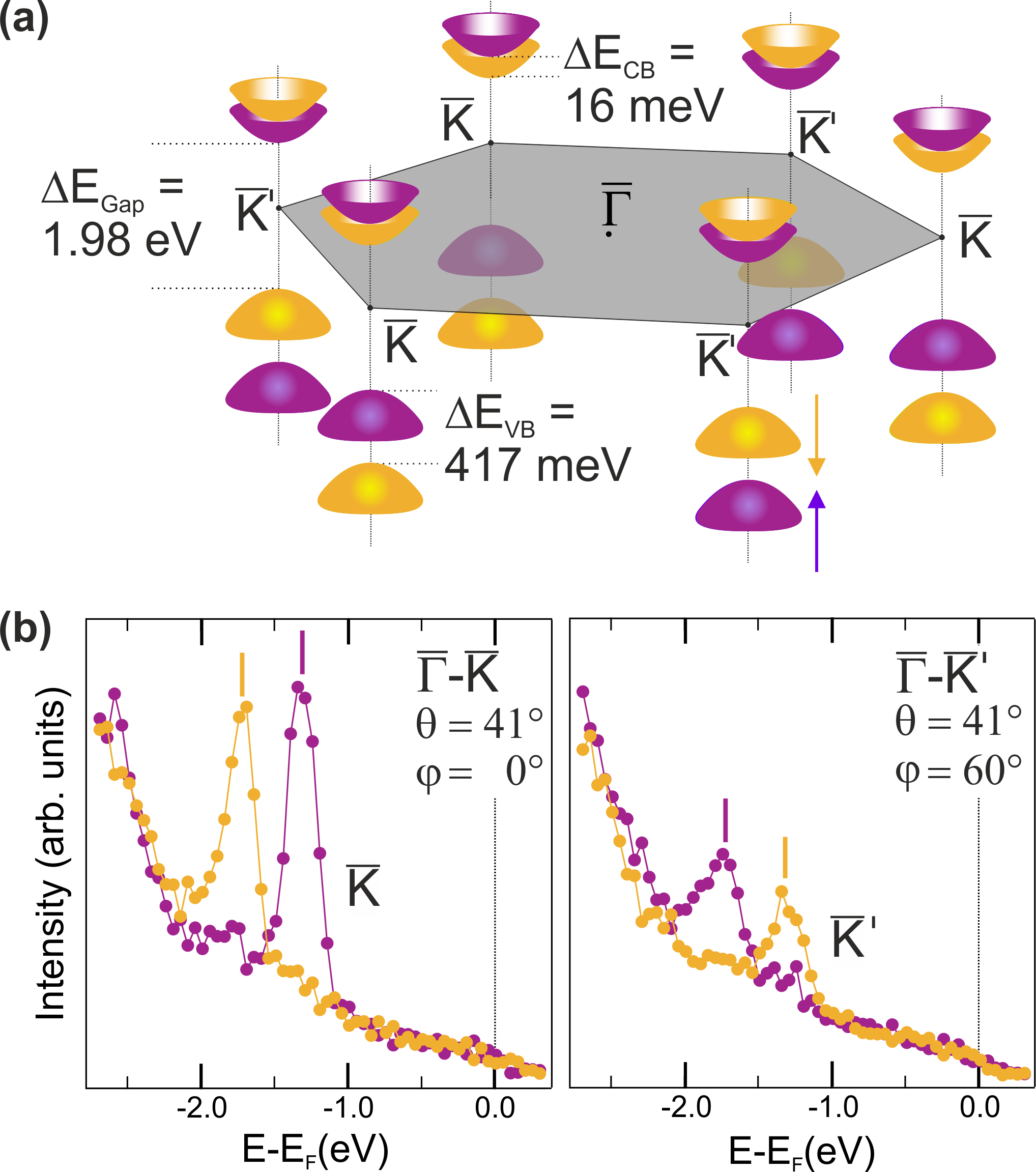
When studying the surface of bulk TMDC samples or SL films with multiple domain orientations, the experimental spin information is complicated by the signal of sublayers (spin-layer locking) Riley et al. (2014); Razzoli et al. (2017) or by mixed spin signals originating from and ’ Sung-Kwan Mo et al. (2016), respectively. So far, a spin-resolved ARPES study on single-oriented SL TMDC is only reported for MoS2 on Au(111), yielding out-of-plane spin-polarized valence bands with opposite sign at the and ’ points Bana et al. (2018). An equivalent spin texture in the valence band is expected for WS2 Zhu et al. (2011); Di Xiao et al. (2012); J Li et al. (2015); Tatsumi et al. (2016). Figure 1(b) shows our spin-resolved ARPES measurements for SL WS2/Au(111) at and ’. Purple and yellow dots denote data for electron spin polarization parallel or antiparallel to the surface normal, respectively. The valence band maximum (VBM) is found at E eV and eV for the two spin directions. Our results reveal a spin-dependent energy splitting of meV. This value is in good agreement with our calculation (431 meV) and other theoretical predictions Zhu et al. (2011); Ramasubramaniam (2012); Kosmider et al. (2013); Liu et al. (2013); Ye et al. (2014); Kormányos et al. (2015). The same size of the splitting was obtained in spin-integrated measurements for SL WS2 on different substrates Maciej Dendzik et al. (2015); Ulstrup et al. (2016a); Dendzik et al. (2017) as well as on bulk samples Latzke et al. (2015), while other references report slightly higher values Yuan et al. (2016); Forti et al. (2017).
Remarkably, the two oppositely spin-polarized valence band features (in the data for both and ’) show almost 100% spin polarization above background. Extrinsic spin-polarization effects caused by matrix-element effects based on orbital contributions as well as experimental parameters and geometry Donath (2018); Henk et al. (2018) can be ruled out by the following experimental finding obtained with unpolarized light: in the same experimental geometry with only the sample rotated azimuthally by , we obtain completely spin-polarized features at and ’, yet with reversed sign. These observations are only possible if two conditions are met: (i) the SL film has one single orientation, thus confirming the XPD results Bignardi et al. (2018), and (ii) the bands at the Brillouin-zone boundary are intrinsically spin polarized.
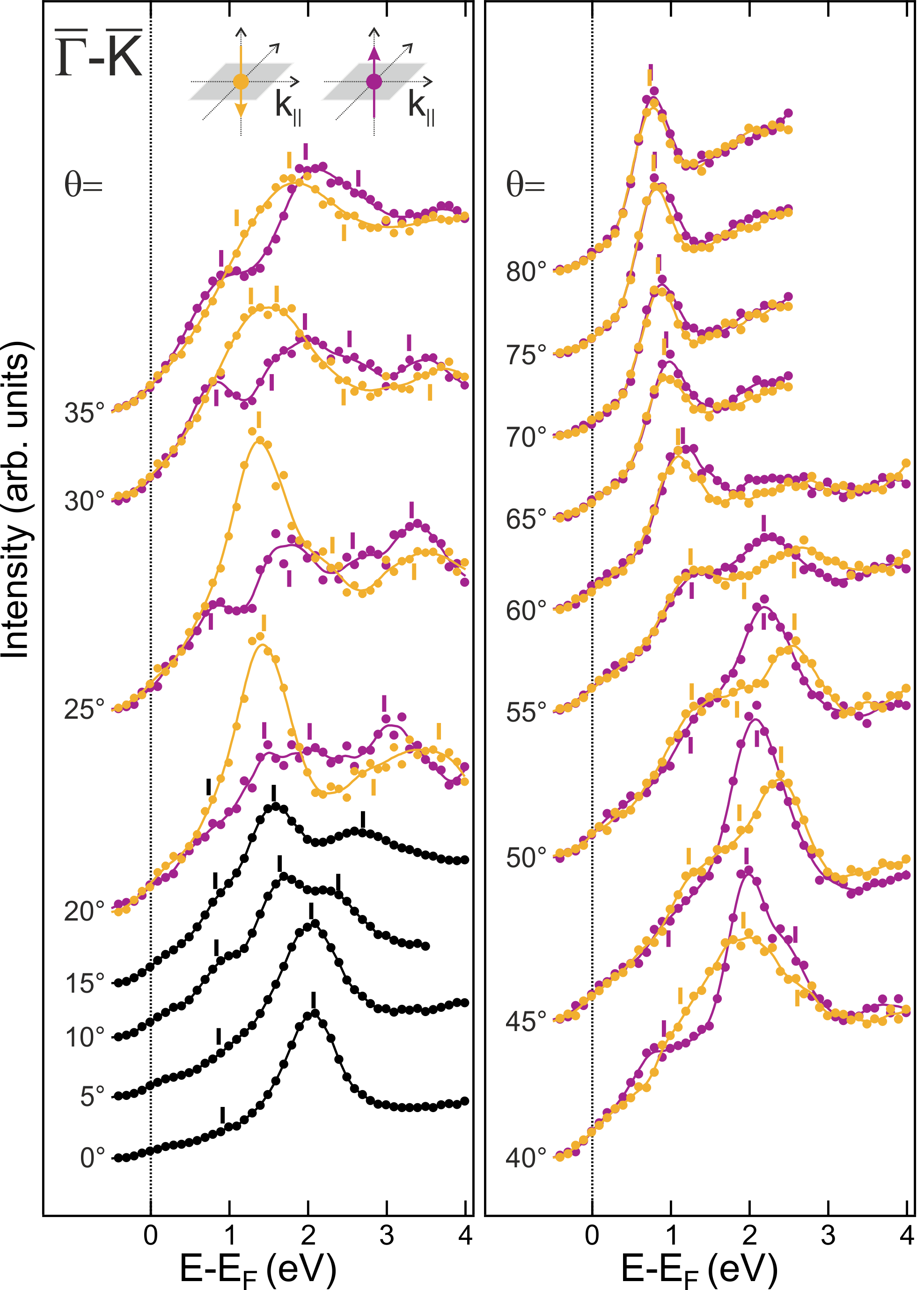
To get information about the size of the energy gap and the spin dependence of the confining bands, IPE measurements of the conduction bands are necessary. Figure 2 presents IPE spectra for various angles of electron incidence along -. As mentioned before, in our setup, out-of-plane sensitivity is only available for with increasing sensitivity for larger . Therefore, spin-integrated data are shown as black dots for . For , spin-resolved data for out-of-plane spin sensitivity are presented as purple (yellow) dots for spin polarization parallel (antiparallel) to the surface normal. Clear out-of-plane spin asymmetries in the conduction bands are detected. Estimated peak positions are marked by small vertical lines. The Fermi edge is visible in all ARPES (Fig. 1) as well as IPE spectra (Fig. 2). While WS2 sustains its semiconducting properties when deposited on Au(111) Dendzik et al. (2017), the uncovered metallic Au(111) areas cause the Fermi level onset in the spectra.
Our experimental results for the conduction bands are summarized in an plot in Fig. 3: Black, yellow, and purple squares denote peak positions in the spectra of Fig. 2 for spin-integrated, out-of-plane spin-down, and spin-up polarized data, respectively. The experimental data are presented along with calculations for (i) the projected bulk band structure of Au(111) [gray shaded area], (ii) a freestanding SL WS2 [gray lines], and (iii) a SL WS2 on top of a six layer slab Au(111) [blue dots]. The sizes of the blue dots are obtained from our supercell calculation and indicate the spectral weight of the effective band structure at each corresponding k point and energy interval resulting from the band unfolding method (for details, see Dendzik et al. (2017)). The theoretical results have been rigidly shifted in energy to match the experimental results of the lowest conduction band at . Notably, with this calibration, the bands at between 1.5 and 2.0 eV fit as well.
Bands in regions where Au(111) has no states, e.g. close to and below 1 eV close to , are expected to have almost pure WS2 character. Within the gray-shaded region Au bands exist, which might hybridize with WS2 bands. The experimental energy dispersions follow predominantly the band dispersions of the freestanding layer with some deviations where bands of Au and WS2 hybridize. The largest deviation between experiment and theory is observed for the lowest conduction band in the vicinity of , which appears in the experimental data with only low intensity. Remarkably, bands split off to lower energy around are also theoretically expected for the adsorbed layer compared with the freestanding layer (see Fig. 3), albeit not as much as experimentally observed.
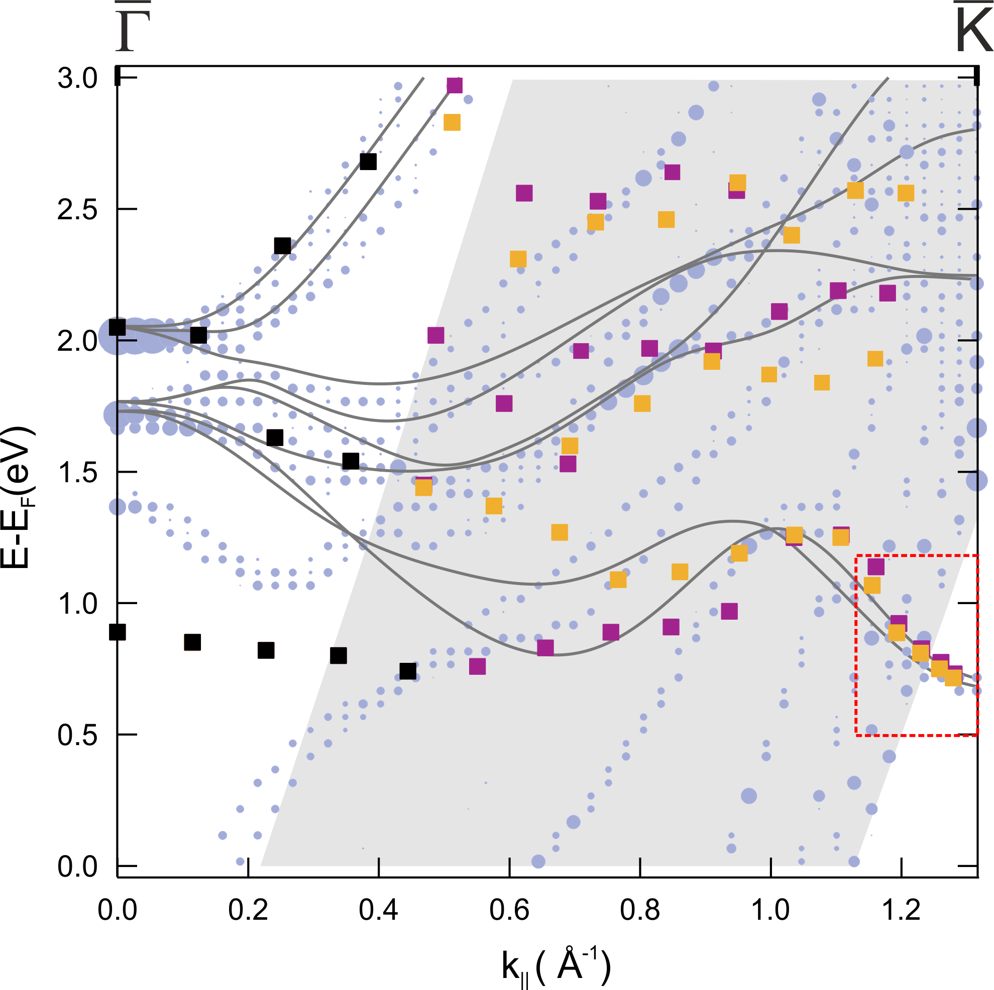
An important question about SL TMDCs is the position of the conduction band minimum (CBM). Most studies indicate the CBM to be at the point Klein et al. (2001); Mak et al. (2010); Splendiani et al. (2010); Kumar and Ahluwalia (2012); Zhao et al. (2013); Shi et al. (2013); Roldán et al. (2014); Sun et al. (2016). However, it is predicted that the energy at is only few milli-electron-volts lower than at the so-called Q point about halfway between and . There are even indications of the CBM being at the Q point Hsu et al. (2017). In our experiment, we find spectral features around Q, which are possibly influenced by Au states, with similar energies as the lowest spectral features at . Therefore, we cannot resolve whether the CBM position is at or at Q.
The key question with respect to the / valleys is the size of the energy gap and its spin structure. The lowest conduction band of WS2 at is found in a projected band gap of Au(111), and thus not influenced by Au states. Due to our photon energy of 9.9 eV, the accessible range is limited. Nevertheless, our data for come very close to at the given final-state energy (97 of -, see Fig. 3). Figure 4 shows close-ups of spin-resolved IPE data for = and = along - as well as data close to ’ ( = ) to check the sign reversal of the spin signal.
The peak positions for spin-up and spin-down differ only slightly. Since the two partial spin spectra are measured separately, spin splittings can be resolved that are much smaller than the energy resolution or the intrinsic linewidth of the spectral features. In the case of completely spin-polarized states, the spin splitting can be determined quantitatively even in the case of energetically overlapping states. Otherwise, the obtained value is at least a lower limit. Based on our results for the valence bands, we reasonably assume that the conduction bands are completely spin polarized as well.
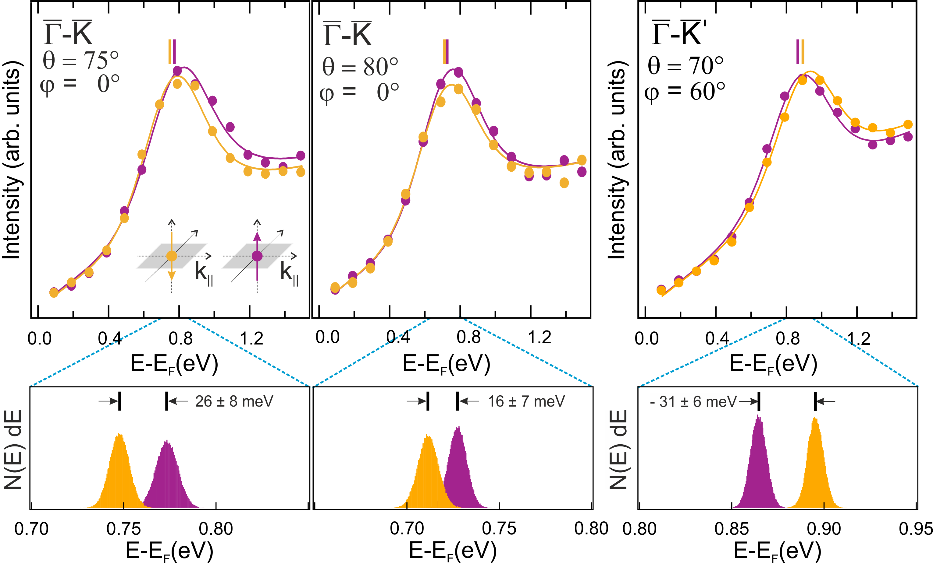
We determined the peak positions of spin-up and spin-down spectra separately by a least-squares fitting procedure (see the Supplemntal Material for details. The fit function is composed of a Lorentzian function, a linear background, and a step function at the position of the Lorentzian function to simulate the steplike background increase due to secondary processes Dose and Reusing (1980). The result is then multiplied by the Fermi function and convoluted with a Gaussian-shaped apparatus function Budke et al. (2007b); Stolwijk et al. (2014). To quantify spin splittings and illustrate the statistical uncertainties, we used an approach reported earlier Passek and Donath (1992); Donath and Ertl (1992). For each spectrum, we generated a series of 100,000 pseudoexperimental spectra by varying each measured data point according to its statistical uncertainty and fitted the peak positions of the spectra. We obtained a peak-position distribution for each measured spectrum and derived from these the spin splittings between respective partial spin spectra (examples are shown on an enlarged energy scale in the lower parts of 4). For , all spectra along - exhibit a spin splitting with the same sign (see Fig. 2). An important test is the measurement on the sample rotated azimuthally by : The data for along -’ also show a clear spin splitting, yet with reversed sign (see the right panel of Fig. 4)
The extracted spin splittings are a few tens of milli-electron-volts, decreasing to 31, 26 and 16 meV upon approaching the zone boundary for electron incidence angles of 70, 75, and 80∘, respectively. Our experimental value of 16 meV is slightly lower than calculated conduction band splittings. We obtained 29 meV in good agreement with other calculations (26 to 32 meV Zhu et al. (2011); Kosmider et al. (2013); Liu et al. (2013); Kormányos et al. (2015)).
The energy of the lowest conduction band in proximity to is determined to eV, which can be extrapolated to eV at by assuming a parabolic band behavior. Together with our result for the highest valence band, the size of the band gap amounts to eV. Quasiparticle calculations predict the band gap of freestanding SL WS2 in the range between 2.7 eV and 2.88 eV Ding et al. (2011); Ramasubramaniam (2012); Liang et al. (2013); Shi et al. (2013); Kormányos et al. (2015). Our determined band gap for WS2/Au(111) is significantly lower due to the enhanced screening of the Au substrate, as reported also for MoS2/Au(111) Bruix et al. (2016). Interestingly, a band gap of similar size (2.0 eV) was found for WS2/Ag(111) by time-resolved ARPES Ulstrup et al. (2017b).
An essential piece of information is the spin sequence of the valence and conduction bands. Our data for WS2 show that they are spin- split in the same way. In other words, the highest valence band is oppositely out-of-plane spin-polarized with respect to the lowest conduction band as sketched in Fig. 1 (a). Thus, the first spin-allowed (bright) transition is 16 meV higher in energy than the first dark transition.
Our experimental value for is important for theoretical studies, trying to determine the energy difference between dark and bright excitons Echeverry et al. (2016). Additionally, the electron-hole interaction within the exciton contributes to . A few studies report on "brightening" the spin-forbidden dark excitons in WSe2 Zhou et al. (2017); Zhang et al. (2017) and MoSe2 Jorge Quereda et al. (2018) by various methods. For SL WS2, a splitting between dark and bright excitons meV was reported from a photoluminescence experiment under the influence of an in-plane magnetic field M R Molas et al. (2017). While the lower energy of the dark exciton is consistent with our results, is much larger than . For SL WS2, the contribution of the electron-hole interaction is calculated to be in the order of 20 meV Echeverry et al. (2016) partially explaining the difference between and .
In conclusion, we studied the occupied and unoccupied electronic structure of SL WS2/Au(111) experimentally by spin-resolved direct and inverse photoemission and theoretically by calculations for the freestanding SL and a SL adsorbed on Au(111). The total energy gap amounts to eV, influenced by the screening of the Au substrate. Special attention was given to the spin structure of the VBM and the CBM at the /’ valleys. Based on our results, we provide a schematic band structure at the and ’ points, as it is sketched in Fig. 1(a). The highest valence band is found to be spin-split by meV, the lowest conduction band by meV. The sequence of the spin-split bands is the same below and above the Fermi level; i.e., the highest valence band is oppositely out-of-plane spin-polarized with respect to the lowest conduction band. As a consequence, the lowest direct transition is spin-forbidden, i.e., optically dark. The first bright transition, involving the second conduction band, is 16 meV higher in energy than the band gap. Our calculations show that the bands at the /’ valleys are almost unaffected by the Au substrate. Therefore, our results clarify important questions regarding band dispersion and spin structure for SL WS2 with its promising valleytronic properties for future optoelectronic applications.
We thank Marco Bianchi, Jürgen Henk, Marcel Holtmann, Peter Krüger, and Paolo Lacovig for helpful support. This work was supported by the Danish Council for Independent Research, Natural Sciences under the Sapere Aude program (Grant No. DFF-4002-00029) and by VILLUM FONDEN via the Center of Excellence for Dirac Materials (Grant No. 11744).
References
- Wang et al. (2012) Q. H. Wang, K. Kalantar-Zadeh, A. Kis, J. N. Coleman, and M. S. Strano, Nature Nanotechnol 7, 699 (2012).
- Lee et al. (2016) J. Y. Lee, J.-H. Shin, G.-H. Lee, and C.-H. Lee, Nanomaterials 6 (2016).
- Cheiwchanchamnangij and Lambrecht (2012) T. Cheiwchanchamnangij and W. R. L. Lambrecht, Phys. Rev. B 85, 205302 (2012).
- Jin et al. (2013) W. Jin, P.-C. Yeh, N. Zaki, D. Zhang, J. T. Sadowski, A. Al-Mahboob, A. M. van der Zande, D. A. Chenet, J. I. Dadap, I. P. Herman, P. Sutter, J. Hone, and R. M. Osgood, Phys. Rev. Lett. 111, 106801 (2013).
- Cappelluti et al. (2013) E. Cappelluti, R. Roldán, J. A. Silva-Guillén, P. Ordejón, and F. Guinea, Phys. Rev. B 88, 075409 (2013).
- Zhang et al. (2014a) X. Zhang, Q. Liu, J.-W. Luo, A. J. Freeman, and A. Zunger, Nat. Phys. 10, 387 (2014a).
- Yeh et al. (2015) P.-C. Yeh, W. Jin, N. Zaki, D. Zhang, J. T. Liou, J. T. Sadowski, A. Al-Mahboob, J. I. Dadap, I. P. Herman, P. Sutter, and R. M. Osgood, Phys. Rev. B 91, 041407 (2015).
- Di Xiao et al. (2012) Di Xiao, G.-B. Liu, W. Feng, X. Xu, and W. Yao, Phys. Rev. Lett. 108, 196802 (2012).
- Klein et al. (2001) A. Klein, S. Tiefenbacher, V. Eyert, C. Pettenkofer, and W. Jaegermann, Phys. Rev. B 64, 205416 (2001).
- Zhang et al. (2014b) Y. Zhang, T.-R. Chang, B. Zhou, Y.-T. Cui, H. Yan, Z. Liu, F. Schmitt, J. Lee, R. Moore, Y. Chen, H. Lin, H.-T. Jeng, S.-K. Mo, Z. Hussain, A. Bansil, and Z.-X. Shen, Nat. Nanotechnol. 9, 111 (2014b).
- Maciej Dendzik et al. (2015) Maciej Dendzik, Matteo Michiardi, Charlotte Sanders, Marco Bianchi, Jill A. Miwa, Signe S. Grønborg, Jeppe Vang Lauritsen, Albert Bruxi, Bjørk Hammer, and Philip Hofmann, Phys. Rev. B 92, 245442 (2015).
- Miwa et al. (2015) J. A. Miwa, S. Ulstrup, S. G. Sørensen, M. Dendzik, A. G. Čabo, M. Bianchi, J. V. Lauritsen, and P. Hofmann, Phys. Rev. Lett. 114, 046802 (2015).
- Antonija Grubisic Cabo et al. (2015) Antonija Grubisic Cabo, Jill A. Miwa, Signe S. Grønborg, Jonathon M. Riley, Jens C. Johannsen, Cephise Cacho, Oliver Alexander, Richard T. Chapman, Emma Springate, Marco Grioni, Jeppe V. Lauritsen, Phil D. C. King, Philip Hofmann, and Søren Ulstrup, Nano Lett. 15, 5883 (2015).
- Duy Le et al. (2015) Duy Le, Alexei Barinov, Edwin Preciado, Miguel Isarraraz, Iori Tanabe, Takashi Komesu, Conrad Troha, Ludwig Bartels, Talat S Rahman, and Peter A Dowben, J. Phys. Condens. Matter 27, 182201 (2015).
- Zhang et al. (2016) Y. Zhang, M. M. Ugeda, C. Jin, S.-F. Shi, A. J. Bradley, A. Martín-Recio, H. Ryu, J. Kim, S. Tang, Y. Kim, B. Zhou, C. Hwang, Y. Chen, F. Wang, M. F. Crommie, Z. Hussain, Z.-X. Shen, and S.-K. Mo, Nano Lett 16, 2485 (2016).
- Bruix et al. (2016) A. Bruix, J. A. Miwa, N. Hauptmann, D. Wegner, S. Ulstrup, S. S. Grønborg, C. E. Sanders, M. Dendzik, A. Grubišić Čabo, M. Bianchi, J. V. Lauritsen, A. A. Khajetoorians, B. Hammer, and P. Hofmann, Phys. Rev. B 93, 165422 (2016).
- Ulstrup et al. (2016a) S. Ulstrup, J. Katoch, R. J. Koch, D. Schwarz, S. Singh, K. M. McCreary, H. K. Yoo, J. Xu, B. T. Jonker, R. K. Kawakami, A. Bostwick, E. Rotenberg, and C. Jozwiak, ACS Nano 10, 10058 (2016a).
- Sung-Kwan Mo et al. (2016) Sung-Kwan Mo, Choongyu Hwang, Yi Zhang, Mauro Fanciulli, Stefan Muff, J Hugo Dil, Zhi-Xun Shen, and Zahid Hussain, J. Phys. Condens. Matter 28, 454001 (2016).
- Mak et al. (2010) K. F. Mak, C. Lee, J. Hone, J. Shan, and T. F. Heinz, Phys. Rev. Lett. 105, 136805 (2010).
- Zhang et al. (2015) C. Zhang, Y. Chen, A. Johnson, M.-Y. Li, L.-J. Li, P. C. Mende, R. M. Feenstra, and C.-K. Shih, Nano Lett 15, 6494 (2015).
- Ulstrup et al. (2016b) S. Ulstrup, A. G. Čabo, J. A. Miwa, J. M. Riley, S. S. Grønborg, J. C. Johannsen, C. Cacho, O. Alexander, R. T. Chapman, E. Springate, M. Bianchi, M. Dendzik, J. V. Lauritsen, P. D. C. King, and P. Hofmann, ACS Nano 10, 6315 (2016b).
- Ulstrup et al. (2017a) S. Ulstrup, A. G. Cabo, D. Biswas, J. M. Riley, M. Dendzik, C. E. Sanders, M. Bianchi, C. Cacho, D. Matselyukh, R. T. Chapman, E. Springate, P. D. C. King, J. A. Miwa, and P. Hofmann, Phys. Rev. B 95, 041405 (2017a).
- Zhu et al. (2011) Z. Y. Zhu, Y. C. Cheng, and U. Schwingenschlögl, Phys. Rev. B 84, 153402 (2011).
- Kosmider et al. (2013) K. Kosmider, J. W. Gonzalez, and J. Fernandez-Rossier, Phys. Rev. B 88, 245436 (2013).
- Liu et al. (2013) G.-B. Liu, W.-Y. Shan, Y. Yao, W. Yao, and Di Xiao, Phys. Rev. B 88, 085433 (2013).
- Kormányos et al. (2015) A. Kormányos, G. Burkard, M. Gmitra, J. Fabian, V. Zólyomi, N. D. Drummond, and V. Fal’ko, 2D Materials 2, 022001 (2015).
- Ye et al. (2015) Y. Ye, Z. J. Wong, X. Lu, X. Ni, H. Zhu, X. Chen, Y. Wang, and X. Zhang, Nat. Photonics 9, 733 EP (2015).
- Echeverry et al. (2016) J. P. Echeverry, B. Urbaszek, T. Amand, X. Marie, and I. C. Gerber, Phys. Rev. B 93, 121107 (2016).
- Bignardi et al. (2018) L. Bignardi, D. Lizzit, H. Bana, E. Travaglia, P. Lacovig, C. E. Sanders, M. Dendzik, M. Michiardi, M. Bianchi, M. Ewert, L. Buss, J. Falta, J. I. Flege, A. Baraldi, R. Larciprete, P. Hofmann, and S. Lizzit, arXiv [cond-mat.mtrl.sci], 1806.04928 (2018).
- Budke et al. (2007a) M. Budke, T. Allmers, M. Donath, and G. Rangelov, Rev. Sci. Instrum. 78, 113909 (2007a).
- Feder and Kirschner (1981) R. Feder and J. Kirschner, Surf. Sci. 103, 75 (1981).
- Yu et al. (2007) D. Yu, C. Math, M. Meier, M. Escher, G. Rangelov, and M. Donath, Surf. Sci. 601, 5803 (2007).
- Stolwijk et al. (2014) S. D. Stolwijk, H. Wortelen, A. B. Schmidt, and M. Donath, Rev. Sci. Instrum. 85, 13306 (2014).
- Zumbülte et al. (2015) A. Zumbülte, A. B. Schmidt, and M. Donath, Rev. Sci. Instrum. 86, 13908 (2015).
- Budke et al. (2007b) M. Budke, V. Renken, H. Liebl, G. Rangelov, and M. Donath, Rev. Sci. Instrum. 78, 83903 (2007b).
- Thiede et al. (2015) C. Thiede, A. B. Schmidt, and M. Donath, Rev. Sci. Instrum. 86, 85101 (2015).
- Thiede et al. (2018) C. Thiede, I. Niehues, A. B. Schmidt, and M. Donath, Meas. Sci. Technol. 29, 065901 (2018).
- Donath (1994) M. Donath, Surf. Sci. Reports 20, 251 (1994).
- Dendzik et al. (2017) M. Dendzik, A. Bruix, M. Michiardi, A. S. Ngankeu, M. Bianchi, J. A. Miwa, B. Hammer, P. Hofmann, and C. E. Sanders, Phys. Rev. B 96, 235440 (2017).
- Riley et al. (2014) J. M. Riley, F. Mazzola, M. Dendzik, M. Michiardi, T. Takayama, L. Bawden, C. Granerød, M. Leandersson, T. Balasubramanian, M. Hoesch, T. K. Kim, H. Takagi, W. Meevasana, P. Hofmann, M. S. Bahramy, J. W. Wells, and P. D. C. King, Nat. Phys. 10, 835 (2014).
- Razzoli et al. (2017) E. Razzoli, T. Jaouen, M.-L. Mottas, B. Hildebrand, G. Monney, A. Pisoni, S. Muff, M. Fanciulli, N. C. Plumb, V. A. Rogalev, V. N. Strocov, J. Mesot, M. Shi, J. H. Dil, H. Beck, and P. Aebi, Phys. Rev. Lett. 118, 086402 (2017).
- Bana et al. (2018) H. Bana, T. E., L. Bignardi, P. Lacovig, C. E. Sanders, M. Dendzik, M. Michiardi, M. Bianchi, D. Lizzit, F. Presel, D. De Angelis, A. Nicoletta, P. Kumar Das, J. Fujii, I. Vobornik, R. Larciprete, A. Baraldi, P. Hofmann, and S. Lizzit, 2D Materials 5, 035012 (2018).
- J Li et al. (2015) J Li, Y L Zhong, and Dong Zhang, J. Phys. Condens. Matter 27, 315301 (2015).
- Tatsumi et al. (2016) Y. Tatsumi, K. Ghalamkari, and R. Saito, Phys. Rev. B 94, 235408 (2016).
- Ramasubramaniam (2012) A. Ramasubramaniam, Phys. Rev. B 86, 115409 (2012).
- Ye et al. (2014) Z. Ye, T. Cao, K. O/’Brien, H. Zhu, X. Yin, Y. Wang, S. G. Louie, and X. Zhang, Nature 513, 214 (2014).
- Latzke et al. (2015) D. W. Latzke, W. Zhang, A. Suslu, T.-R. Chang, H. Lin, H.-T. Jeng, S. Tongay, J. Wu, A. Bansil, and A. Lanzara, Phys. Rev. B 91, 235202 (2015).
- Yuan et al. (2016) H. Yuan, Z. Liu, G. Xu, B. Zhou, S. Wu, D. Dumcenco, K. Yan, Y. Zhang, S.-K. Mo, P. Dudin, V. Kandyba, M. Yablonskikh, A. Barinov, Z. Shen, S. Zhang, Y. Huang, X. Xu, Z. Hussain, H. Y. Hwang, Y. Cui, and Y. Chen, Nano Lett. 16, 4738 (2016).
- Forti et al. (2017) S. Forti, A. Rossi, H. Büch, T. Cavallucci, F. Bisio, A. Sala, T. O. Menteş, A. Locatelli, M. Magnozzi, M. Canepa, K. Müller, S. Link, U. Starke, V. Tozzini, and C. Coletti, Nanoscale 9, 16412 (2017).
-
Donath (2018)
M. Donath, in Encyclopedia of Interfacial Chemistry:
Surface Science and Electrochemistry vol. 2, edited by K. Wandelt (Elsevier, Oxford, 2018) pp. 131 – 137. - Henk et al. (2018) J. Henk, K. Miyamoto, and M. Donath, Phys. Rev. B 98, 045124 (2018).
- Splendiani et al. (2010) A. Splendiani, L. Sun, Y. Zhang, T. Li, J. Kim, C.-Y. Chim, G. Galli, and F. Wang, Nano Lett. 10, 1271 (2010).
- Kumar and Ahluwalia (2012) A. Kumar and P. K. Ahluwalia, Eur. Phys. J. B 85, 186 (2012).
- Zhao et al. (2013) W. Zhao, Z. Ghorannevis, L. Chu, M. Toh, C. Kloc, P.-H. Tan, and G. Eda, ACS Nano 7, 791 (2013).
- Shi et al. (2013) H. Shi, H. Pan, Y.-W. Zhang, and B. I. Yakobson, Phys. Rev. B 87, 155304 (2013).
- Roldán et al. (2014) R. Roldán, J. A. Silva-Guillén, M. P. López-Sancho, F. Guinea, E. Cappelluti, and P. Ordejón, Ann. Phys. 526, 347 (2014).
- Sun et al. (2016) Y. Sun, D. Wang, and Z. Shuai, J. Phys. Chem. C 120, 21866 (2016).
- Hsu et al. (2017) W.-T. Hsu, L.-S. Lu, D. Wang, J.-K. Huang, M.-Y. Li, T.-R. Chang, Y.-C. Chou, Z.-Y. Juang, H.-T. Jeng, L.-J. Li, and W.-H. Chang, Nat. Comm. 8, 929 (2017).
- Dose and Reusing (1980) V. Dose and G. Reusing, Applied physics 23, 131 (1980).
- Passek and Donath (1992) F. Passek and M. Donath, Phys. Rev. Lett. 69, 1101 (1992).
- Donath and Ertl (1992) M. Donath and K. Ertl, Surf. Sci. 262, L49 (1992).
- Ding et al. (2011) Y. Ding, Y. Wang, J. Ni, L. Shi, S. Shi, and W. Tang, Physica B: Condensed Matter 406, 2254 (2011).
- Liang et al. (2013) Y. Liang, S. Huang, R. Soklaski, and L. Yang, Applied Physics Letters 103, 042106 (2013).
- Ulstrup et al. (2017b) S. Ulstrup, A. G. Cabo, D. Biswas, J. M. Riley, M. Dendzik, C. E. Sanders, M. Bianchi, C. Cacho, D. Matselyukh, R. T. Chapman, E. Springate, P. D. C. King, J. A. Miwa, and P. Hofmann, Phys. Rev. B 95, 041405 (2017b).
- Zhou et al. (2017) Y. Zhou, G. Scuri, D. S. Wild, A. A. High, A. Dibos, L. A. Jauregui, C. Shu, K. de Greve, K. Pistunova, A. Y. Joe, T. Taniguchi, K. Watanabe, P. Kim, M. D. Lukin, and H. Park, Nat. Nanotechnol. 12, 856 EP (2017).
- Zhang et al. (2017) X.-X. Zhang, T. Cao, Z. Lu, Y.-C. Lin, F. Zhang, Y. Wang, Z. Li, J. C. Hone, J. A. Robinson, D. Smirnov, S. G. Louie, and T. F. Heinz, Nat. Nanotechnol. 12, 883 (2017).
- Jorge Quereda et al. (2018) Jorge Quereda, Talieh S Ghiasi, Feitze A van Zwol, Caspar H van der Wal, and Bart J van Wees, 2D Materials 5, 015004 (2018).
- M R Molas et al. (2017) M R Molas, C Faugeras, A O Slobodeniuk, K Nogajewski, M Bartos, D M Basko, and M Potemski, 2D Materials 4, 021003 (2017).