Lifting of Spin Blockade by Charged Impurities in Si-MOS Double Quantum Dot Devices
Abstract
One obstacle that has slowed the development of electrically gated metal-oxide-semiconductor (MOS) singlet-triplet qubits is the frequent lack of observed spin blockade, even in samples with large singlet-triplet energy splittings. We present theoretical and experimental evidence that this problem in MOS double quantum dots can be caused by stray positive charges in the oxide inducing accidental localized levels near the device’s active region that lead to the lifting of the spin blockade. We also present evidence that these effects can be mitigated by device design modifications, such as overlapping gates.
pacs:
73.21La, 73.63.Kv, 72.25.-b, 85.35.GvI Introduction
Silicon metal-oxide-semiconductor (Si-MOS) devices form the foundation of current electronics, and the manufacturability, reliability, and scalability of MOS technology are attractive reasons to develop MOS devices for quantum information processing Loss and DiVincenzo (1998); Zwanenburg et al. (2013). Spin coherence times in silicon can be quite long Tyryshkin et al. (2012), enabling the demonstration of high-fidelity quantum dot spin qubits in MOS devices Veldhorst et al. (2014, 2015); Jock et al. (2018). Given these successes, MOS is a natural architecture for further development of electrically controlled spin qubits, such as singlet-triplet qubits Levy (2002); Petta et al. (2005), which have recently been demonstrated Jock et al. (2018).
Pauli spin blockade arises as a consequence of spin conservation in electron tunneling Ciorga et al. (2000); Ono et al. (2002): when the singlet-triplet splitting is large in a quantum dot, a spin triplet cannot transition to the configuration while a singlet can Ono et al. (2002); Hao et al. (2014) (here, denotes electrons in the left quantum dot and electrons in the right dot). Because of spin blockade, the electron spin and charge configurations are correlated, which can be used to initialize and detect the state of a spin qubit, particularly the singlet-triplet qubit Petta et al. (2005); Maune et al. (2012); Wu et al. (2014); Harvey-Collard et al. (2017). As such, spin blockade is a crucial ingredient for spin-based quantum computing architectures.
Spin blockade requires a large singlet-triplet splitting in the detection dot and a non-magnetic environment so that singlet and triplet electron spin states have long lifetimes. A Si-MOS quantum dot typically has a large conduction band valley splitting and a large singlet-triplet splitting, and isotopic enrichment helps suppress magnetic noise from nuclear spins. One would therefore expect that a Si-MOS double quantum dot should provide a favorable environment for spin blockade, and indeed spin blockade has been observed experimentally Hao et al. (2014); Veldhorst et al. (2017); Harvey-Collard et al. (2017); Xiao et al. (2010); Maurand et al. (2016). However, despite massive efforts within the research community to remove blockade-lifting mechanisms such as low valley splitting and nuclear spins, many samples with large and positive singlet-triplet splittings (hundreds of , as measured using excited-state spectroscopy) fail to exhibit spin blockade. In the experiments reported here, nine out of ten samples, all with large singlet-triplet splittings, failed to exhibit spin blockade.
Here we show that the absence of spin blockade in a MOS device can be explained via the presence of an unintentional level in the system containing an electron that is exchange coupled to the gate-defined dots. We present calculations demonstrating that these levels are likely induced by charges present within the oxide layer in typical samples. Specifically, we show that the known concentration of charged defects in typical oxides yields a high probability that unintentional levels will be present, and that one or more electrons in the impurity-induced level are likely to be coupled to a lithographically defined dot with sufficient strength to lift the spin blockade. We also report the experimental observation of a magnetic field-independent chemical potential along one charge transition in one device studied. While other mechanisms such as coupling to nuclear spins and spin-flip co-tunneling can lead to the lifting of spin blockade, these other mechanisms do not provide a natural explanation of a field-independent charging transition. In addition, our calculations show that modifying the device geometry to increase screening of charges in the oxide layer (for instance, by placing metal gates directly above the quantum dots, as in Refs. Veldhorst et al., 2014, 2015; Zajac et al., 2016) reduces the likelihood that impurity-induced levels affect these devices for a given density of defects in the oxide.
The paper is organized as follows. Section II presents both the experimental methods (in Subsection II.1) and the theoretical methods (in Subsection II.2). Section III presents the main results. Subsection III.1 presents the measurements representative of the 9 out of 10 devices in which large singlet-triplet splittings are observed but there is no evidence of spin blockade. Anomalous magnetospectroscopy data measured on one such sample are also presented, supporting the hypothesis that there are electrons occupying unintended electron levels. Subsection III.2 presents the theoretical results that demonstrate that impurity-induced levels provide a reasonable explanation of the experimental observations. The results are discussed and summarized in Section IV. Appendix A presents additional details of the finite element calculations. Appendix B provides the gate voltages used in our simulations. Appendix C shows the results from the one device measured that exhibited spin blockade. Appendix D presents a more detailed discussion of the anomalous magnetospectroscopy results where a magnetic field-independent chemical potential is observed. Appendix E presents details of the calculations made using different gate geometries.
II Methods
This section presents the methods used both for the experiments and for the theoretical calculations.
II.1 Experimental Methods
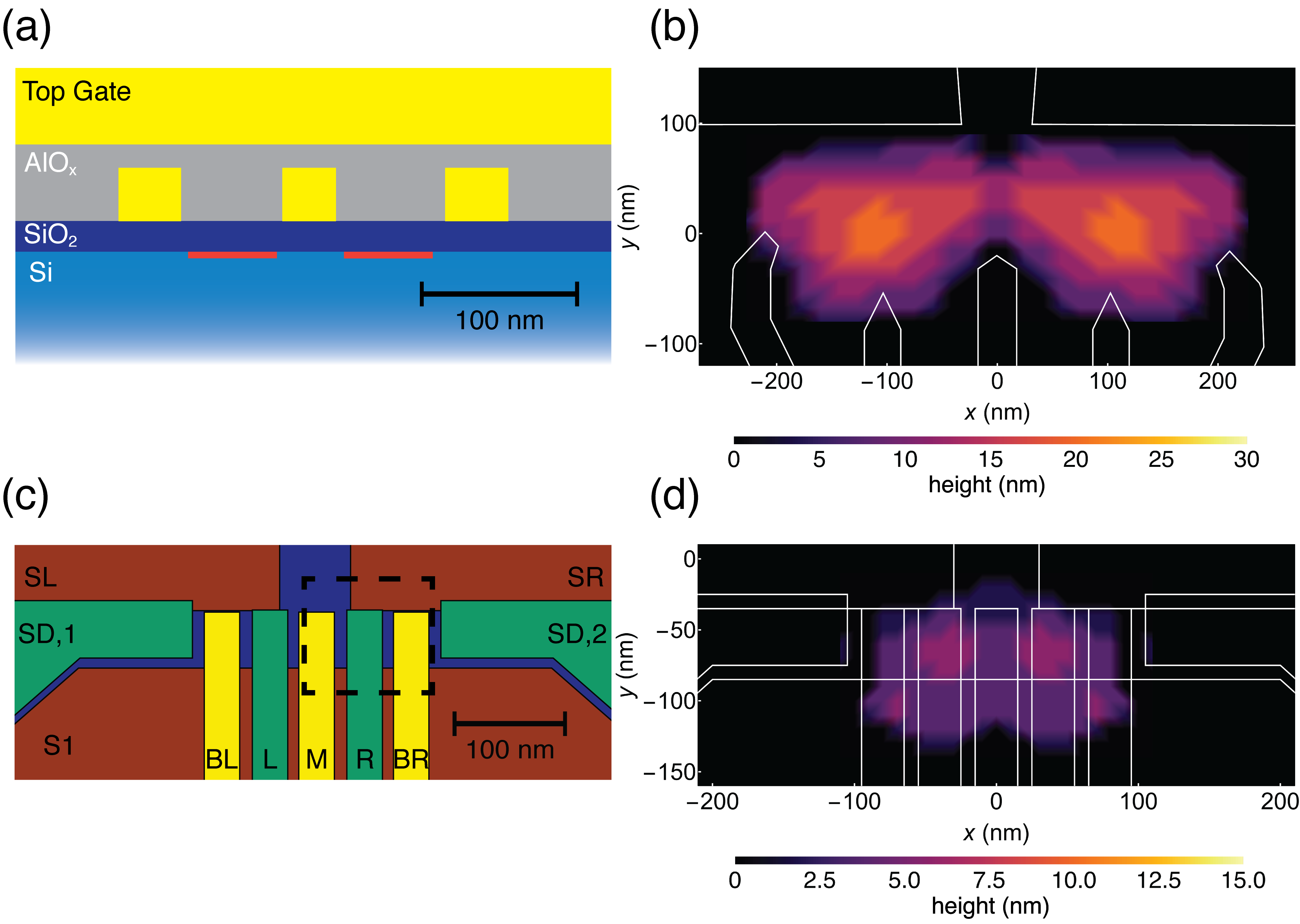
Ten nominally identical devices were fabricated and measured, each with a layer of SiO2. The Ti/Au electrostatic gates were created using electron-beam lithography, evaporation, and liftoff techniques. A conformal layer of aluminum oxide was then applied, followed by deposition of a global top gate. A scanning electron micrograph (SEM) of the essential part of a device, similar to those measured, is shown in Fig. 1(a). In this device architecture, the global top gate is used to accumulate electrons at the Si/SiO2 interface, and a double quantum dot (DQD) system is defined by applying appropriate voltages to seven of the confinement gates. A schematic of a device cross-section is shown in Fig. 1(b).
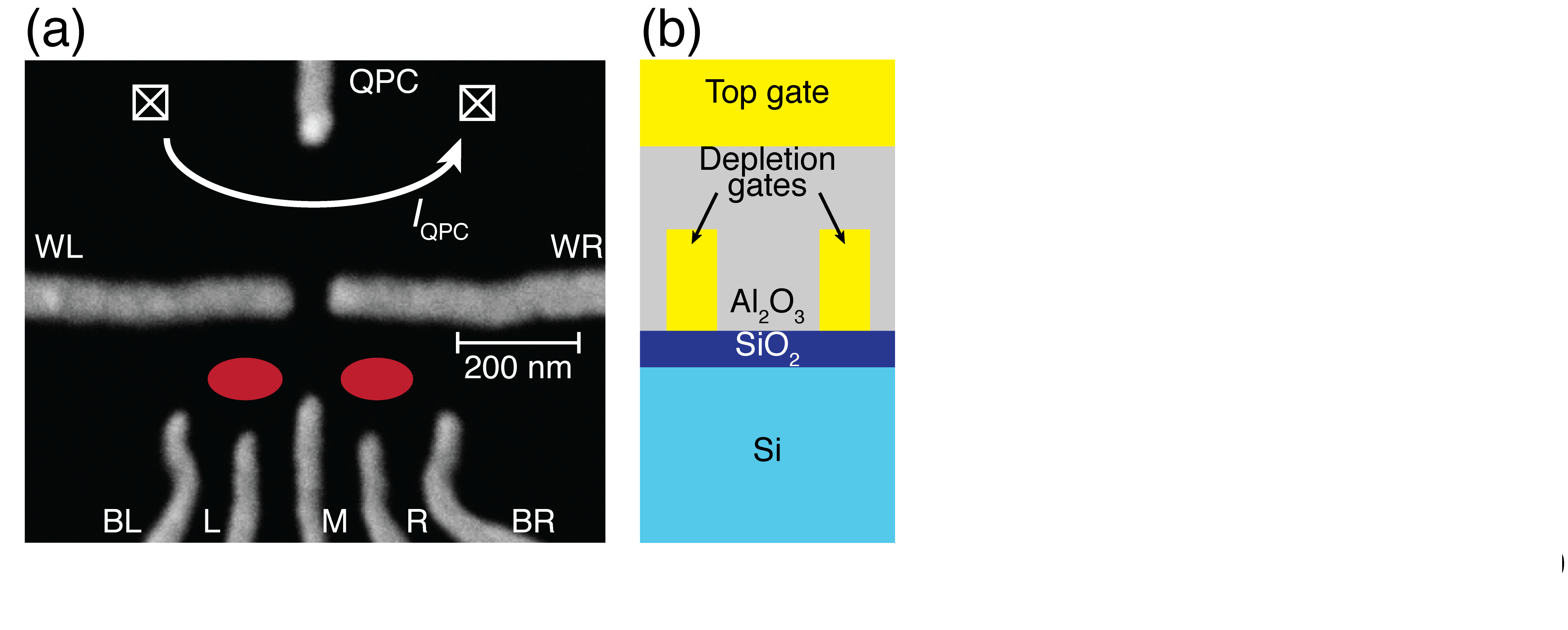
The devices are operated and measured in a dilution refrigerator operating at a base temperature of approximately . The dots are characterized by measuring the differential conductance through the quantum point contact (QPC); peaks in the differential conductance occur at voltages at which the occupation in a dot changes. Pulsed gate experiments are performed in magnetic fields, to further characterize the behavior of the samples, as described in Section III.
II.2 Theoretical Methods
Our theoretical calculations address the question of whether impurities in the oxide layer of these devices can induce unintentional levels that are not easily discernible in stability diagrams but which can cause spin blockade to be lifted. In our calculations we assume that all conduction band valley splittings are large and include only electrons in the lowest valley; this is consistent with experiment, since all devices studied here are confirmed to have valley splittings of at least (see Subsection III.1) – values that are consistent with Si-MOS devices reported in the literature Hao et al. (2014).
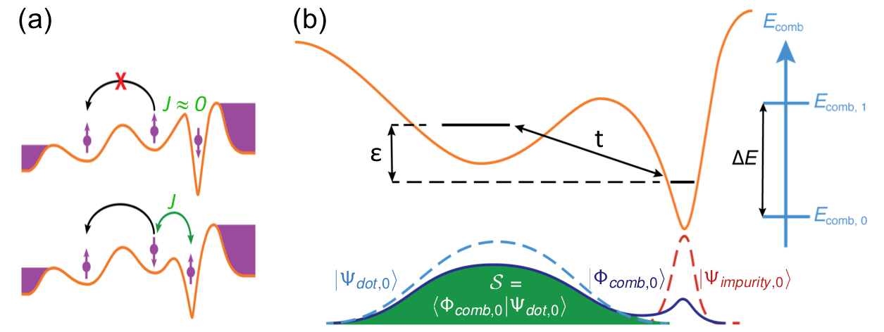
For impurity-induced levels to be a reasonable explanation for the experimental measurements, they must have large energy spacings, so that changes in occupation are not apparent in typical stability diagrams because the occupancy of the level does not change over the range of voltages investigated. This requirement implies that the electron wavefunctions in the impurity-induced level must be highly localized. At the same time, the electron in the impurity-induced level must have reasonably strong tunnel coupling to an electron in one of the lithographically defined dots, so that spin blockade is lifted via the process shown in Fig. 2(a). In this process, the electron in one of the lithographic dots can go into a singlet state in the already-occupied other dot while conserving all the spin quantum numbers of the three-electron system because the spin on the lithographic dot can flip due to exchange with an electron in the impurity-induced level. This behavior is closely related to processes that occur in other three-electron systems Shaji et al. (2008); Simmons et al. (2010); Koh et al. (2011), including the quantum dot hybrid qubit Shi et al. (2012); Cao et al. (2016).
A crucial ingredient of our theoretical investigation is to estimate the likelihood that a given device has an impurity-induced accidental level that is sufficiently strongly coupled to lift spin blockade. We note that for tunnel couplings that are small compared to the energy level detunings between the gate-defined dot and the impurity-induced level, the rate of virtual transfer of an electron into a singlet state in which one dot is doubly occupied is of order , where is the exchange coupling between the two levels. The exchange can be approximated as , as appropriate when is large compared to the charging energy of the dot. corresponds to a (1,1) ground state, where denotes electrons in the lithographic dot and electrons in the levels induced by the impurity. We compute this rate and compare it to the frequency of the square wave pulses used in the experiment to characterize spin blockade. To lift spin blockade, the electron occupying the impurity level need only be coupled to one of the intentional dots in the system.
The full theoretical approach, described below, involves performing simulations of the electrostatics and quantum confinement of electrons in the experimental device, both in the absence and presence of a charged impurity. The results of the simulations are used to determine under what conditions the impurity-induced levels are expected to be occupied. We also calculate the tunnel coupling of an electron between a lithographic dot and an impurity-induced level.
The theoretical method is summarized as follows. We first calculate the screened electrostatic potential and self-consistent charge distribution using Thomas-Fermi simulations, while adjusting the gate voltages to obtain single electron occupancy in each dot, once excluding and then including an impurity potential. The lowest two eigenstates of the single-particle 2D Schrödinger equation are then obtained for both cases. Section II.2.1 shows how the exchange coupling between an electron in a lithographic quantum dot and an electron in an impurity-induced state is extracted from these calculations. We perform the calculations at different possible impurity locations to be able to estimate the probability that an impurity is at a position that would lead to the lifting of spin blockade.
II.2.1 Calculation of Exchange Couplings
In this subsection we present our method for estimating and and thus obtaining , the exchange coupling between an electron in a lithographic dot and an electron in an impurity-induced level.
We first determine the amount of hybridization between the lithographic dot ground state and the impurity-induced level ground state in the combined confinement potential. Let be the unperturbed lithographic dot ground state, be the impurity level ground state, and be the hybridized ground eigenstate of the combined system. Assuming can be decomposed in terms of and , we apply a Hubbard model to estimate the detuning and tunnel couplings using the energy difference between the total system ground state and the lithographic-dot ground state, where is the energy of the -th eigenstate of the combined dot-impurity system. These parameters are depicted in Fig. 2(b).
A general form for the Hamiltonian of a two level system defined by the basis is given by the two-by-two matrix:
| (1) |
with the energy detuning between the two states of the system and the tunnel coupling between them. The eigenenergies of this system are and the general forms for real eigenvectors are
| (2) |
| (3) |
with the mixing angle between the lithographic dot and the impurity dot.
Using this model, we can compute the energy difference and the overlap integral . Inverting Eq. (1) transformed into the basis defined by Eqs. (2)-(3) for and using these variables yields
| (4) |
and
| (5) |
In general, it is possible that the ground state and the first excited state of the total perturbed system are not well described as combinations of the unperturbed ground states of the lithographic dot and the occupied impurity-induced level. The most common of these scenarios is when the impurity potential is weak enough that the combined system is almost identical to that of the unperturbed lithographic dot. These ill-defined scenarios have no impact in our estimations because we only take into account impurity configurations meeting certain criteria regarding the total electron energy and exchange coupling, as discussed later in Subsec. II.2.3.
II.2.2 Finite-Element Simulation Methods
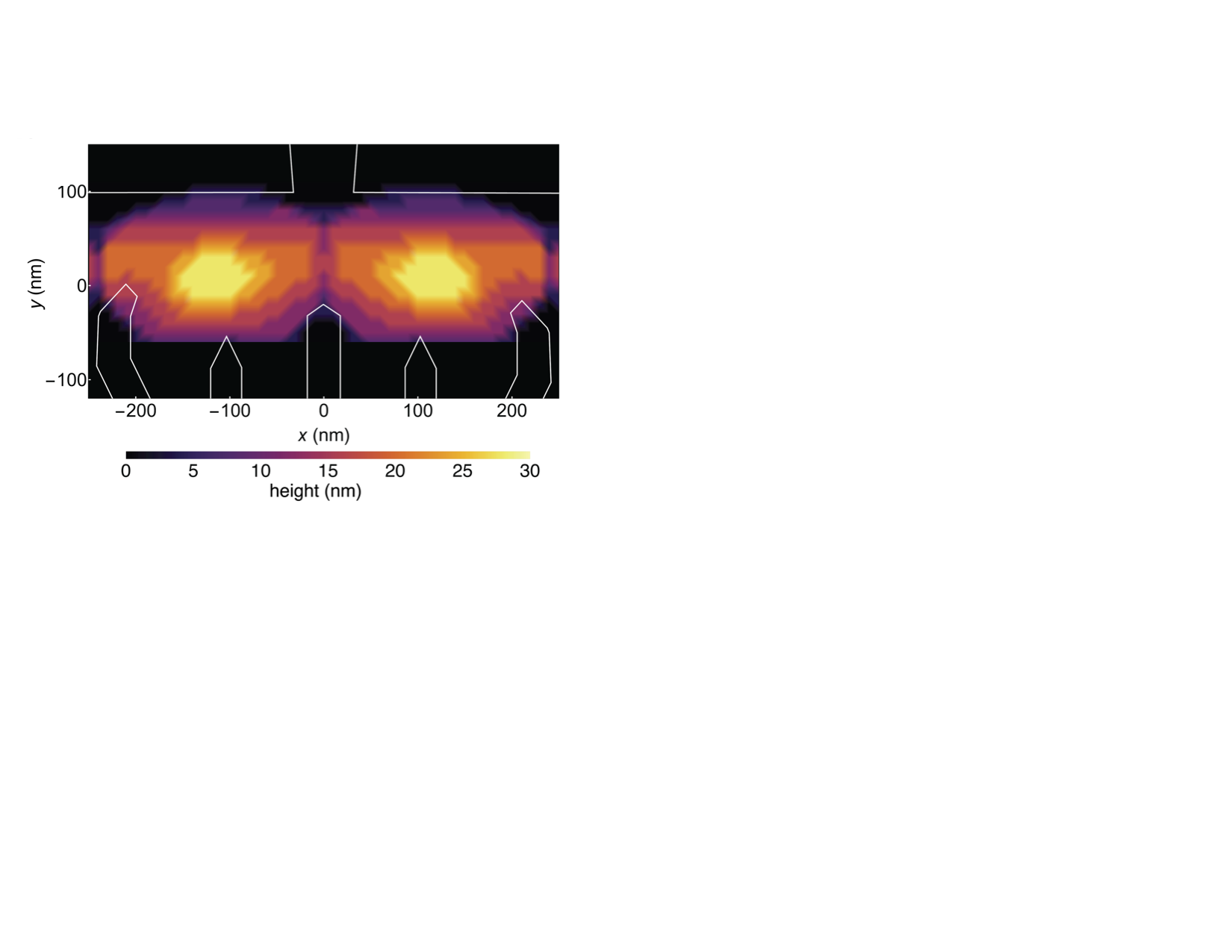
To determine whether typical Si-MOS devices possess large enough charge impurity densities to support the creation of spurious levels containing an electron capable of suppressing blockade, we perform numerical simulations. In addition to a simulation with no impurities present, we perform a series of calculations in which a singly-charged impurity is introduced near the active region of the device within the oxide layer above the interface (see Fig. 3(a)). Note that the simulations do not include an additional uniform oxide charge density, since it contributes only an overall shift to the device potentials. For each impurity location, we calculate the electron charge density and then estimate the exchange coupling that would exist between the lithographically-defined quantum dot and the induced spurious level.
We solve for the screened electrostatic potential and self-consistent charge distribution of a two-dimensional electron gas (2DEG) located at the Si/SiO2 interface using the Thomas-Fermi approximation Stopa (1996), which is described in Appendix A. The simulations are performed within COMSOL Multiphysics com , a finite element simulation suite. The simulations are repeated, while adjusting the gate voltages, until we obtain device tunings with approximately one electron in each dot. Such calculational methods been used successfully to model nanodevices; see, e.g., Refs. Shaji et al., 2008; Zhao et al., 2019. Figure 3(b) depicts the Thomas-Fermi electron density for a typical double-dot tuning including an impurity.
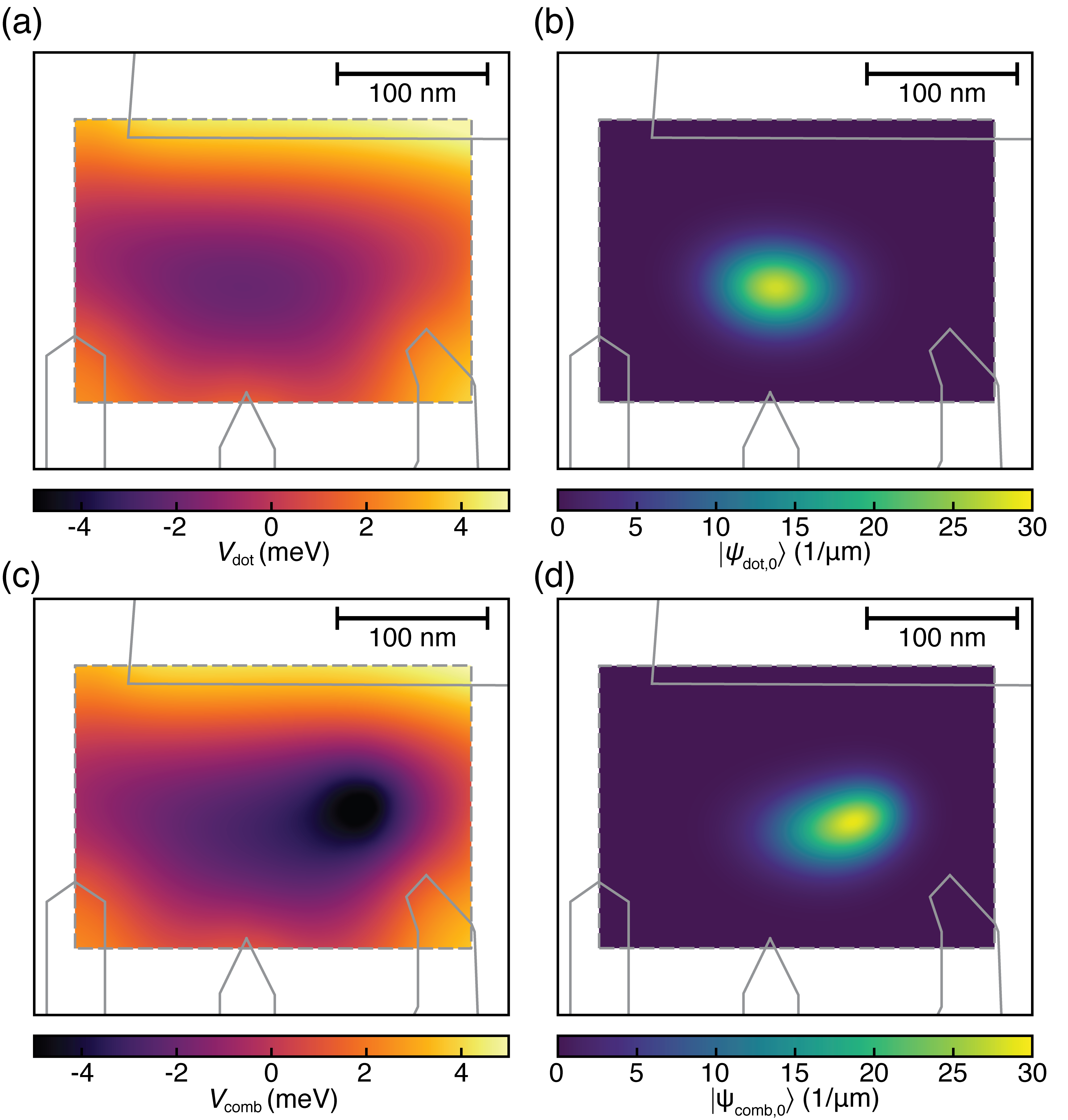
Exploiting the reflection symmetry of the device, we now focus on just the right quantum dot, where we calculate the two-dimensional (2D) electrostatic potential experienced by a single electron, in the plane of the 2DEG, . We introduce this confinement potential in a 2D Schrödinger equation for the right dot,
| (6) |
and solve to obtain the lowest two orbital eigenstates, . Here, is the transverse effective mass of a -valley in silicon. We further adjust the gate voltages such that the orbital energy splitting, , takes the experimentally reasonable value , while still satisfying the requirement of having one electron in each dot. The final gate voltages obtained through this procedure are listed in Appendix B. We also solve the Schrödinger equation for an electrostatic potential that includes a single point impurity with charge , in addition to the potentials from lithographically defined gates:
| (7) |
Here, and are the single-electron ground and excited states respectively of the combined dot-impurity system. Both and are computed in the Thomas-Fermi approximation for a realistic gate geometry, which simultaneously accounts for the image charges associated with the electrons in the lithographic dots, the 2DEG, the impurity potentials, and the nonlinear redistribution of charge density in the 2DEG, in response to changes in gate voltages and the position of the impurity.
Finally, we use the methods of Sec. II.2.1 to calculate the exchange coupling between an electron in a lithographically defined dot and in the impurity-induced level. In the current section, we obtain the inputs to this theory, including the orbital energy spacing, , and the overlap integral between the combined system ground state and the dot ground state (in the absence of an impurity), .
II.2.3 Calculation of “Dangerous” Impurity Locations
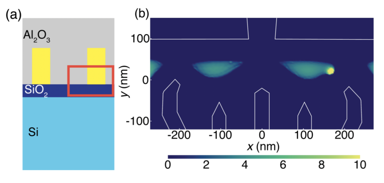
To map out “dangerous” regions, i.e., the possible locations at which impurities result in levels that lead to the lifting of spin blockade, we perform the calculations described in Secs. II.2.1 and II.2.2 on a grid of 5600 possible impurity locations throughout the active region of the device, above the 2DEG, amounting to a box of dimension (see Figure 3(a)), and we sort each location based on whether or not an impurity at that location would lead to the spin blockade lifting effects detailed above. The method used to estimate is only accurate when the electron in the spurious level is strongly bound, with a large energy level splitting to the excited state. Moreover, a weakly bound spurious level would be apparent in the experimentally measured stability diagram. Since such cases can be identified and corrected experimentally, by retuning the device, we include as one of our requirements for a “dangerous” impurity that . Additionally, since the square pulse frequencies in our experiments are approximately , we require a “dangerous” impurity to act faster than this, corresponding to a lower limit on of or . We then map out the impurity locations within the testing box shown in Figure 3(a) that meet these two requirements. In this way, we determine the lower limit of the impurity density that causes lifting of spin blockade with probability greater than .
III Results
In this section we discuss the experimental and theoretical results.
III.1 Experimental Results
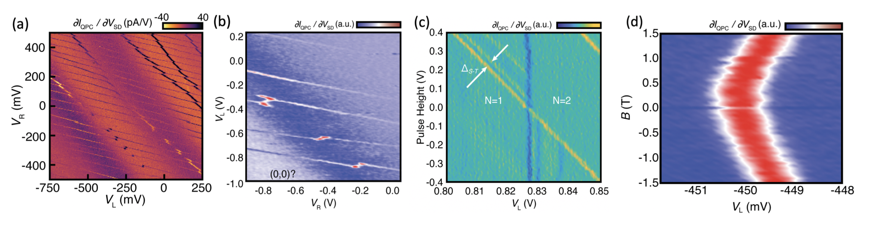
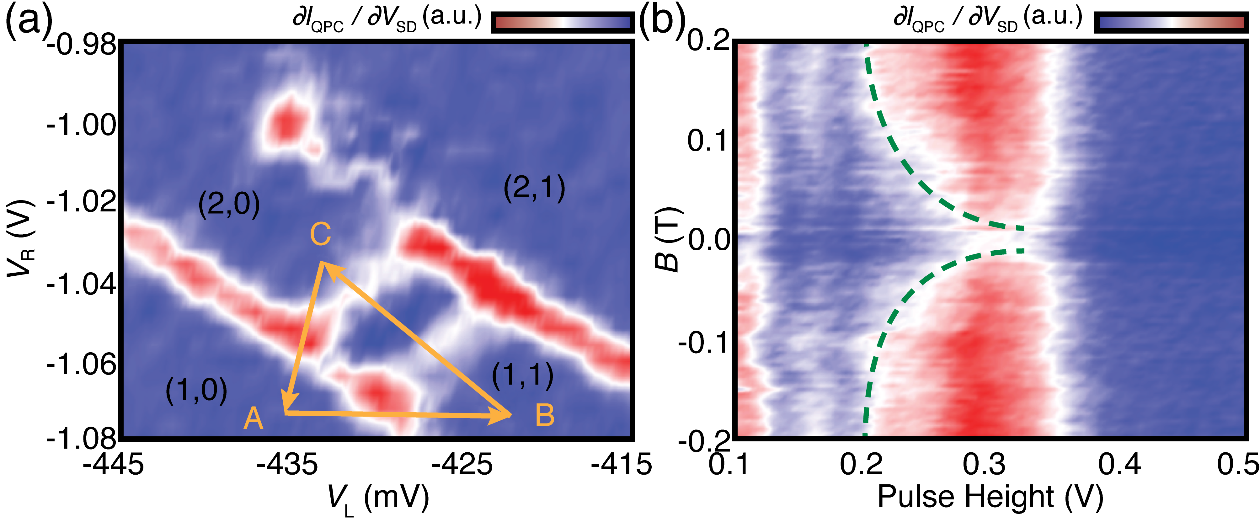
Figure 4(a) shows a stability diagram van der Wiel et al. (2002) in the few-electron regime with source-drain bias of , demonstrating the characteristic features of a double quantum dot: charging lines with two different slopes, that occur at voltages at which an electron is added to one of the dots.
For each of the ten devices examined, the voltages were tuned to create a double dot configuration and then depleted to low electron occupations, as shown in Fig. 4(b). Efforts were made to fully deplete the quantum dots; for example, all experiments testing for Pauli blockade were performed over multiple anti-crossings Jones et al. (2018). Using the voltage differences between the transition lines together with the relevant lever arms to estimate the dot capacitances Hanson et al. (2007), we find values consistent with single electron occupation. While we cannot definitely rule out the possibility of closed shells of electrons at the nominal (0,0) occupation, the presence of closed shells does not preclude the measurement of Pauli spin blockade, as has been demonstrated in Refs. Kodera et al., 2009; Harvey-Collard et al., 2017; Chen et al., 2017; Petit et al., 2019; Yang et al., 2019; Leon et al., 2020.
Excited state spectroscopy measurements Huebl et al. (2010); Xiao et al. (2010); Maune et al. (2012), shown in Fig. 4(c), were carried out to read the singlet-triplet splitting in each dot of every device. In these experiments, a square pulse with frequency approximately equal to the tunneling rate (a few hundred ) was applied in combination with an average (DC) voltage shift on gate L, to populate the excited states of the quantum dot. The energy difference between the ground and first excited states, corresponding to the singlet-triplet splitting , was consistently found to be between 100 and , using lever arms determined in the magnetospectroscopy experiments, as described below. (A lever arm describes the conversion factor between a gate voltage and a relevant dot energy.) Despite these large singlet-triplet splittings, spin blockade was not observed in nine out of ten devices. Results from the tenth device, which did exhibit spin blockade, are presented in Appendix C.
Magnetospectroscopy experiments were conducted with the magnetic field oriented parallel to the dot axis on three devices. Figure 4(d) shows magnetospectroscopy data used to determine gate lever arms in one device; these data also demonstrate that the singlet-triplet splitting in the device is substantial, because increasing the magnetic field makes it energetically less favorable to add a new electron to form a singlet state; this allows us to unambiguously identify the ground two-electron state as a singlet Hanson et al. (2007).
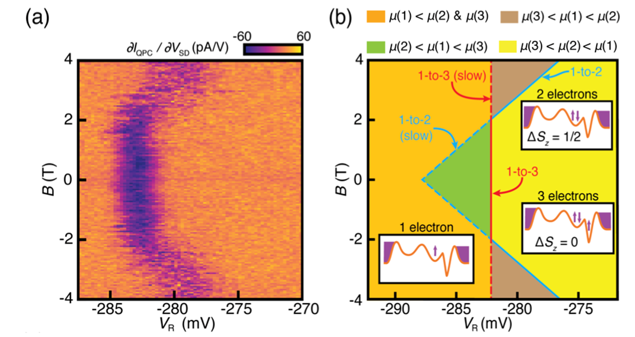
While typical magnetospectroscopy data are shown in Fig. 4(d), one region of the stability diagram of one sample exhibited anomalous behavior, as shown in Fig. 5(a), where the -dependent line segments normally correspond to a charging transition from 1-to-2 electrons (see Fig 5(b)). In this case, the transition has an unexpected segment that is independent of magnetic field. Including the presence of an occupied impurity-induced level provides a natural explanation for this behavior: the vertical line would correspond to a 1-to-3 electron transition with . This simultaneous change of occupation of a lithographic dot and impurity level is rare because the voltage range in a typical experimental sweep is not sufficient to change the occupation of the impurity level.
Figure 5(b) shows possible energy orderings of states with 1, 2, and 3 electrons, as pictured in the insets, for a system with one dot and an impurity level. The figure contains shaded regions that correspond to different energy orderings, which are discussed in detail in Appendix D. Charging transitions to states with more electrons occur as the gate voltage becomes less negative. In magnetospectroscopy experiments, we would normally expect the transition to the three-electron configuration to occur on the far-right-hand side of the diagram, although its exact location depends on the relative sizes of the Zeeman, orbital and charging energy terms. In particular, if the quantum dot confinement potential is weak and an extra level is present, then the charging energy for adding two electrons can be small, bringing the 1-to-3 electron transition into the measurement window, as indicated in Fig. 5(b). While we do not measure the individual energy terms here, Appendix D demonstrates that reasonable values of the system parameters are consistent with the transitions observed in Fig. 5(a). [The parameters listed in Appendix D are used to plot Fig. 5(b).] The pattern of the transition line is reproduced if one assumes that the 1-to-2 transition rate becomes unobservably slow when the voltage is made more negative and the 1-to-3 transition rate also becomes slower as the magnetic field is increased. Such dependencies are not unexpected, because tunnel rates typically decrease as depletion gate voltages are made more negative, and a decrease in wave function overlap between the dot and the impurity level is expected due to magnetic confinement.
III.2 Theoretical Results
Our simulations reveal some trends of interest. First, negative charges rarely induce unintentional levels, except when the impurity is within of the 2DEG and close to the center of a lithographically defined dot. In contrast, positively charged impurities in many different locations in the oxide induce impurity levels that can lift spin blockade, as shown in Fig. 6. There is a large region directly over the 2DEG where placement of a positively charged impurity induces an occupied impurity level with a tightly bound state that also has a strong enough exchange coupling that spin exchange occurs on a timescale less than with a nearby gate-defined dot. If we assume one electron within this volume, we find that a uniform impurity density of causes lifting of spin blockade with high probability. The Si/SiO2 interface is a region of concern for MOS-based spin qubits and if we consider the sampled locations nearest to this interface, we find a uniform surface impurity density of would likely result in an impurity occurring within the spin-blockade lifting area. This density is on the low end of the expected impurity densities for these devices Sakaki et al. (1970) – approximately in high quality thermal oxides Kim et al. (2017). Comparing the calculated threshold and the expected value suggests a high likelihood of spin blockade being absent from these devices.
We stress that the analysis presented here focuses on fixed oxide charges, which are only one particular class of Si/SiO2 interface traps. A direct comparison between this charge density threshold and typical values of densities of interface traps (as measured in cm-2 eV-1 by CV methods, for instance) may not be direct, requiring further identification of the physical mechanism behind the different traps. Other trapping mechanisms, such as fast interface states and chemical bonding faults right at the Si/SiO2 interface are also likely to affect the spin state of qubits, but are out of the scope of the current work.
Modifying the gate geometry to increase the screening of the oxide layer reduces the likelihood that spin-blockade lifting occurs via this mechanism. To demonstrate this, we examine two modifications to the gate structure: moving the global top gate from above the 2DEG to , and altering the gate layout to an overlapping gate design similar in layout to that used in a Si-MOS deviceVeldhorst et al. (2014, 2015). The details of the gate layout we consider are adapted from a device fabricated on Si/SiGe Zajac et al. (2016). (Further details on gate geometries studied here are provided in Appendices B and E.) Generally, we find that using an overlapping gate design has the largest impact on our results, due to the compact coverage of metallic gates directly above the 2DEG and the overall tighter confinement of the lithographically defined dots compared to the original device considered. The likelihood that spin blockade is lifted is found to decrease, as quantified by the impurity density threshold increasing by a factor of eighteen, while the interface impurity density threshold increases by a factor of three. Increasing accumulation gate voltages could also increase the likelihood of observing spin blockade because this increases confinement within a dot, which in turn reduces the wavefunction overlap between the lithographic dot and an occupied impurity-induced level. Another route for increasing the device yield is to improve the quality of the oxide, particularly at the Si/SiO2 interface, since this reduces the number of charges in close proximity to the lithographically-defined quantum dots. Finally, moving the active region of the device further away from the impurities, by using a Si/SiGe heterostructure for example, also reduces the likelihood of forming dangerous impurity dots.
IV Discussion
Our measurements and calculations indicate that failure to observe spin blockade in a substantial fraction of Si-MOS double quantum dot devices with large singlet-triplet splittings could arise because of additional energy levels induced by impurities in the oxide of the devices. We show that in the samples we investigated, there is a reasonable probability that unintentional levels produced by trapped positive charges in the oxide layer have large enough binding energies that they would not typically be apparent in charge stability diagrams, and yet their exchange coupling to one of the lithographically defined dots is large enough to cause suppression of spin blockade. Typical densities of defects in these devices are consistent with the observations.
This problem can be mitigated not only by altering fabrication methods to reduce the number of charged defects in the device oxide. Our calculations indicate that employing device designs in which metal gates are positioned directly over the dots, which enhances the screening of the impurity levels, also can mitigate the problem substantially.
Acknowledgements.
The authors thank M. Eriksson, A. Frees, and J. S. Kim for useful comments and discussions. This work was supported by ARO (W911NF-12-1-0607, W911NF-17-1-0274, W911NF-14-1-0346, W911NF-17-1-0242, W911NF-12-1-0609, W911NF-17-1-0257), NSF (OISE-1132804), the Department of Defense under Contract No. H98230-15-C0453, MEIC (Spain) FIS2012-33521 and FIS2015-64654-P, CSIC (Spain) Research Platform PTI-001, and CNPq (Brazil) 309861/2015-2 and 304869/2014-7. The authors acknowledge support from the Vannevar Bush Faculty Fellowship program sponsored by the Basic Research Office of the Assistant Secretary of Defense for Research and Engineering and funded by the Office of Naval Research through grant N00014-15-1-0029. The views and conclusions contained in this document are those of the authors and should not be interpreted as representing the official policies, either expressed or implied, of the U.S. Government. The U.S. Government is authorized to reproduce and distribute reprints for Government purposes notwithstanding any copyright notation herein.Appendix A Details of Thomas-Fermi Simulations
In this appendix, we present additional details of the Thomas-Fermi simulations.
As described in the main text, we performed simulations of either two electrons in a lithographically defined double quantum dot, or three electrons in a double dot system, with an additional impurity-induced level. To begin, we treat the double dot two-electron system semi-classically as described below.
The three-dimensional (3D) finite element simulations are conducted on a by section of the active region of the device. The device stack consists of of silicon, of SiO2 and of Al2O3. The boundary conditions used in all 3D models are as follows. The bottom surface of the device is set to ; for all other boundaries, we apply the conditions , where is the electric displacement field and the unit normal at the surface. In all cases, the simulation cell boundary was chosen large enough that the exact position of the boundaries had no effect on our results.
We first determine a set of gate voltages, as listed in Appendix B, which cause approximately one electron to accumulate in each dot. (Since this is a semi-classical calculation, electron quantization must be enforced by hand.) The 2DEG for this system is assumed to form at the Si/SiO2 interface and the charge density is calculated self-consistently by applying the Thomas-Fermi approximation Stopa (1996) to model the areal charge density , using the following definition:
| (8) |
where is the 2D transverse effective mass of a -valley electron in silicon and is the spatially varying electrostatic potential at the position of the 2DEG. Here, we assume the valley splitting is large enough that we only need to consider one valley state. In Eq. (8), we define the electron Fermi level to occur at .
As described in the main text, the results of the Thomas-Fermi electrostatics simulations are evaluated in the plane of the 2DEG, and input into two-dimensional (2D) Schrödinger equations. The full procedure is repeated, with and without introducing an impurity into the device, and considering a 3D grid of impurity locations. Some typical electrostatic and quantum simulation results are shown in Fig. 7, for the right-hand dot.
Appendix B Gate Voltage Tables
In this appendix, we list the gate voltages used in our simulations, which were chosen to accumulate one electron in each dot, while maintaining an orbital excitation energy in the right dot corresponding to 0.5 meV. The three tables provide the voltages used for the gate geometry used in the experiment, for a geometry similar to that used in the experiment except that the global top gate is moved 50 nm closer to the 2DEG, and for an overlapping gate design similar to the one used in Ref. Zajac et al., 2016.
| Gate | Voltage () |
|---|---|
| 98 | |
| -250 | |
| -14.4 | |
| -14.4 | |
| -8 | |
| -10 | |
| -10.4 | |
| -10 | |
| -8 |
| Gate | Voltage () |
|---|---|
| 45 | |
| -150 | |
| -30 | |
| -30 | |
| -34 | |
| -5 | |
| -40 | |
| -5 | |
| -32 |
| Gate | Voltage () |
|---|---|
| 0 | |
| -60 | |
| -60 | |
| 400 | |
| 400 | |
| -12 | |
| 235 | |
| -7 | |
| 235 | |
| -12 |
Appendix C Experimental Evidence for Spin Blockade in One Device
A search for Pauli blockade via a three-pulse sequence Jones et al. (2018) was conducted for ten devices. This appendix reports the data demonstrating the presence of Pauli spin blockade in one device. Fig. 8(a) shows a portion of a stability diagram taken in the presence of a pulse pattern consisting of three sequences generated on an arbitrary waveform generator with two channels controlling the voltage on gate L and R; the details of the sequence are shown in Fig. 8(a). The splitting of the polarization line shown in Fig. 8(a) demonstrates that there are two different voltages at which an electron transfers between the dots, which arises because Pauli spin blockade implies that a portion of the time the two-electron state is a triplet, which has a higher energy than the singlet. Moreover, a spin funnel is also observed (see Fig. 8(b) Petta et al. (2005)), which arises because of the change of electron transfer between the dots at the anticrossing between the singlet and polarized triplet, the visibility of which relies on spin blockade.
Appendix D Additional Discussion of Anomalous Magnetospectroscopy Results
In this appendix we provide a detailed discussion of our interpretation of the anomalous magnetospectroscopy data presented in Fig. 5 using our model that includes an impurity-induced level. We do this by relating the slopes of the transition lines in the stability diagram to the energetics of the system with up to three electrons. The intuition behind the argument is that the most straightforward way to obtain a magnetic-field-independent voltage at which the charge in the system changes is to have the charge occupation change by two electrons, and such a change can occur if there is a significant exchange interaction between the two electrons that are added.
We use a simple Hubbard model to calculate the chemical potential for up to three electrons occupying a system consisting of a lithographic quantum dot and an impurity-induced level. Let be the chemical potential of electrons in the combined system. These chemical potentials have several dominant contributions, given by
| (9) | |||
| (10) | |||
| (11) |
where is the effect of Coulomb repulsion on the total system due to the previous electrons, is the lever arm of the dot, is the lever arm of the impurity, is the exchange energy that between the dot and the impurity for the three electron state, is the voltage on the gate, is the Landé -factor for silicon, and is the Bohr magneton. We assume that the one electron state is initialized in the spin down (up) state for positive (negative) applied magnetic field, the two electron state corresponds to a singlet in a single dot for the range of fields studied, and that the three electron state initializes in the manifold with total spin and -component spin down (up) based on positive (negative) applied field. Using the parameter values in Table 4, we find the energy regions shown in Fig. 5(b). The value of was set by the slope of the data in Fig. 5(a). The remaining parameters were tuned to values that reproduce the magnetospectroscopy in Fig. 4(d) of the main text. Visually similar behavior can be found for different parameter choices. As a note, for this set of parameters, we also observe a small region where , which outside the voltage range plotted in Fig. 4(d). We assume that the same slow tunnel rate that makes the 1-to-2 transition invisible, as discussed in the main text, also suppresses transitions to this two-electron ground state.
| Parameter | Value |
|---|---|
| 2.1 | |
Appendix E Calculations for Modified Gate Designs
Here we investigate gate designs that differ from the one used for the samples studied in the main text. We find that changing the gate geometry can change substantially the size and shape of the region where placement of an impurity is likely to induce a level containing a spin blockade lifting electron.
We examined two modifications to the device design: (i) one in which the top gate was moved closer to the 2DEG, reducing the separation between the global top gate from to , and (ii) the other consisted of replacing the stadium style gates by an overlapping gate design similar to that used in Ref. Zajac et al., 2016. This style of design consists of three layers of gates: the first is a screening layer that defines the dot channels, the second layer consists of depletion gates, and the third layer consists of accumulation gates. Separating the layers is a conformal layer of Al2O3. The devices we simulate are shown in Fig. 9. Both changes would increase screening of charged impurities in the oxide and are expected to increase the minimum impurity density to lift spin blockade.
For the close-proximity top gate simulation, we considered charged impurities in the same region as for the calculations summarized by Fig. 3 of the main text. For the analysis of the overlapping gate geometry, we considered a box with dimensions, centered under the right accumulation gate starting at the 2DEG interface and going up into the oxide, with a total of 1120 charge locations, as indicated in Fig. 9(c). The overlapping gate design defines smaller dots and typically has a larger orbital energy splitting than the stadium style designs. The energy cutoff for this design was chosen to be , approximately twice the orbital energy splitting measured in Ref. Zajac et al., 2016. Gate voltages that yield dots with single occupancy for the different designs are tabulated in Appendix B.
In the following, we consider an impurity location dangerous if an impurity at that location leads to the spin blockade lifting effects discussed in the main text. In the closer top gate design modification, the lateral features of the dangerous region are largely unchanged, but the maximum height of that region is reduced by a factor of two. The volume of dangerous impurity locations is , as shown in Fig. 9(b), which represents a slight improvement on the original device, and a uniform impurity density of would yield a high probability of finding one impurity within this spin-blockade lifting volume. Considering only the charges at the interface, the area of dangerous impurity locations is . With a single charge within this area, the dangerous impurity density at the interface is . This increase in surface density represents a slight improvement on the original device.
The overlapping gate design greatly reduced the dangerous region. This can be attributed to the increased screening as well as the more tightly confined dots inherent to this closely packed gate design, as this close confinement reduces the wavefunction overlap between the lithographic dot and the impurity level. The volume of spin-blockade lifting impurity locations, shown in Fig. 9(d), is , and the impurity number density corresponding to one impurity within this volume is . This increase in density represents a factor of eighteen improvement in densities at which we would expect to start seeing spin blockade lifting effects. Considering only charges at the interface, the dangerous impurity area is and the corresponding dangerous surface density is . This limit on the interface impurity density, while improved from the devices described in Fig. 3 of the main text, is still lower than the expected impurity density Sakaki et al. (1970); Kim et al. (2017) indicating that we would still expect to see spin blockade lifting effects in these devices.
References
- Loss and DiVincenzo (1998) D. Loss and D. P. DiVincenzo, Phys. Rev. A 57, 120 (1998).
- Zwanenburg et al. (2013) F. A. Zwanenburg, A. S. Dzurak, A. Morello, M. Y. Simmons, L. C. L. Hollenberg, G. Klimeck, S. Rogge, S. N. Coppersmith, and M. A. Eriksson, Rev. Mod. Phys. 85, 961 (2013).
- Tyryshkin et al. (2012) A. M. Tyryshkin, S. Tojo, J. J. L. Morton, H. Riemann, N. V. Abrosimov, P. Becker, H.-J. Pohl, T. Schenkel, M. L. W. Thewalt, K. M. Itoh, and S. A. Lyon, Nat. Mater. 11, 143 (2012).
- Veldhorst et al. (2014) M. Veldhorst, J. C. C. Hwang, C. H. Yang, A. W. Leenstra, B. de Ronde, J. P. Dehollain, J. T. Muhonen, F. E. Hudson, K. M. Itoh, A. Morello, and A. S. Dzurak, Nat. Nanotechnol. 9, 981 (2014).
- Veldhorst et al. (2015) M. Veldhorst, C. H. Yang, J. C. C. Hwang, W. Huang, J. P. Dehollain, J. T. Muhonen, S. Simmons, A. Laucht, F. E. Hudson, K. M. Itoh, A. Morello, and A. S. Dzurak, Nature 526, 410 (2015).
- Jock et al. (2018) R. M. Jock, N. T. Jacobson, P. Harvey-Collard, A. M. Mounce, V. Srinivasa, D. R. Ward, J. Anderson, R. Manginell, J. R. Wendt, M. Rudolph, T. Pluym, J. K. Gamble, A. D. Baczewski, W. M. Witzel, and M. S. Carroll, Nat. Comm. 9, 1768 (2018).
- Levy (2002) J. Levy, Phys. Rev. Lett. 89, 147902 (2002).
- Petta et al. (2005) J. R. Petta, A. C. Johnson, J. M. Taylor, E. A. Laird, A. Yacoby, M. D. Lukin, C. M. Marcus, M. P. Hanson, and A. C. Gossard, Science 309, 2180 (2005).
- Ciorga et al. (2000) M. Ciorga, A. S. Sachrajda, P. Hawrylak, C. Gould, P. Zawadzki, S. Jullian, Y. Feng, and Z. Wasilewski, Phys. Rev. B 61, R16315 (2000).
- Ono et al. (2002) K. Ono, D. G. Austing, Y. Tokura, and S. Tarucha, Science 297, 1313 (2002).
- Hao et al. (2014) X. Hao, R. Ruskov, M. Xiao, C. Tahan, and H. Jiang, Nat. Comm. 5, 344 (2014).
- Maune et al. (2012) B. M. Maune, M. G. Borselli, B. Huang, T. D. Ladd, P. W. Deelman, K. S. Holabird, A. A. Kiselev, I. Alvarado-Rodriguez, R. S. Ross, A. E. Schmitz, M. Sokolich, C. A. Watson, M. F. Gyure, and A. T. Hunter, Nature 481, 344 (2012).
- Wu et al. (2014) X. Wu, D. R. Ward, J. R. Prance, D. Kim, J. K. Gamble, R. T. Mohr, Z. Shi, D. E. Savage, M. G. Lagally, M. Friesen, S. N. Coppersmith, and M. A. Eriksson, Proc. Natl. Acad. Sci. U.S.A. 111, 11938 (2014).
- Harvey-Collard et al. (2017) P. Harvey-Collard, N. T. Jacobson, M. Rudolph, J. Dominguez, G. A. Ten Eyck, J. R. Wendt, T. Pluym, J. K. Gamble, M. P. Lilly, M. Pioro-Ladrière, and M. S. Carroll, Nat. Comm. 8, 1029 (2017).
- Veldhorst et al. (2017) M. Veldhorst, H. G. J. Eenink, C. H. Yang, and A. S. Dzurak, Nature Comm. 8, 1766 (2017).
- Xiao et al. (2010) M. Xiao, M. G. House, and H. W. Jiang, Phys. Rev. Lett. 104, 096801 (2010).
- Maurand et al. (2016) R. Maurand, X. Jehl, D. Kotekar-Patil, A. Corna, H. Bohuslavskyi, R. Laviéville, L. Hutin, S. Barraud, M. Vinet, M. Sanquer, and S. De Franceschi, Nat. Comm. 7, 13575 (2016).
- Zajac et al. (2016) D. M. Zajac, T. M. Hazard, X. Mi, E. Nielsen, and J. R. Petta, Phys. Rev. Applied 6, 054013 (2016).
- Shaji et al. (2008) N. Shaji, C. B. Simmons, M. Thalakulam, L. J. Klein, H. Qin, H. Luo, D. E. Savage, M. G. Lagally, A. J. Rimberg, R. Joynt, M. Friesen, R. H. Blick, S. N. Coppersmith, and M. A. Eriksson, Nat. Phys. 4, 540 (2008).
- Simmons et al. (2010) C. B. Simmons, T. S. Koh, N. Shaji, M. Thalakulam, L. J. Klein, H. Qin, H. Luo, D. E. Savage, M. G. Lagally, A. J. Rimberg, R. Joynt, R. Blick, M. Friesen, S. N. Coppersmith, and M. A. Eriksson, Phys. Rev. B 82, 245312 (2010).
- Koh et al. (2011) T. S. Koh, C. B. Simmons, M. A. Eriksson, S. N. Coppersmith, and M. Friesen, Phys. Rev. Lett. 106, 186801 (2011).
- Shi et al. (2012) Z. Shi, C. B. Simmons, J. R. Prance, J. K. Gamble, T. S. Koh, Y.-P. Shim, X. Hu, D. E. Savage, M. G. Lagally, M. A. Eriksson, M. Friesen, and S. N. Coppersmith, Phys. Rev. Lett. 108, 140503 (2012).
- Cao et al. (2016) G. Cao, H.-O. Li, G.-D. Yu, B.-C. Wang, B.-B. Chen, X.-X. Song, M. Xiao, G.-C. Guo, H.-W. Jiang, X. Hu, , and G.-P. Guo, Physical Review Letters 116, 086801 (2016).
- Stopa (1996) M. Stopa, Phys. Rev. B 54, 13767 (1996).
- (25) COMSOL Multiphysics® v. 5.3a. www.comsol.com. COMSOL AB, Stockholm, Sweden.
- Zhao et al. (2019) R. Zhao, T. Tanttu, K. Y. Tan, B. Hensen, K. W. Chan, J. Hwang, R. Leon, C. H. Yang, W. Gilbert, F. Hudson, K. Itoh, A. Kiselev, T. Ladd, A. Morello, A. Laucht, and A. Dzurak, Nature Communications 10, 1 (2019).
- van der Wiel et al. (2002) W. G. van der Wiel, S. De Franceschi, J. M. Elzerman, T. Fujisawa, S. Tarucha, and L. P. Kouwenhoven, Rev. Mod. Phys. 75, 1 (2002).
- Jones et al. (2018) A. M. Jones, E. J. Pritchett, E. H. Chen, T. E. Keating, R. W. Andrews, J. Z. Blumoff, L. A. De Lorenzo, K. Eng, S. D. Ha, A. A. Kiselev, S. M. Meenehan, S. T. Merkel, J. A. Wright, L. F. Edge, R. S. Ross, M. T. Rakher, M. G. Borselli, and A. Hunter, ArXiv e-prints (2018), arXiv:1809.08320 [quant-ph] .
- Hanson et al. (2007) R. Hanson, L. Kouwenhoven, J. Petta, S. Tarucha, and L. Vandersypen, Reviews of Modern Physics 79, 1217 (2007).
- Kodera et al. (2009) T. Kodera, K. Ono, S. Amaha, Y. Arakawa, and S. Tarucha, in Journal of Physics: Conference Series, Vol. 150 (IOP Publishing, 2009) p. 022043.
- Chen et al. (2017) B.-B. Chen, B.-C. Wang, G. Cao, H.-O. Li, M. Xiao, G.-C. Guo, H.-W. Jiang, X. Hu, and G.-P. Guo, Physical Review B 95, 035408 (2017).
- Petit et al. (2019) L. Petit, H. Eenink, M. Russ, W. Lawrie, N. Hendrickx, J. Clarke, L. Vandersypen, and M. Veldhorst, arXiv preprint arXiv:1910.05289 (2019).
- Yang et al. (2019) C. Yang, R. Leon, J. Hwang, A. Saraiva, T. Tanttu, W. Huang, J. C. Lemyre, K. Chan, K. Tan, F. Hudson, K. Itoh, A. Morello, M. Pioro-Ladrière, A. Laucht, and A. Dzurak, ArXiv e-prints (2019), arXiv:1902.09126 .
- Leon et al. (2020) R. Leon, C. H. Yang, J. Hwang, J. C. Lemyre, T. Tanttu, W. Huang, K. W. Chan, K. Tan, F. Hudson, K. Itoh, A. Morello, A. Lauch, M. Pioro-Ladrière, A. Saraiva, and D. AS, Nature Communications 11, 1 (2020).
- Huebl et al. (2010) H. Huebl, C. D. Nugroho, A. Morello, C. C. Escott, M. A. Eriksson, C. Yang, D. N. Jamieson, R. G. Clark, and A. S. Dzurak, Physical Review B 81, 235318 (2010).
- Sakaki et al. (1970) H. Sakaki, K. Hoh, and T. Sugano, IEEE Trans. Electron Devices 17, 892 (1970).
- Kim et al. (2017) J. S. Kim, A. M. Tyryshkin, and S. A. Lyon, Appl. Phys. Lett. 110, 123505 (2017).