Highly enriched 28Si reveals remarkable optical linewidths and fine structure for well-known damage centers
Abstract
Luminescence and optical absorption due to radiation damage centers in silicon has been studied exhaustively for decades, but is receiving new interest for applications as emitters for integrated silicon photonic technologies. While a variety of other optical transitions have been found to be much sharper in enriched 28Si than in natural Si, due to the elimination of inhomogeneous isotopic broadening, this has not yet been investigated for radiation damage centers. We report results for the well-known G, W and C damage centers in highly enriched 28Si, with optical linewidth improvements in some cases of over two orders of magnitude, revealing previously hidden fine structure in the G center emission and absorption. These results have direct implications for the linewidths to be expected from single center emission, even in natural Si, and for models for the G center structure. The advantages of 28Si can be readily extended to the study of other radiation damage centers in Si.
I Introduction
A multitude of radiation damage centers in Si, with highly reproducible optical emission and absorption lines, have been studied exhaustively using a wide variety of techniques over the past 50+ years Davies (1989). Some of these centers produce very bright luminescence, and have recently received renewed interest as possible electrically-pumped light emitters, and single photon sources, compatible with an integrated silicon photonic technology Shainline and Xu (2007); Buckley et al. (2017); Beaufils et al. (2018). Previous high resolution studies of these centers in natural Si have shown reproducible limiting linewidths of typically greater than 0.04 meV, and it has become widely assumed that these relatively narrow linewidths represent some kind of fundamental limit for these centers. A wide variety of other optical transitions in Si have been shown to become remarkably sharper in 28Si than in natural Si (natSi) due to the elimination of the inhomogeneous broadening resulting from the mixture of the three stable Si isotopes (28Si, 29Si, 30Si) present in natSi Karaiskaj et al. (2001); Cardona and Thewalt (2005); Steger et al. (2009, 2012); Morse et al. (2017), but until now no studies of radiation damage centers have been undertaken in highly enriched 28Si. While
there have been studies of radiation damage centers in 30Si, that material was not as highly enriched as the available 28Si, and in addition was grown by the Czochralski process, with the high oxygen concentration resulting in additional inhomogeneous broadening, so no linewidth improvements over natSi were observed Hayama et al. (2004a, b).
Here we report on optical emission and absorption studies on three well-known damage centers produced in very high purity Si enriched to 99.995 28Si as part of the Avogadro project P. et al. (2009). All three emit in or near important optical communication bands: the C center (790 meV, or 1571 nm, thought to contain an interstitial C (Ci) and an interstitial O (Oi) Wagner et al. (1984); Davies et al. (1986, 1987a); Trombetta and Watkins (1987); Kürner et al. (1989); Bohnert et al. (1993)), the G center (969 meV, or 1280 nm, thought to contain a substitutional C (Cs), Ci, and an interstitial Si (Sii) Davies et al. (1987a); Canham et al. (1987); Song et al. (1990); Beaufils et al. (2018)), and the W center (1019 meV, or 1217 nm, thought to consist of three Sii Davies et al. (1987b, 2006); Surma et al. (2008)). All three produce strong photoluminescence (PL) in 28Si irradiated with 10 MeV electrons, and the G center also has relatively strong absorption transitions. All three no-phonon (NP) lines are much narrower in 28Si than ever observed in natSi, by over two orders of magnitude for the C and G centers, and a factor of 50 for W.
In particular, the improved resolution of the G transition possible in 28Si reveals a quartet fine structure which is completely hidden in the inhomogeneously broadened linewidth seen for G centers in natSi. The explanation of this quartet fine structure represents an important challenge for theoretical models of the G center Wang et al. (2014); Timerkaeva et al. (2017). The linewidths of the G center components in 28Si are slightly over twice the homogeneous lifetime broadening limit. These ultranarrow ensemble linewidths, and the quartet fine structure of the G-line, have direct implications for the emission and absorption spectra of individual, isolated centers, even in natSi, and for their possible use as single photon emitters.
It is interesting to note that in his 1989 review of luminescence centers in Si, Davies Davies (1989) proposed that the limiting linewidths of centers such as G in the best Si samples might result from inhomogeneous broadening due to the distribution of Si isotopes. Our results finally demonstrate the prescience and generality of this proposal.
II Experimental methods
The 28Si samples used here were cut from the seed end of the Avogadro crystal P. et al. (2009), enriched to 99.995 28Si and containing less than 51014 cm-3 C and 11014 cm-3 O, and irradiated at room temperature with either 32 kGy or 320 kGy doses of 10 MeV electrons. Control samples cut from high-purity undoped floating-zone-grown natSi received the same irradiations. Individual samples were subsequently annealed for 30 min in air at temperatures between 100 ∘C and 250 ∘C, with 100 ∘C producing strong photoluminescence (PL) for the G center, and 250 ∘C for the C and W centers. All samples were etched in HF/HNO3 prior to measurements in order to remove any surface damage. Samples were held in a strain free manner immersed in liquid He at either 4.2 K or 1.4 K, except for the temperature controlled experiments which were conducted in flowing He gas. Note that at the high spectral resolutions possible with 28Si, there are significant energy shifts between 4.2 K (atmospheric pressure), and 1.4 K (near zero pressure), resulting from the temperature and pressure dependence of the Si band gap energy Cardona et al. (2004). The line energies given later are therefore all specified at 4.2 K and atmospheric pressure.
All PL spectra, and some of the absorption spectra, were collected with a Bruker IFS 125 HR Fourier transform infrared (FTIR) spectrometer, using a CaF2 beamsplitter, and a liquid nitrogen cooled Ge detector for PL, or a room temperature InGaAs detector and Tungsten-halogen source for absorption. For PL spectra, excitation was provided by either 200 mW of 532 nm radiation, or 300 mW of 1047 nm radiation, with the bulk excitation at 1047 nm providing a somewhat better signal-to-noise ratio (SNR). The resolution of the FTIR considerably exceeded the specification of 106, providing more than enough resolution to determine the FWHM of the W-line in 28Si, and contributing only a small broadening to the observed width of the G-line components, but was not quite sufficient to determine the FWHM of the C-line in our 28Si samples.
Higher resolution absorption spectra for the C and G centers in 28Si were obtained using single frequency temperature-controlled distributed feedback (DFB) semiconductor diode lasers, scanned by varying the diode current in steps as small as 1 A, and calibrated using a high resolution wavemeter. For the G center, which had quite strong absorption in our samples, this could be done in a straightforward transmission geometry, using a room-temperature InGaAs detector. For the G center spectroscopy using the DFB laser, additional above-gap excitation at 1047 nm was also used to reverse the observed resonant bleaching of the G center absorption. A second DFB laser at the G center wavelength was also used to investigate selective bleaching of the G center absorption. The absorption due to the C center was too small to detect directly in our samples, but the absorption spectrum could be obtained by using photoluminescence excitation spectroscopy (PLE), in which the resonant absorption of the laser light could be detected by monitoring the broad TA phonon sideband of the C center emission using a 3/4 m focal length double spectrometer as a spectral filter, and a high-sensitivity InGaAs photon-counting detector. The spectral widths of the DFB lasers were specified to be less than 2 MHz, much narrower than the observed C or W linewidths.
III Results and discussion
In the following three subsections we will discuss our results for the G, C and W centers, after first reviewing some of the relevant literature for each of these systems. A comparison of the PL spectra of the NP lines of these three centers in 28Si and natSi is shown in Fig. 1, demonstrating immediately the dominance of inhomogeneous Si isotope broadening in determining the linewidths observed in all natSi spectra. Energies and linewidths of the observed NP components are given in Table 1. Also apparent in Fig. 1 is a peak energy downshift for all three centers in 28Si as compared to natSi, ranging from 25% to 50% of the 114eV band gap shift between 28Si and natSi Karaiskaj et al. (2001). This energy shift with average host isotope mass will not be discussed further here as it has already been considered in detail by Hayama et al. Hayama et al. (2004a, b) in comparing the spectra of these defects in natSi and 30Si.
| Energy | FWHM | |||
| [meV] | [eV] | |||
| CT | 786.9261 | 786.95 | ||
| C0 | 789.5596 | 789.589 | 0.19(1) | 27(1) |
| C0 (18O) | 789.5750 | |||
| C0 (13C) | 789.6477 | 789.676 | ||
| G1 | 969.3982 | 969.436 | 0.23(2) | 46(1) |
| G2 | 969.4007 | 0.23(2) | ||
| G3 | 969.4057 | 0.23(2) | ||
| G4 | 969.4083 | 0.25(2) | ||
| G5a (13C) | 969.4135 | 0.3(1) | ||
| G5b (13C) | 969.4139 | 0.3(1) | ||
| G6a (13C) | 969.4160 | 0.3(1) | ||
| G6b (13C) | 969.4163 | 0.3(1) | ||
| W | 1018.1829 | 1018.24 | 2.0(1) | 92(9) |
III.1 G center (969 meV, 1280nm)
The G center, with a NP line at 969 meV (1280 nm) is one of the most studied radiation damage centers in Si due to its extraordinarily bright emission, as well as large oscillator strength as evidenced by strong optical absorption even for relatively low G center concentrations Davies (1989). Beaufils et al. Beaufils et al. (2018) provide an up-to-date and comprehensive review of the G center literature, together with new data on temperature dependences, and a precise measurement of the 5.9 ns luminescence decay time. The G center is now widely agreed to consist of a substitutional-interstitial C pair (Ci-Cs) coupled to a Sii. Song et al. Song et al. (1990) have argued that the G center exists in two configurations, A and B, as well as positive, neutral and negative charge states, with the G luminescence assigned to the neutral B form. More recent modelling has proposed three Wang et al. (2014) and even four Timerkaeva et al. (2017) configurations for the G center, so its detailed understanding remains in a state of flux.
The formation pathway of the G center is similar to that of many other radiation damage centers and is relatively well understood Davies (1989). Irradiation, for example with high energy electrons, produces primarily isolated Sii and Si vacancies, both of which are mobile at room temperature. These may annihilate with each other, complex with themselves, or interact with other impurities and defects present in the crystal. Of central importance to the formation of many of these centers is the replacement of Cs by Sii to produce Ci, which can be directly detected by a variety of probes Davies (1989). Ci is somewhat mobile at room temperature and becomes increasingly mobile at slightly elevated temperatures, allowing it to combine with, for example, Cs, leading to formation of the G center, or Oi, leading to formation of the C center. Other centers produced after higher temperature annealing may form from the dissociation products of less stable centers.
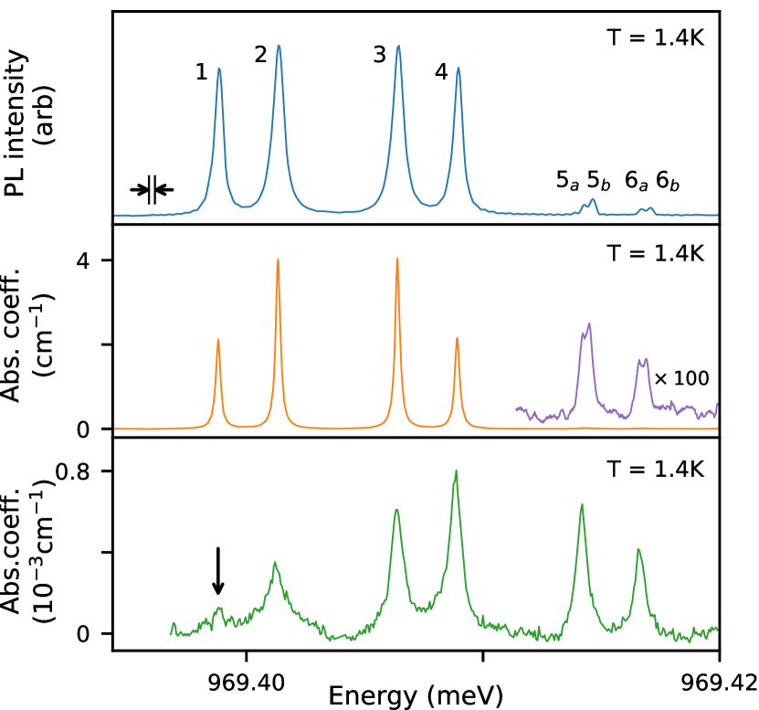
High resolution spectra of the G center NP line taken in both PL and absorption are shown in Fig. 2. The relative intensities of the components in the PL spectrum are strongly affected by reabsorption in the sample due to the remarkably strong G center absorption. Indeed, in the PL spectrum of the 320 kGy sample (data not shown), the peaks labelled 1 through 4 are seen as dips in an apparently broadened spectrum.
The relative intensities of the G center components can be accurately determined from the absorption spectra, even for the 320 kGy sample, where the absorption strengths were only approximately twice as large as in the 32 kGy sample, perhaps indicating that the creation of G centers at 320 kGy is limited by the availability of Cs in these 28Si samples. The absorption coefficients and integrated areas of the components are given in Table 2. While G center absorption spectra were collected using the FTIR for all samples, there was a small contribution of the instrumental linewidth to the observed linewidth even at the highest available resolution. As a result, the absorption spectra shown in Fig. 2 were collected using a scanning DFB laser with a linewidth much less than that of the G-line components. The linewidths of the G center components are reported in Table 1; they are a little over twice the homogeneous linewidth associated with a 5.9 ns lifetime Beaufils et al. (2018), indicating that nearly all the inhomogeneous broadening has been removed in 28Si, and revealing the G center as a near-homogeneous light emitter in the bulk.
| Abs. coeff. | Integrated area | |
|---|---|---|
| [cm-1] | [cm-2] | |
| G1 | 2.13 | 0.0060 |
| G2 | 4.02 | 0.0114 |
| G3 | 4.05 | 0.0117 |
| G4 | 2.17 | 0.0065 |
| G5a (13C) | 0.015 | 0.00004 |
| G5b (13C) | 0.021 | 0.00007 |
| G6a (13C) | 0.010 | 0.00003 |
| G6b (13C) | 0.013 | 0.00004 |
The G-line in 28Si is seen to have a symmetrical quartet structure which has been completely hidden within the inhomogeneous linewidth seen before in natSi. The relative intensities of the four components show within error a 1:2:2:1 ratio, and the pattern suggests transitions between two doublet levels with splittings of 2.5(2) eV and 7.5(2) eV, but we cannot at this time determine which of these splittings occurs in the ground state and which in the excited state, nor can we rule out transitions between singlet and quartet levels.
Also seen in Fig. 2 are weaker, higher-energy features labelled 5a, 5b, 6a and 6b, which we interpret as isotope-shifted versions of lines 3 and 4 for G centers which contain one 13C and one 12C instead of the predominant two 12C. The relative intensities of these components seen in the high resolution absorption spectrum are in reasonable agreement with the intensities to be expected from the 13C natural abundance ([ 13C]/[12C] = 0.0111). If this identification of 5a through 6b is correct, there must be 13C versions of lines 1 and 2 hidden under lines 3 and 4, as will be verified later. The a-b doublet structure of lines 5 and 6 may result from the inequivalence of the two C atoms in the G center.
Isotope shifts of the unresolved NP G-line in natSi due to one of the three isotopes of Si occupying the Sii site have been previously reported Thonke et al. (1981); Davies and do Carmo (1981) and are shown in the inset to the middle panel of Fig. 1. The 29Si and 30Si peaks are obviously absent from the enriched 28Si spectrum. An unresolved C isotope shift of 40 eV has been reported in comparing the relatively broad lines of natSi samples containing primarily 12C or a mixture of 12C and 13C Davies et al. (1983). The improved linewidths available in our 28Si spectra allow a much more precise measurement of the shifts due to one 13C, which for the a {b} component is 7.85(20) eV {8.1(2) eV}.
When measuring the G-line absorption spectrum using the scanning DFB laser a gradual bleaching of the absorption intensity was noted. The rapidity of this bleaching scaled with the DFB laser intensity incident on the sample, and the bleaching could be reversed by illuminating the sample with above-gap light at 1047 nm. This may indicate that resonant excitation of a G-line component can drive the transition from the optically-active B state to the optically-inactive A state Song et al. (1990), although the bleaching might also result from a change in charge state, or by populating a long-lived shelving state. The bleaching effect lasted at least 15 minutes with the sample not illuminated. On the ms to s time scales investigated here, pumping of either line 1, 2, 3 or 4 resulted in a simultaneous bleaching of all four main components.
Next we used this resonant bleaching effect to selectively reduce the intensity of the main 12C components to better reveal the spectrum of the isotope-shifted lines from centers having one 13C, as shown in the bottom panel of Fig. 2. An additional higher power DFB laser was set to the energy of component 1, as indicated by the arrow, while the absorption spectrum was collected with a scanning lower power DFB laser. No above-gap excitation was used during this scan. This resonant bleaching greatly reduced the strength of lines 1 through 4, revealing the 13C-shifted versions of lines 1 and 2 which are almost coincident in energy with the 12C lines 3 and 4. Under these conditions all lines were somewhat broader, and the a-b splittings could no longer be resolved.
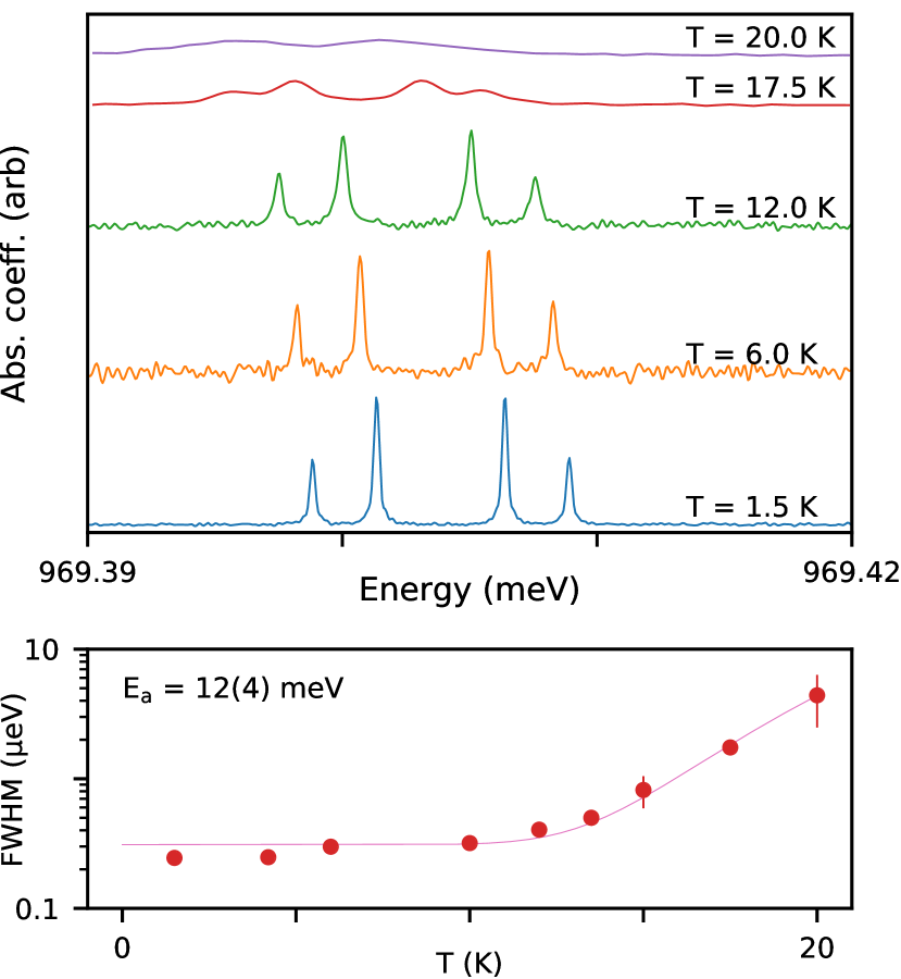
The temperature dependence of the full width at half-maximum (FWHM) of the main G-line components is shown in Fig. 3. The integrated absorption area of the combined G-line components was constant from 1.5 K to 20 K. Fitting the FWHM to a simple thermally-induced transitions model,
| (1) |
gave a thermal activation energy meV for this broadening, which may be evidence for an electronic excited state at that energy.
High resolution absorption spectra of the G-line components in 28Si were collected for applied magnetic fields up to 6 T, and no changes from the zero field spectra were observed. Given the greatly reduced linewidths seen in 28Si, this confirms and strengthens earlier conclusions that the G-line arises from a spin zero to spin zero transition Thonke et al. (1981).
III.2 C center (790 meV, 1571 nm)
The C center, with its NP line at 789.6 meV, is one of the most thoroughly studied radiation damage centers in Si (for an earlier review see section 5.1 in Davies (1989), and for more recent reviews see Pajot (2011) and Pajot and Clerjaud (2013)). It is known to have C1h symmetry and to contain one Ci and one Oi, and isotope shifts due to both C Davies et al. (1985); Kürner et al. (1989) and O Kürner et al. (1989) have been observed in spectra of the C center in natSi.
The electronic properties of the initial and final states of the C center are better understood than for the G and W centers. The C center is known to be a hole-attractive isoelectronic bound exciton (IBE), also known as a pseudodonor center, in which the hole is tightly bound by the defect potential, and an electron is Coulomb-bound to this positive charge Pajot (2011). The donor-like excited state spectrum of the C center has been observed using PLE spectroscopy Wagner et al. (1984). In the pseudodonor IBE model, the tight binding of the hole is thought to quench its angular momentum. The resulting pseudospin hole coupled to the spin electron leads to an exchange splitting of the IBE ground state into singlet and triplet states, with the triplet state lying below the singlet. Since transitions from the IBE triplet state to the defect ground state are partially forbidden, the triplet IBE state has a much longer radiative lifetime than the singlet, and can be difficult to observe.
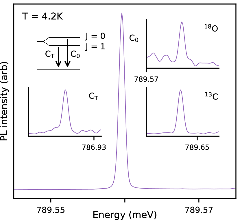
In a study of the transient decay of the C center PL, Bohnert et al. Bohnert et al. (1993) inferred that the observed NP C-line must originate from the singlet IBE state, and that there must be an unobserved triplet level lying 3.2 meV below the singlet level. This was confirmed later by the observation of PL from the triplet level (labelled CT) lying 2.64 meV below the singlet transition (now labelled C0) Ishikawa et al. (2009). Here we find a singlet-triplet splitting of 2.633 meV, in good agreement with the previously known result.
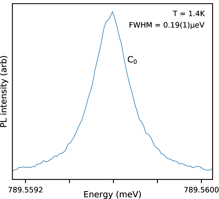
PL spectra collected with the FTIR of the main C0-line together with the CT-line and 18O and 13C isotope-shifted versions of the C0-line are shown in Fig. 4. We know that the linewidth of the C0-line was below the resolution limit of our FTIR, and there is no reason to believe that this was not also true of the CT line and the isotope-shifted lines. The true linewidth of the C0-line was determined by collecting a PLE spectrum using a scanning single frequency DFB diode laser, as shown in Fig. 5, and reported in Table 1. Unfortunately, the SNR was insufficient to observe any of the other C components in PLE.
Two isotope-shifted C0-lines are seen in Fig. 4, one lying at 789.6477 meV (also shown in Fig. 1) that has been observed previously in natural silicon and attributed to the C center with its 12C replaced by a 13C Kürner et al. (1989). We find an isotopic shift of E = 0.0881 meV, in good agreement with the previously published E = 0.089 meV value. We also observe a distinct isotopically shifted line due to 18O replacing 16O, with E = 0.0154 meV, which is reasonably close to the 0.024 meV shift previously observed in natSi samples with high 18O concentration Kürner et al. (1989). The much narrower linewidths available in 28Si make possible a more accurate determination of these isotope shifts without requiring samples doped with isotopically-enriched O or C.
III.3 W center (1018 meV, 1217 nm)
The W NP line is known to be an electric dipole transition at a trigonal center having spin-zero initial and final states, and showing only a Si isotope shift in its local vibrational mode replicas Davies et al. (1987b). It is currently thought to consist of three Sii Davies et al. (1987b, 2006); Surma et al. (2008), and shifted versions of the W-line have been observed in natSi implanted with different noble gas ions Bürger et al. (1984). The W center is thought to exist near more heavily damaged regions, and its linewidth in natSi is known to decrease with increasing annealing temperature Davies et al. (2006).
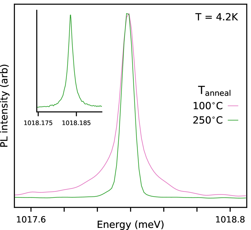
We observe this same behavior as shown in Fig. 6, where the superimposed low resolution PL scans show a much broader energy distribution for the sample annealed at 100 ∘C compared to the sample annealed at 250 ∘C. Note that the linewidth of the 250 ∘C sample shown in the main panel of Fig. 6 is strictly instrumental; a high resolution PL scan of the sample annealed at 250 ∘C is shown in the inset, and it is from this scan that the linewidth reported in Table 1 was obtained. Many weak, sharp lines were observed in the 100 ∘C annealed sample in the region immediately below the W-line, and while none of these agreed with known Bürger et al. (1984) noble-gas-shifted W-lines, they may be W centers shifted by the presence of other nearby defects which are annealed out at 250 ∘C. In agreement with earlier observations, and models for the W center composition, no isotope shifted W NP lines were observed in 28Si.
IV Conclusion
We have shown that the G, C and W radiation damage centers can readily be studied in highly-enriched, high-purity 28Si, even though the levels of C and O in the starting material are quite low. The inhomogeneous isotope broadening inherent to natSi can be eliminated in 28Si, resulting in linewidth improvements of over two order of magnitude for the C and G centers. Indeed, the linewidth of the G center components seen in 28Si are only slightly more than twice the limit imposed by homogeneous lifetime broadening, given the measured 5.9 ns G center lifetime Beaufils et al. (2018). The improved linewidths in 28Si allow for the clear observation of distinct isotope-shifted components which are much more difficult to observe in natSi. The spectrum of the G center in 28Si also reveals a quartet fine structure which is completely hidden in the inhomogeneously broadened spectrum in natSi. This fine structure may have applications in quantum technology, and certainly has implications for models of the G center structure and initial and final states. These results also have direct implications for the use of individual centers as single photon emitters even in natSi, since inhomogeneous isotope broadening will be absent for individual centers.
G, C and W are only a small subset of the known radiation damage centers in Si. The same linewidth improvements seen here for these centers in 28Si will apply to many other centers as well. The long list of known centers in silicon should be surveyed to look for possible applications in quantum technologies. In particular, it would be interesting to find a center which has an optically-resolved hyperfine splitting, since this could lead to an optically-accessible nuclear spin qubit, with the possibility of combining long coherence times with optical addressability, in a more accessible wavelength region than the proposed chalcogen spin/photon qubits which operate near 2900 nm Morse et al. (2017). The C center, with its convenient emission wavelength near 1550 nm and its potential transient access to a hyperfine-coupled nuclear spin via its excited state triplet, may provide a useful spin-photon interface.
Acknowledgements
This work was supported by the Natural Sciences and Engineering Research Council of Canada (NSERC), the Canada Research Chairs program (CRC), the Canada Foundation for Innovation (CFI), and the B.C. Knowledge Development Fund (BCKDF). The 28Si samples used in this study were prepared from the Avo28 crystal produced by the International Avogadro Coordination (IAC) Project (2004-2011) in cooperation among the BIPM, the INRIM (Italy), the IRMM (EU), the NMIA (Australia), the NMIJ (Japan), the NPL (UK), and the PTB (Germany). We thank Alex English of Iotron Industries for assistance with the electron irradiations.
References
- Davies (1989) G. Davies, “The optical properties of luminescence centres in silicon,” Physics Reports 176, 83–188 (1989).
- Shainline and Xu (2007) J.M. Shainline and J. Xu, “Silicon as an emissive optical medium,” Laser & Photonics Reviews 1, 334–348 (2007).
- Buckley et al. (2017) S. Buckley, J. Chiles, A. N. McCaughan, G. Moody, K. L. Silverman, M. J. Stevens, R. P. Mirin, S. Nam, and J. M. Shainline, “All-silicon light-emitting diodes waveguide-integrated with superconducting single-photon detectors,” Applied Physics Letters 111, 141101 (2017).
- Beaufils et al. (2018) C. Beaufils, W. Redjem, E. Rousseau, V. Jacques, A. Yu. Kuznetsov, C. Raynaud, C. Voisin, A. Benali, T. Herzig, S. Pezzagna, J. Meijer, M. Abbarchi, and G. Cassabois, “Optical properties of an ensemble of G-centers in silicon,” Phys. Rev. B 97, 035303 (2018).
- Karaiskaj et al. (2001) D. Karaiskaj, M. L. W. Thewalt, T. Ruf, M. Cardona, H.-J. Pohl, G. G. Deviatych, P. G. Sennikov, and H. Riemann, “Photoluminescence of isotopically purified silicon: How sharp are bound exciton transitions?” Phys. Rev. Lett. 86, 6010–6013 (2001).
- Cardona and Thewalt (2005) Manuel Cardona and M. L. W. Thewalt, “Isotope effects on the optical spectra of semiconductors,” Rev. Mod. Phys. 77, 1173–1224 (2005).
- Steger et al. (2009) M. Steger, A. Yang, M. L. W. Thewalt, M. Cardona, H. Riemann, N. V. Abrosimov, M. F. Churbanov, A. V. Gusev, A. D. Bulanov, I. D. Kovalev, A. K. Kaliteevskii, O. N. Godisov, P. Becker, H.-J. Pohl, E. E. Haller, and J. W. Ager, “High-resolution absorption spectroscopy of the deep impurities S and Se in revealing the hyperfine splitting,” Phys. Rev. B 80, 115204 (2009).
- Steger et al. (2012) M. Steger, K. Saeedi, M. L. W. Thewalt, J. J. L. Morton, H. Riemann, N. V. Abrosimov, P. Becker, and H.-J. Pohl, “Quantum information storage for over 180 s using donor spins in a 28Si “semiconductor vacuum”,” Science 336, 1280–1283 (2012).
- Morse et al. (2017) K. J. Morse, R. J. S. Abraham, A. DeAbreu, C. Bowness, T. S. Richards, H. Riemann, N. V. Abrosimov, P. Becker, H.J. Pohl, M. L. W. Thewalt, and S. Simmons, “A photonic platform for donor spin qubits in silicon,” Science Advances 3 (2017).
- Hayama et al. (2004a) S. Hayama, G. Davies, and K. M. Itoh, “Photoluminescence studies of implantation damage centers in 30Si,” Journal of Applied Physics 96, 1754–1756 (2004a).
- Hayama et al. (2004b) S. Hayama, G. Davies, J. Tan, J. Coutinho, R. Jones, and K. M. Itoh, “Lattice isotope effects on optical transitions in silicon,” Phys. Rev. B 70, 035202 (2004b).
- P. et al. (2009) Becker P., Pohl H.‐J., Riemann H., and Abrosimov N., “Enrichment of silicon for a better kilogram,” physica status solidi (a) 207, 49–66 (2009).
- Wagner et al. (1984) J. Wagner, K. Thonke, and R. Sauer, “Excitation spectroscopy on the 0.79-eV line defect in irradiated silicon,” Phys. Rev. B 29, 7051–7053 (1984).
- Davies et al. (1986) G. Davies, A. S. Oates, R. C. Newman, R. Woolley, E. C. Lightowlers, M. J. Binns, and J. G. Wilkes, “Carbon-related radiation damage centres in Czochralski silicon,” Journal of Physics C: Solid State Physics 19, 841 (1986).
- Davies et al. (1987a) G. Davies, E. C. Lightowlers, R. C. Newman, and A. S. Oates, “A model for radiation damage effects in carbon-doped crystalline silicon,” Semiconductor Science and Technology 2, 524 (1987a).
- Trombetta and Watkins (1987) J. M. Trombetta and G. D. Watkins, “Identification of an interstitial carbon-interstitial oxygen complex in silicon,” Applied Physics Letters 51, 1103–1105 (1987).
- Kürner et al. (1989) W. Kürner, R. Sauer, A. Dörnen, and K. Thonke, “Structure of the 0.767-ev oxygen-carbon luminescence defect in 450C thermally annealed Czochralski-grown silicon,” Phys. Rev. B 39, 13327–13337 (1989).
- Bohnert et al. (1993) G. Bohnert, K. Weronek, and A. Hangleiter, “Transient characteristics of isoelectronic bound excitons at hole-attractive defects in silicon: The C (0.79 eV), P (0.767 eV), and H (0.926 eV) lines,” Phys. Rev. B 48, 14973–14981 (1993).
- Canham et al. (1987) L. T. Canham, K. G. Barraclough, and D. J. Robbins, “1.3-m light-emitting diode from silicon electron irradiated at its damage threshold,” Applied Physics Letters 51, 1509–1511 (1987).
- Song et al. (1990) L. W. Song, X. D. Zhan, B. W. Benson, and G. D. Watkins, “Bistable interstitial-carbon–substitutional-carbon pair in silicon,” Phys. Rev. B 42, 5765–5783 (1990).
- Davies et al. (1987b) G. Davies, E. C. Lightowlers, and Z. E. Ciechanowska, “The 1018 meV (W or I1) vibronic band in silicon,” Journal of Physics C: Solid State Physics 20, 191 (1987b).
- Davies et al. (2006) G. Davies, S. Hayama, L. Murin, R. Krause-Rehberg, V. Bondarenko, A. Sengupta, C. Davia, and A. Karpenko, “Radiation damage in silicon exposed to high-energy protons,” Phys. Rev. B 73, 165202 (2006).
- Surma et al. (2008) B. Surma, P. Kaminski, A. Wnuk, and R. Kozlowski, “Some new photoluminescence features of W line for neutron-irradiated MCz-Si and FZ-Si,” 2008 IEEE Nuclear Science Symposium Conference Record (2008).
- Wang et al. (2014) H. Wang, A. Chroneos, C. A. Londos, E. N. Sgourou, and U. Schwingenschlögl, “G-centers in irradiated silicon revisited: A screened hybrid density functional theory approach,” Journal of Applied Physics 115, 183509 (2014).
- Timerkaeva et al. (2017) D. Timerkaeva, C. Attaccalite, G. Brenet, D. Caliste, and P. Pochet, “What is the nature of the C-C complex in silicon? Insights from electronic structure calculations,” ArXiv e-prints (2017), arXiv:1702.02334 .
- Cardona et al. (2004) M. Cardona, T. A. Meyer, and M. L. W. Thewalt, “Temperature dependence of the energy gap of semiconductors in the low-temperature limit,” Phys. Rev. Lett. 92, 196403 (2004).
- Thonke et al. (1981) K. Thonke, H. Klemisch, J. Weber, and R. Sauer, “New model of the irradiation-induced 0.97-eV () line in silicon: A complex,” Phys. Rev. B 24, 5874–5886 (1981).
- Davies and do Carmo (1981) G. Davies and M. C. do Carmo, “Isotope effects on the 969 meV vibronic band in silicon,” Journal of Physics C: Solid State Physics 14, L687 (1981).
- Davies et al. (1983) G. Davies, E. C. Lightowlers, and M. C. do Carmo, “Carbon-related vibronic bands in electron-irradiated silicon,” Journal of Physics C: Solid State Physics 16, 5503 (1983).
- Pajot (2011) B. Pajot, “Donor and donor-like EM spectra,” in Optical Absorption of Impurities and Defects in Semiconducting Crystal: Hydrogen-like Centres, Solid-State Sciences (Springer, Berlin, 2011) Chap. 6, pp. 169–280.
- Pajot and Clerjaud (2013) B. Pajot and B. Clerjaud, “Absorption of deep centres and bound excitons,” in Optical Absorption of Impurities and Defects in Semiconducting Crystal: Electronic Absorption of Deep Centres and Vibrational Spectra, Solid-State Sciences (Springer, Berlin, 2013) Chap. 4, pp. 113–188.
- Davies et al. (1985) G. Davies, E. C. Lightowlers, R. Woolley, R. C. Newman, and A. S. Oates, “Carbon, oxygen and silicon isotope effects in the optical spectra of electron-irradiated Czochralski silicon,” in Proc. 13th Internat. Conf. Defects Semicond., edited by L. C. Kimerling and J. M. Parsey, Jr. (The Metallurgical Society of AIME, New York, 1985) pp. 725–731.
- Ishikawa et al. (2009) T. Ishikawa, K. Koga, T. Itahashi, L.S. Vlasenko, and K.M. Itoh, “Photoluminescence from triplet states of isoelectronic bound excitons at interstitial carbon-intersititial oxygen defects in silicon,” Physica B: Condensed Matter 404, 4552 – 4554 (2009).
- Bürger et al. (1984) N. Bürger, K. Thonke, R. Sauer, and G. Pensl, “New class of related optical defects in silicon implanted with the noble gases He, Ne, Ar, Kr, and Xe,” Phys. Rev. Lett. 52, 1645–1648 (1984).