Fast and accurate functionalization of opaque conductive samples with single nano particles
Abstract
Single quantum emitters coupled to different plasmonic and photonic structures are key elements for integrated quantum technologies. In order to fully exploit these elements, e.g. for quantum enhanced sensors or quantum repeaters, a reliable fabrication method as enabling technology is crucial. In this work, we present a method that allows for positioning of individual nano crystals containing single quantum light sources on non-transparent conductive samples with sub-micrometer precision. We induce long-range electrostatic forces between an atomic force microscope (AFM) tip, which carries a nano particle, and the target surface. This allows for mapping of the target area in non contact mode. Then, the placement site can be identified with high accuracy without any tip approach, eliminating the risk of a particle loss. We demonstrate the strength of the method by transferring a diamond nano crystal containing a single nitrogen-vacancy defect to the center of a micrometer-sized silver bullseye antenna with nanometer resolution. Our approach provides a simple and reliable assembling technology for positioning single nano objects on opaque substrates with high reproducibility and precision.
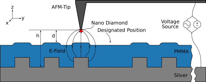
An ideal platform to study light-matter interaction at the fundamental level consists of single quantum emitters coupled to photonic and plasmonic elements Akimov et al. (2007); Wolters et al. (2010); Benson (2011); Andersen et al. (2018). Such elements are also needed to realize quantum interfaces between stationary and flying qubits operating with near unity efficiency Bernien et al. (2013). Reaching the required nanometer precision for optimum coupling is still a challenge. Approaches for different scenarios have been developed. Ion implantation in diamond nano structures was successful to create optically active defect centers at well defined locations Meijer et al. (2005, 2008); Sipahigil et al. (2016). In a complementary approach, first single emitters as quantum dots or defects in diamond nano crystals (nano diamonds) are identified and subsequently a structure is built around them Gschrey et al. (2013); Shi et al. (2016). In other cases emitters are spin-coated on masks exposing just the part of the sample that needs to be functionalized Bermúdez-Ureña et al. (2015); or the entire surface of a sample is covered with emitters and misplaced ones are etched away Harats et al. (2017). Another promising technique is the pick and place method. Here, single nano particles containing quantum emitters are transferred from substrate to substrate by employing an atomic force microscope (AFM) Schell et al. (2011) combined with a confocal scanning microscope (CSM). The method is highly accurate and deterministic and it also allows for pre-characterization of the luminescent particles. Moreover, the placement is not final, several iterations can be performed by nano manipulation if required. Unlike most other methods, neither a vacuum environment nor large and expensive electron beam lithography systems are required. However, the positioning precision relies on the fluorescence feedback observed via a CSM accessing the surfaces from below the substrate. Many important substrates for integrated quantum photonics, however, are opaque: dielectric waveguides and resonators are fabricated on silicon, plasmonic structures are based on metal films. In this case the pick and place method may still be applied Wolters et al. (2010); Andersen et al. (2018), but it is generally not possible to place the fluorescent nano crystal with sub-micrometer precision in a single shot. Here we present a fast and versatile technique allowing for high accuracy placement even on opaque structures. In order to demonstrate our method we chose a highly relevant architecture, i.e. a nano diamond containing a single nitrogen vacancy defect center (NV) coupled to a light collecting optical antenna. Such an element renders particularly useful as a quantum light source Shi et al. (2016), or for a fast read-out of the NV’s electron spin and thus faster and more efficient magnet field sensing Schirhagl et al. (2014). We use a Polymethylmethacrylate (PMMA) coated bullseye antenna Harats et al. (2017) whose cross section is schematically shown in Fig. 1 together with the conceptual idea of our approach. The antenna consists of a slab waveguide and concentrically arranged circular metal rings. The emitter couples to the slab waveguide that distributes the radiation over the metal grating. Each metal ring coherently scatters the emission, resulting in interference and a collimated light beam. A detailed discussion of the antenna’s working principle can be found in Ref. Abudayyeh and Rapaport (2017).

The functionalization approach starts with picking up a pre-characterized nano diamond of some ten nanometers in size hosting a single NV using a commercial AFM similar to what is described in Ref. Schell et al. (2011). In order to transfer the nano particle to a designated position on a structure on top of an opaque substrate with sub-micrometer precision requires knowledge of the structure’s topography. In principle this could be gained by scanning the AFM-tip across the substrate. However, with a functionalized tip carrying the nano particle, which is only attached by surface adhesion, this is impossible in regular AFM scanning modes because the particle would be detached too easily during scanning. Even the approach of the tip to the surface may lead to a loss of the nano diamond. To overcome this challenge, a non-contact approach and imaging principle must be used. In our method, we induce long range Coulomb interactions by applying a voltage between conductive tip and sample. This can be seen as a modified Kelvin Probe measurement, where the tip-surface distance is not kept constant Melitz et al. (2011).
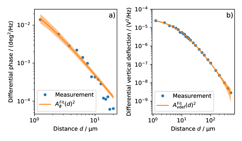
By applying the voltage, the mechanically driven tip experiences a force gradient along its direction of oscillation, which shifts the phase relative to the driving force and changes the oscillation amplitude at the same time. This changes in phase and oscillation amplitude depend on the distance between tip and surface, so that both can be used as a distance probe either to gain topology informations of the surface by recording height informations from a safe distance during scanning or to approach the surface without ever touching it, so that the just mentioned scans can be performed. The approach is performed while applying an AC voltage . This is necessary to compensate for drifts of the phase and oscillation amplitude while approaching, making it impossible to obtain voltage induced constant changes at distances . An analytical formula of the expected differential phase and amplitude change , , as well as a derivation of formulas and , which can be fitted to the acquired data, can be found in the supplementary material (Eq. S6 and S10). The latter are given by:
| (1) | ||||
| (2) |
with variable fit parameters , , , , and . The tip to surface distance can be measured directly by the AFM, while the equilibrium distance between tip and conductive surface is not directly accessible in this experiment. One should note that the square of the amplitudes must be fitted, since the power spectral density has been recorded. Those curves fit sufficiently to the experimental data, as can be seen in Fig. 2 a) and b), represented as solid curves. A mismatch between analytical formula and measured data is obtained for the differential phase at distances above due to the increased influence of the force between cantilever and surface at higher distances. Our model only takes into account the force between tip cone and surface, which dominates for distances below . In this region, the model matches the data so that it can be used as a calibration curve.

The fitted curves - once derived - then serve as quantitative calibration curves for the approach process. Further measurement runs show only minor deviations, which indicates for a reliable and robust technique. Even a change of the tip shape i.e. due to the picking process, has no major effect on the tip approach procedure. The vertical deflection signal is used to approach the tip starting at a distance of . At this large distance, no differential phase can be detected, because the signal scales with (see Eq. S5), whereas one term of the vertical deflection scales with (see Eq. S9). At the phase shift can be detected. Then it is preferably to use to approach the tip close and precise to the surface, as the signal change is higher than the vertical deflection signal.

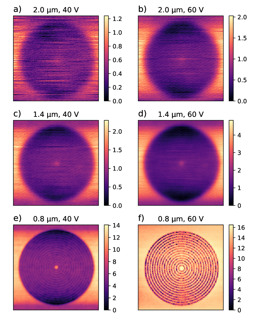
Once the non contact approach is done, a DC voltage is applied between tip and sample, which, as described above, causes a constant differential phase due to the occurrence of a force gradient. The distance dependent differential phase recorded during an xy-scan of the AFM tip at a fixed z-position maps the height of the metal surface. Fig. 3 shows these electrostatic force microscope images recorded at different voltages. Increasing the DC voltage at a constant distance increases the signal to noise ratio, as a higher phase change is detected. Lowering the tip to surface distance results in an increased xy-resolution, down to a sub-micron level, which determines the placement accuracy.

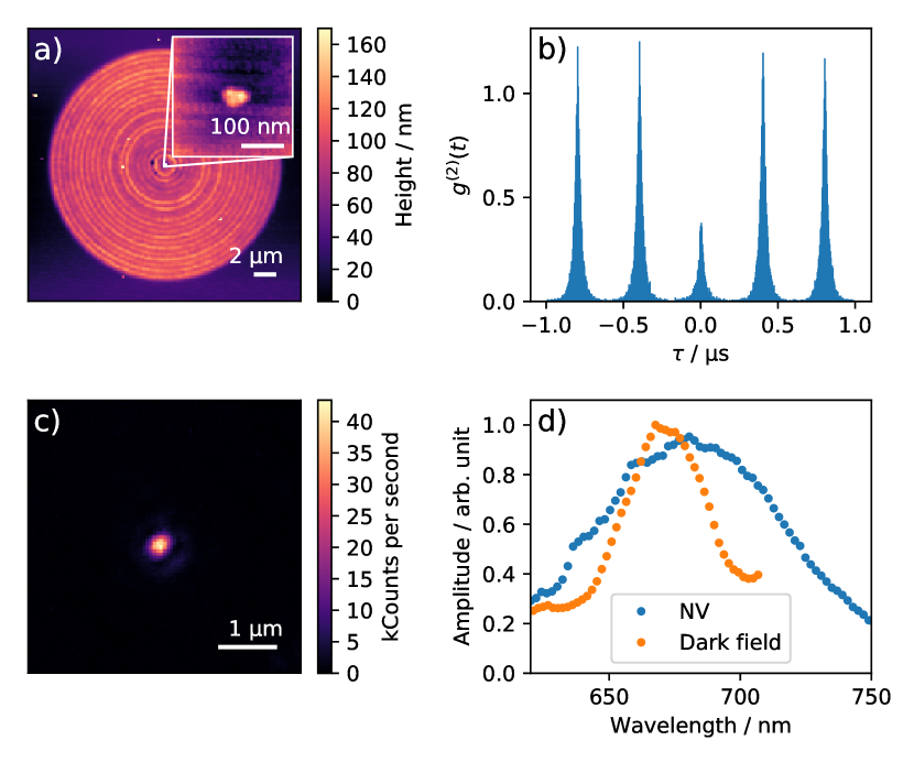
After switching off the voltage, the nano diamond is deposited by finally approaching the tip to the surface and applying a force similar to Ref. Schell et al. (2011). Subsequent nano manipulation reduces the deposition accuracy to the AFM resolution, which in this case correlates with the convolution of tip and diamond size. In this experiment we estimate the typical positioning accuracy to be below . In Fig. 4 a) an AFM-scan shows the final result, i.e. the successfully placed nano diamond in the center of a bullseye antenna. An optical confocal measurement of the same antenna reveals only a single diffraction limited spot (see Fig. 4 c). With a NA 0.9 objective lens, in saturation were detected. The excitation laser (Solea, PicoQuant) operated with a repetition rate of , at a central wavelength of , a wavelength span of and a CW power of . A -function taken from this fluorescence signal shown in Fig. 4 b) confirms the emission of non-classical light stemming predominately from a single emitter Schröder et al. (2011). This result nicely shows the operation of the antenna, i.e. efficient collection of photons, once the emitter is precisely positioned. A drawback of our chosen emitter, the NV center, is its broad emission spectrum extending from to (see fluorescence spectrum in Fig. 4 d). However, the bullseye antenna accounts for this by its broad optical response. In order to show this, we measured the dark field antenna spectrum, by collimating a light beam onto the antenna region. The direct reflection was filtered out and residual light stemming from the center was guided into the spectrometer. In this way, the inverse antenna operation was simulated. The resulting spectrum showed in d) fully overlaps with the NV fluorescence spectrum acquired from the positioned particle. Furthermore, the scattering efficiency profile indicates for potentially best collimation at . The measurements represent one example how our method of functionalization can be applied successfully to assemble an optimal structure for photon collection from NV centers in nano diamonds.
In summary, we presented a fast and versatile method that allows the deterministic placement of individual nano particles on opaque conductive substrates. After an initial tip-sample calibration, our method provides an effective and reproducible way to functionalize any kind of plasmonic or photonic structures realized on conductive surfaces, with a sub-micrometer precision limited only by the employed AFM.
This work was supported by the Einstein Foundation Berlin project ”ActiPlAnt” and the German Ministry of Education and Research (BMBF) project ”NANO-FILM”.
References
- Akimov et al. (2007) A. V. Akimov, A. Mukherjee, C. L. Yu, D. E. Chang, A. S. Zibrov, P. R. Hemmer, H. Park, and M. D. Lukin, Nature 450, 402 (2007).
- Wolters et al. (2010) J. Wolters, A. W. Schell, G. Kewes, N. Nüsse, M. Schoengen, H. Döscher, T. Hannappel, B. Löchel, M. Barth, and O. Benson, Applied Physics Letters 97, 141108 (2010).
- Benson (2011) O. Benson, Nature 480, 193 (2011).
- Andersen et al. (2018) S. K. H. Andersen, S. Bogdanov, O. Makarova, Y. Xuan, M. Y. Shalaginov, A. Boltasseva, S. I. Bozhevolnyi, and V. M. Shalaev, ACS Photonics , acsphotonics.7b01194 (2018).
- Bernien et al. (2013) H. Bernien, B. Hensen, W. Pfaff, G. Koolstra, M. S. Blok, L. Robledo, T. H. Taminiau, M. Markham, D. J. Twitchen, L. Childress, and R. Hanson, Nature 497, 86 (2013).
- Meijer et al. (2005) J. Meijer, B. Burchard, M. Domhan, C. Wittmann, T. Gaebel, I. Popa, F. Jelezko, and J. Wrachtrup, Applied Physics Letters 87, 261909 (2005).
- Meijer et al. (2008) J. Meijer, S. Pezzagna, T. Vogel, B. Burchard, H. Bukow, I. Rangelow, Y. Sarov, H. Wiggers, I. Plümel, F. Jelezko, J. Wrachtrup, F. Schmidt-Kaler, W. Schnitzler, and K. Singer, Applied Physics A 91, 567 (2008).
- Sipahigil et al. (2016) A. Sipahigil, R. E. Evans, D. D. Sukachev, M. J. Burek, J. Borregaard, M. K. Bhaskar, C. T. Nguyen, J. L. Pacheco, H. A. Atikian, C. Meuwly, R. M. Camacho, F. Jelezko, E. Bielejec, H. Park, M. Lončar, and M. D. Lukin, Science (New York, N.Y.) 354, 847 (2016).
- Gschrey et al. (2013) M. Gschrey, F. Gericke, A. Schüßler, R. Schmidt, J.-H. Schulze, T. Heindel, S. Rodt, A. Strittmatter, and S. Reitzenstein, Applied Physics Letters 102, 251113 (2013).
- Shi et al. (2016) Q. Shi, B. Sontheimer, N. Nikolay, A. W. Schell, J. Fischer, A. Naber, O. Benson, and M. Wegener, Scientific Reports 6, 31135 (2016).
- Bermúdez-Ureña et al. (2015) E. Bermúdez-Ureña, C. Gonzalez-Ballestero, M. Geiselmann, R. Marty, I. P. Radko, T. Holmgaard, Y. Alaverdyan, E. Moreno, F. J. García-Vidal, S. I. Bozhevolnyi, and R. Quidant, Nature Communications 6, 7883 (2015).
- Harats et al. (2017) M. G. Harats, N. Livneh, and R. Rapaport, Optical Materials Express 7, 834 (2017).
- Schell et al. (2011) A. W. Schell, G. Kewes, T. Schröder, J. Wolters, T. Aichele, and O. Benson, The Review of scientific instruments 82, 073709 (2011).
- Schirhagl et al. (2014) R. Schirhagl, K. Chang, M. Loretz, and C. L. Degen, Annual Review of Physical Chemistry 65, 83 (2014).
- Abudayyeh and Rapaport (2017) H. A. Abudayyeh and R. Rapaport, Quantum Sci. Technol 2 (2017).
- Melitz et al. (2011) W. Melitz, J. Shen, A. C. Kummel, and S. Lee, Surface Science Reports 66, 1 (2011).
- Schröder et al. (2011) T. Schröder, A. W. Schell, F. Gädeke, G. Kewes, T. Aichele, and O. Benson, in CLEO:2011 - Laser Applications to Photonic Applications (OSA, Washington, D.C., 2011) p. QFG1.