Study of wide-spectrum and high-resolution diffraction optical elements by stacks of binary phase gratings
I-Lin Ho1,∗, Wang-Yang Li1
1ChiMei Visual Technology Corporation, Tainan 741, Taiwan, R.O.C.
∗Corresponding author: sunta.ho@msa.hinet.net
Abstract
This work theoretically investigates wide-spectrum and high-resolution diffraction optical elements (DOE) that are made of stacks of low-resolution binary phase gratings, whereby the two-dimensional grids in different grating layers are arranged with specified displacements. We remodel the common Kinoform algorithm for this multi-scale architecture. Numerical computations show that, by increasing the number of stacking layers, the resolution of diffraction fields can be improved and that the stability of optical elements within broad spectrums is significantly enhanced. Practical concern on largely increasing the number of grating layers are efficiency of the optical designs in theory and the manufacture of stacks of ultra-thin grating films.
OCIS codes: 090.1760, 050.0050, 100.6640
1 Introduction
Modern day technology automation and advanced processing equipments for polymeric and composite materials have facilitated the production of more disciplinary and highly-creative products. The emergence of advanced coextrusion processing techniques especially allows for the fabrication of films composed of hundreds or thousands of multilayers with individual layer thicknesses down to a few tens of nanometers [1]. Using the unique characteristics of multilayered films has recently brought for diverse capabilities and new breakthroughs in material properties and multi-functional unitization. Examples include breathable films [2], optical gradient structures [3], shape memory polymers [4], micro- and nano-fibers [5], multilayer composites with brick-wall type microstructures [6], dual brightness enhancement film (DBEF) [7], etc. This present work mainly explores multilayer architectures for optical holography.
Through computer generated holography (CGH) [9], the field of optical holography has been used in many commercial applications, e.g. optical interconnection and diffraction optical elements (DOE) [10]. Kinoform [8] is one kind of phase hologram that manages wave fronts of an incident light by phase encoding, and can be operated with high diffraction efficiency. Many theoretical works also have reported on Kinoform optics under various approaches, e.g. simulated annealing method [11, 12, 13] and direct binary search method [14].
In this study, we apply multilayer architectures to study wide-spectrum and high-resolution Kinoforms, in case improving the physical characteristics of optical elements is not an easy-implemented option. Similar to superresolution imaging [15], the high-resolution diffraction optical element (Kinoform) is realized by displacement stacks of low-resolution binary phase gratings (see Fig. 1). Moreover, the displacement stack correlates the high-resolution wave-front profile of devices with low-resolution binary grids, and makes the definitions of phase (n=0,1,2…) distinguishable and deterministic during optimization processes. All these features are proved to significantly enhance the stability of performance of current Kinoform architectures on large variations of incident wavelengths.
To carry out numerical calculations, we remodel the common Kinoform algorithm [11] for the studied multi-scale architecture. Relevant codes by Matlab and Fortran-MEX can be downloaded online[16]. It is emphasized that, for optical elements with sub-wavelength resolutions, dominant interference effects should be considered in the optimization algorithms. Popular methods include the scalar diffraction model and effective medium model [17]. The present work only follows regular conditions for Kinoform. Another vector diffraction algorithm for phase holograms is preparing, which shall be reported for sub-wavelength optical devices in a future work.
2 Geometric arrangements and algorithms
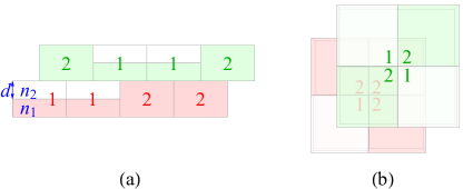
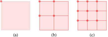
The optical elements presented herein are displacement stacks of optical layers with planar shifts at sub-grid accuracy. The optical layer is the binary phase grating that consists of two kinds of grids with optical path lengths: (i) and (ii) (see Fig. 1). Here, is the thickness of the optical layer, is the wavelength of the incident light, and defines the modulation phase of the binary grating. Figure 1(a) shows the stack of 2 binary grating layers with half-grid displacements from the side perspective, while Fig. 1(b) displays a double-resolution grid pattern from the top perspective. In this work, we adopt the arrangements of displacement stacks as Fig. 2, in order to extend to cases with arbitrarily high resolutions. Figure 2 shows the arrangements for original, double, and triple resolutions of diffraction images, corresponding to , , and shift positions, respectively. Despite the enhancement of the resolution, we note that the reconstruction of images operates on optimizing low-resolution grids in all binary gratings. This implies that the high-resolution wave-front profile of devices is not operated independently as in conventional models, but correlates with the low-resolution grids of binary gratings. To treat the optimization of this multi-scale architecture, we remodel the common Kinoform algorithm [11] here.
We denote the intensity profiles of the diffraction images by on coordinate (x,y), and the phase profiles of -binary grating by on coordinate . The high-resolution profile of the wave front of the optical element now is given by
| (1) | |||||
| (2) |
where the common factor has been omitted in Eq. (2), since the global phase shift will not change physical observations. The reconstructed diffraction images are . Here, is the inverse Fourier transform of . Following the iterative Fourier transform [11] processes, one can obtain optimized phase profiles for all binary layers. To score the optimization algorithm, an error function [11] is defined as the mean-square error between target image and reconstructed image :
| (3) | |||||
| (4) |
3 Numerical simulations
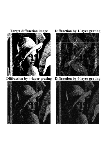
We first carry out digital simulations to investigate the performance of the present optical elements. The target diffraction image with 510510-pixels is depicted in the upper-left plot of Fig. 3. Binary phase gratings used in this work are set to have 170170-pixels (grids). The modulation phase of binary gratings is set to be in the single-binary-layer case and in multilayer cases. In the case for using single binary layer, the target image’s resolution is reduced to that of the binary layer by simulating responses of sensors using the majority decision method. Numerical computations for the single binary layer shows a result similar to that by the conventional method, featuring image symmetry with respect to the origin (see the upper-right plot of Fig. 3). This origin symmetry is intrinsic for single binary phase grating. Equation (5) below gives an analytical inference.
| (5) | |||||
Here, the condition for single binary phase grating, , is applied for the derivation of the last-line formula. From Eq. (5), one knows that the diffraction intensity is always the same with for the single-binary-layer case, obeying origin symmetry. For the double-resolution design, we adopt the arrangement in Fig. 2(b) to stack four binary layers. The resolution of the target image is correspondingly treated by simulating sensor responses. The computed diffraction image is depicted in the bottom-left plot of Fig. 3, which inherits properties of four-level phase gratings and shows outlines closed to the target plot. For the triple-resolution condition, we adopt the arrangement in Fig. 2(c) to stack nine binary gratings. The computed diffraction image, in the bottom-right plot of Fig. 3, presents almost the same details with the target image. It is concluded that the multilayer architecture can improve the resolution of diffraction images by optimizing low-resolution grid profiles in all displaced binary gratings.
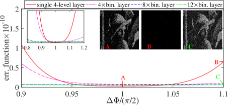
To investigate the performance of the optical element within broad spectrums, we study the deviations of diffraction images from the target one at different incident wavelengths. Here, the diffraction deviation is quantified by the error function in Eq. (3). The variable of incidence wavelengths is associated with the modulation phase by the equation , with . We analyze four kinds of optical elements: (i) conventional single 4-level(,,,) grating layer with 340340 pixels; (ii) stacking four binary gratings (170170 pixels/each), using the double-resolution scheme of Fig. 2(b); (iii) stacking eight binary gratings, two layers per position in the double-resolution scheme; and (iv) stacking twelve binary gratings, three layers per position in the double-resolution scheme.
The resolution of the target image is scaled as 340340 pixels to coincide with that of the four optical elements. It is noted that optical elements (i) and (ii) have maximal modulation phase as in conventional designs [11]. Optical elements (iii) and (iv), however, have maximal modulation phase and , respectively. In contrast with conventional applications [11], the definitions of phase (n=0,1,2,…) in the studied multilayer architectures are distinguishable and deterministic during optimization processes, since the displacement stack correlates the high-resolution wave-front profile with the low-resolution binary grids as in Eq. (1).
Numerical results about the relation of diffraction deviations and incident wavelengths are shown in Fig. 4. Here, the conventional 4-level grating [11] gives less diffraction deviation than others at the designed value (see point A on the red-solid curve and the corresponding inset image A). As is away from the designed value (), diffractions of the conventional grating significantly deviate from the target profile and feature an image with overwhelming central zero-order intensity (see point B on the red-solid curve and the corresponding inset image B). The 4binary-layer optical element presents variations of diffraction similar to that of the conventional case near the designed value, since it inherits properties of 4-level phase gratings.
We notice that there are three differences between the conventional grating and the 4binary-layer grating: (i) the performance of the conventional grating is better than that of the 4binary-layer grating on the designed condition ; (ii) the decline in performances of the 4binary-layer grating is less than that from conventional grating as is away from the designed condition; and (iii) deviations in performances of the 4binary-layer grating are obviously asymmetric in the case that is away from the designed condition in increasing and decreasing directions.
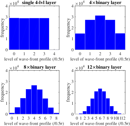
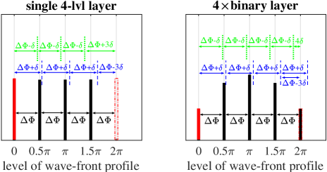
To understand these differences, we calculate histograms of phase levels of wave-front profiles for relevant optical elements in Fig. 5. The variations of levels of wave-front profiles with respect to increasing and decreasing are shown in Fig. 6, in which the solid bars in Fig. 6(a-b) redraw the histograms of wave-front profiles for the conventional grating and the 4binary-layer grating as in Fig. 5(a-b). The red-dot-dash bars in Fig. 6 represent the underlying/intrinsic modulation level owing to the -periodicity of phase.
We discuss some findings here:
(i) As indicated in Fig. 5(b-d), the optical elements by displacement stacks present Gaussian-type distributions on levels of wave-front profiles, in contrast with the uniform distribution for the conventional one in Fig. 5(a). This constraint about Gaussian-type distribution results from correlations between high-resolution wave-front pixels and low-resolution binary grids in the 4binary-layer grating, and reduces the degrees of freedom of the modulation phase during optimization processes. Consequently the performance of the conventional grating is better than that of the 4binary-layer grating on the optimized condition .
(ii) In Fig. 6(a), with increasing or decreasing , different phase intervals of wave-front levels do not equidistantly deviate for the conventional grating, especially the fourth interval (). The abrupt (fourth) modulation interval significantly disturbs the regularity of constructive and destructive interference as well as the management of wave fronts of the incident light. For the 4binary-layer grating, since the fifth modulation level () exists, different modulation intervals can equidistantly deviate with varying (see Fig. 6(b)). Hence, the performance of the 4binary-layer grating is better than that of the conventional grating at varying away from the designed condition.
(iii) In Fig. 6(b), the underlying/intrinsic level (red-dot-dash bar) at also participates in the phase modulation. This level particularly contributes to asymmetric modulation intervals and on increasing and decreasing , respectively. The asymmetry of these two modulation intervals implies distinct deviations of performances in the 4binary-layer grating when increasing and decreasing (see the purple-dot-dash curve in Fig. 4).
For the optical elements with 8 binary layers and 12 binary layers in Fig. 4, the performances are much stable under largely varying (, see the inset plot C in Fig. 4), or alternatively, within a broad incident spectrum. It is inferred that optical elements with numerous displacement stacking layers decrease the populations of side levels (see Fig. 5(c-d)) and irregular modulation intervals at varying incident wavelengths. Moreover, spatial interferences among nearby pixels in the wave-front mask will seldom cross large phase intervals, owing to the non-trivial pixel correlations. All these factors benefit stable performances of the present Kinoform architectures on large variations of incident wavelengths.
4 Conclusion
This work studies multilayer architectures for diffraction optical elements, and presents relevant optimization algorithms. Numerical computations show that high-resolution diffraction images can be realized by devices using displacement stacks of low-resolution binary phase gratings. In additions, with the number of binary layers up to , this element presents a much more stable optical performance on variations () of incident wavelengths.
5 Acknowledgement
This work was supported by ChiMei Visual Technology Corporation.
References
- [1] D. Langhe and M. Ponting, ”Manufacturing and Novel Applications of Multilayer Polymer Films”, New York: William Andrew, Elsevier (2016).
- [2] G.T. Offord, S.R. Armstrong, B.D. Freeman, E. Baer, A. Hiltner, and D.R. Paul, ”Gas transport in coextruded multilayered membranes with alternating dense and porous polymeric layers”, Polymer 55, 1259 (2014).
- [3] M. Ponting, T.M. Burt, L.T.J. Korley, J. Andrews, A. Hiltner, and E. Baer, ”Gradient Multilayer Films by Forced Assembly Coextrusion”, Ind. Eng. Chem. Res. 49, 12111 (2010).
- [4] J. Du, S.R. Armstrong, E. Baer, ”Co-extruded multilayer shape memory materials: Comparing layered and blend architectures”, Polymer 54, 5399 (2013).
- [5] J. Wang, D. Langhe, M. Ponting, G. Wnek, and L.T.J. Korley,”Manufacturing of polymer continuous nanofibers using a novel co-extrusion and multiplication technique”, Polymer 55, 673 (2014).
- [6] M. Gupta, Y. Linn, T. Deans, E. Baer, A. Hiltner, and D.A. Schiraldi, ”Structure and Gas Barrier Properties of Poly(propylene-graft-maleic anhydride)/Phosphate Glass Composites Prepared by Microlayer Coextrusion”, Macromolecules 43(9), 4230 (2010).
- [7] M.F. Weber, C.A. Stover, L.R. Gilbert, T.J. Nevitt, and A.J. Ouderkirk, ”Giant Birefringent Optics in Multilayer Polymer Mirrors”, Science 287, 2451 (2000).
- [8] L.P. Lesem, P.M. Hirsch, and J.A. Jordan, ”The Kinoform: A New Wavefront Reconstruction Device”, IBM J. Res. Dev. 13, 150 (1969).
- [9] W.H. Lee, ”Sampled Fourier Transform Hologram Generated by Computer”, Appl. Opt. 9, 639 (1970).
- [10] S.B. Odinokov and H.R. Sagatelyan, ”The Design and Manufacturing of Diffraction Optical Elements to form a Dot-Composed Etalon Image within the Optical Systems”, Optics and Photonics Journal 3, 102 (2013).
- [11] Y.W. Chen, S. Yamauchi, N. Wang, and Z. Nakao, ”A Fast Kinoform Optimization Algorithm Based on Simulated Annealing”, IEICE Trans. Fundamentals E83-A, 774 (2000).
- [12] N. Yoshikawa and T. Yatagai, ”Phase optimization of a kinoform by simulated annealing”, Appl. Opt. 33, 863 (1994).
- [13] J. Turunen, A. Vasara, and J. Westerholm, ”Kinoform phase relief synthesis: a stochastic method”, Opt. Eng. 28, 1162 (1989).
- [14] M.A. Seldowitz, J.P. Allebacha, and D.W. Sweeney, ”Synthesis of digital holograms by direct binary search”, Appl. Opt. 26, 2788 (1987).
- [15] M. Irani, and S. Peleg, ”Improving resolution by image registration”, CVGIP: Graphical Models and Image Processing 53, 231 (1991).
- [16] https://goo.gl/S2iB7y
- [17] D. Ruan, L. Zhu, X. Jing, Y. Tian, L. Wang, S. Jin, ”Validity of scalar diffraction theory and effective medium theory for analysis of a blazed grating microstructure at oblique incidence”, Appl Opt. 53(11), 2357 (2014).