Electrostatically induced phononic crystal
Abstract
The possibility of realizing an electrostatically induced phononic crystal is investigated numerically in an acoustic waveguide based on a graphene sheet that is suspended over periodically arrayed electrodes. The application of dc voltage to these electrodes exerts electrostatic force on the graphene and this results in the periodic formation of stress in the waveguide structure in a non-invasive way, unlike the cases with mass loading and air holes. This non-invasive scheme enables a bandgap, namely a , to be created in the waveguide that can be used to dynamically tune the acoustic transparency in the medium. Our approach will allow the dispersion relation to be locally modified, thus modulating the temporal response of traveling acoustic phonon waves. This novel phonon architecture is promising in terms of realizing the advanced control of phonon dynamics such as waveform and dissipation engineering in the device.
A phononic crystal (PnC) is a promising platform for tailoring the dispersion relation of acoustic phonon waves and engineering the transmission properties Narayanamurti et al. (1979); Martnez-Sala
et al. (1995); Maldovan (2013). Hence, the advent of this artificial phonon architecture has attracted considerable interest in phononics Liu et al. (2000); Benchabane et al. (2006); Mohammadi et al. (2009); Otsuka et al. (2013); Boechler et al. (2011); Laude et al. (2006). The aim in the field is to develop highly functional phononic devices such as signal processors Mohammadi and Adibi (2011) and ultrahigh- mechanical oscillators Tsaturyan et al. (2017), and also to open up possible applications in topological physics Mousavi et al. (2015); He et al. (2016); Brendel et al. (2018), thermal management Zen et al. (2014); Maire et al. (2017); Kodama et al. (2017) and electro-/opto-mechanics Mohammadi et al. (2010); Fang et al. (2016); Balram et al. (2016).
To further increase the functionality in these devices, intensive efforts have been devoted to developing dynamic PnCs that allow the temporal control of acoustic waves with an external stimulus. Most of these PnCs have been based on macroscale solid-fluid Caleap and Drinkwater (2013); Wang et al. (2017) or sonic crystals Casadei et al. (2012). In contrast, a chip-based PnC platform has recently been demonstrated that consists of a membrane resonator array with a GaAs/AlGaAs heterostructure Hatanaka
et al. (2014a). The ability to dynamically control acoustic waves by using the mechanical nonlinearity in the device has made it possible to realize functional acoustic devices Hatanaka
et al. (2014b); Hatanaka et al. (2017). However, these devices suffer from the low breakdown in the GaAs piezoelectric transduction and the narrow operation bandwidth. Additionally, in most conventional PnC devices, the formation of the bandgap still relies on their passive geometric structure, which also determines the fundamental limitation of the dynamic control.
One of the keys to overcoming these difficulties is to use an electromechanical resonator based on graphene Chen et al. (2009); Weber et al. (2014, 2016); Mathew et al. (2016); Alba et al. (2016) and other two-dimensional (2D) materials Morell et al. (2016). This is because these layered materials host a low mass and a large Young modulus ( 10-17 kg and = 1 TPa in graphene, respectively Weber et al. (2014)) that enhance the mode coupling nonlinearity of the resonator ( ) Eichler et al. (2012). Additionally, they have extremely low rigidity that enables them to be stretched significantly by employing modest electrostatic force. This deformation induces stress without any invasive physical contact and realizes large mechanical tunability. As a result, the electrically active phonon systems using graphene and other 2D materials have demonstrated a range of dynamic control over acoustic resonant vibrations including coherent manipulation between different modes Mathew et al. (2016); Alba et al. (2016) and the possibility to tune the operating frequency by a large amount Chen et al. (2009); Weber et al. (2014); Takamura et al. (2014); Weber et al. (2016); Mathew et al. (2016); Alba et al. (2016).
In this letter, we propose an electrostatically induced PnC based on graphene electromechanical resonators, and we investigate the properties using the finite element method (FEM). The application of a dc voltage to a gate electrode array underneath a suspended graphene waveguide (WG) exerts electrostatic force on the graphene, which induces bending toward the electrodes Chen et al. (2009); Weber et al. (2014, 2016); Mathew et al. (2016); Alba et al. (2016); Morell et al. (2016). This electrostatic stretching forms a periodic elastic potential in the WG and modulates the dispersion relation of traveling acoustic waves, enabling bandgaps to be non-invasively created. Consequently, this non-invasive approach can realize a dynamic transition in the acoustic conduction property from transparency to opacity, i.e. from WG to PnC. This also enables the temporal control of group velocity and the trapping of the acoustic waves in an arbitrary position. Thus, the graphene-based phonon architecture will open up possible applications in the fields of signal processing and electromechanics.
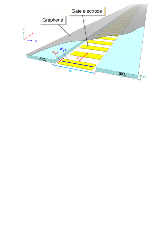
The device consists of a graphene multilayer with a thickness = 8.5 nm ( is the thickness of graphene monolayer, 0.34 nm) and density 2235 kg/m3 ( is a correction factor for contamination on a graphene surface, 4.5 used in this study Weber et al. (2014)). The graphene sheet is suspended over a rectangular trench of length and width 3.2 m ( ) fabricated from an insulating material such as SiO2 as shown in Fig. 1. A gate electrode with the dimensions (, ) = (1.60 m, 2.88 m) is periodically arrayed with a pitch of 3.2 m at the bottom of the trench and the electrodes are spatially separated in vacuum from the suspended graphene by a distance 85 nm 170 nm. The geometric parameters used in this study are typical values taken from previous experimental studies on individual mechanical resonators Weber et al. (2014, 2016).
Electrostatic pressure can be induced by applying a dc electric voltage to the gate electrodes and it reads
| (1) |
where , and are the capacitance per unit area formed between the graphene and the gate electrode, vacuum permittivity and the static displacement of the graphene induced by the electrostatic force, respectively. The electromechanical properties and dispersion relation are simulated in the unit structure of the WG with COMSOL Multiphysics. It should be noted that in the simulation, the graphene unit structure is given fixed boundary and Floquet periodic conditions at (, ) = (, /2) and (/2, ), respectively. Here, is the separation between the electrodes on which we apply the gate voltage. The electrodes that are not voltage biased are left connected to ground.
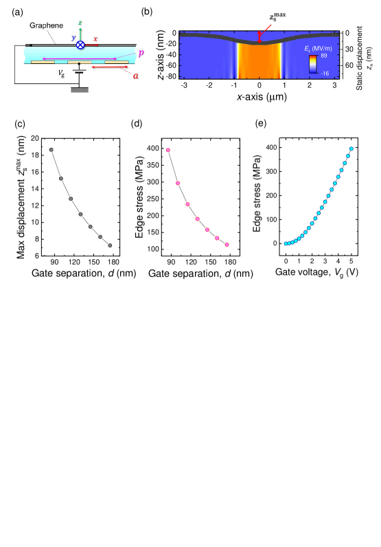
To understand the static electromechanical property of the device, we consider a unit structure with two electrodes in unit length and investigate the mechanical deformation of the graphene when we apply a gate voltage to one of the two electrodes as shown in Fig. 2(a). The application of the gate voltage concentrates the electric field between the graphene and the electrode, which exerts an electrostatic force on the graphene and thus bending it toward the electrode as shown by the solid grey line in Fig. 2(b). The static displacement gets larger when decreasing gate separation as shown in Fig. 2(c). The largest displacement of the graphene along the trench axis is between 18.6 and 7.2 nm for between 85 and 175 nm. Such large deformations cannot be achieved with conventional mechanical devices. This deformation induces large stress in the suspended graphene WG, which increases to 395 MPa at the edges when = 85 nm as shown in Fig. 2(d), and this value can also be adjusted by changing the gate voltage as shown in Fig. 2(e). These results reveal that the electrostatic graphene WG devices enable the generation of periodic stress and elastic potential variations in a non-invasive way, in contrast to previous works where stress was induced by loading mass and making air holes Martnez-Sala
et al. (1995); Maldovan (2013).
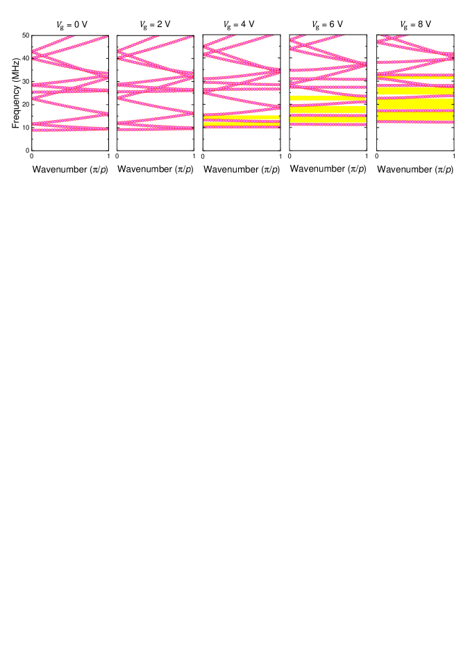
The emergence of the phononic bandgap results from the Bragg reflection of acoustic waves traveling in the periodic elastic potential. In the following, we investigate the electrostatic effect on the band dispersion in the WG. Figure 3 shows the dispersion relation in the device at various gate voltages. It exhibits parabolic dispersion curves at small gate voltages = 0 V and 2V as shown in the first and second panels from the left in Fig. 3, respectively, which are a trivial property of a normal WG structure. However, an increase in the gate voltage to 4 V results in a sizeable effect of the electrostatically induced periodic stress on the dispersion curve with the formation of bandgaps as shown in the middle panel of Fig. 3. By further increasing the gate voltage to = 6 V and 8 V, the spectral width of the bandgaps is broadened and the dispersion curves become flattened as shown in the second and first panels from the right in Fig. 3, respectively. Our approach can be used to dynamically manipulate the band structure and thus the acoustic wave during propagation.
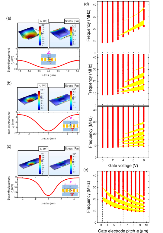
Most importantly, another advantage of this scheme is to modify the periodic pitch of the elastic potential by simply changing the configuration of the applied gate voltage. We here modify the periodic pitch between , and (Fig. 4(a)-(c)). This engineering of the gate voltage configuration alters the periodic elastic potential and thus enables the dispersion relation to be reconfigured. With , the gate electrode separation is short and this causes quasi-uniform deformation of the graphene sheet along the -axis so that the entire WG is stretched towards the electrodes. Thus the induced stress is not strongly localized but distributed throughout the entire device as shown in Fig. 4(a). Therefore, few bandgaps emerge. On the other hand, the cut-off frequency increases greatly when increasing gate voltage due to the uniform stress as shown in the top panel of Fig. 4(d). By changing the periodic pitch to and , the gate-induced deformation and stress are being localized as shown in Fig. 4(b) and (c), respectively. As a result, multiple bandgaps occur, and the cut-off frequencies are less dependent on the gate voltage, as shown in the middle and bottom panels of Fig. 4(d), respectively.
Changing the gate electrode pitch also modifies the bandgaps as shown in Fig. 4(e), where we used and V. This clearly indicates that the spectral position of the bandgaps varies and the number of sizerable bandgaps increases when increasing pitch . In particular, when 3.2, 6.4 and 9.6 m (dashed lines), the same gate configurations as in Figs. 4(a), 4(b) and 4(c) are realized, respectively. In this way, the electrostatic force induced by the gate electrode array allows the band dispersion in the WG to be designed with the gate voltage configuration.
For the experimental realization of a bandgap in the PnC, it would be necessary to prepare a WG with a length longer than 100 Hatanaka
et al. (2014a). This would correspond to between 0.32 mm and 0.96 mm in our model. Such millimeter-scale graphene can be obtained by chemical vapor deposition. The large graphene sample can be suspended by the usual dry-transfer method Castellanos-Comez
et al. (2014) and the recently developed vacuum stack process Kang et al. (2017). Although the stress that is built in during fabrication might be nonuniform along the WG, this can be compensated for by applying the appropriate to each gate electrode. Thus, we expect that graphene-based PnCs can be realized with existing fabrication techniques.
This novel PnC layout offers several advantageous features when compared to the conventional PnC devices. First, the PnC band structure is created by the electrostatic force induced by the spatially isolated electrodes. Therefore, this non-invasive approach enables on-demand tuning of the acoustic transparency of the device. Second, the gate voltage configuration determines the band structure. This not only modulates the spectral positions of the bandgaps, but it can also create a defect cavity at any desired location via local voltage modification. For instance, this can allow the strain distribution at the clamping points to be tailored in the cavity by optimizing the gate voltages, which might be used to realize a -tunable mechanical resonator Tsaturyan et al. (2017). Finally, the electrostatic force can also modify the mechanical nonlinearity of the device, which tunes and enhances the nonlinear parametric effect Eichler et al. (2012). The ability to adjust both the nonlinearity and the dispersion of the device can be useful for investigating nonlinear phenomena such as phononic solitons. This is because the soliton is generated as a result of the balance between the effects of nonlinear phase modulation and group velocity dispersion on a traveling wave Kurosu et al. (2018). The control of both effects holds promise for the demonstration of the dynamic manipulation of the temporal and spectral waveforms of the acoustic wave.
In conclusion, we have proposed a new PnC structure where the periodic stress profile can be non-invasively induced in a suspended graphene WG by applying a dc voltage to a gate electrode array. As a result the dispersion relation is modulated and bandgaps are generated. Moreover, the spectral position and width of the bandgaps can be controlled by varying the periodic arrangement of the gate voltage application. The ability to dynamically engineer the band structures opens up the possibility of developing various acoustic devices for signal processing applications, and the approach can be also used to study novel nonlinear phononic phenomena and topological physics, and to construct highly functional electromechanical circuits.
This work was supported by a MEXT Grant-in-Aid for Scientific Research on Innovative Areas “Science of hybrid quantum systems” (Grant No. JP15H05869 and JP15K21727), the Foundation Cellex, the CERCA Programme, AGAUR, Severo Ochoa (SEV-2015-0522), the grant FIS2015-69831-P of MINECO, and the Fondo Europeo de Desarrollo Regional (FEDER).
References
- Narayanamurti et al. (1979) V. Narayanamurti, H. L. Strmer, M. A. Chin, A. C. Gossard, and W. Wiegmann, Phys. Rev. Lett. 43, 2012 (1979).
- Martnez-Sala et al. (1995) R. Martnez-Sala, J. Sancho, J. V. Snchez, V. Gmez, and J. Llinares, Nature 378, 241 (1995).
- Maldovan (2013) M. Maldovan, Nature 503, 209 (2013).
- Liu et al. (2000) Z. Liu, X. Zhang, Y. Mao, Y. Y. Zhu, Z. Yang, C. T. Chan, and P. Sheng, Science 289, 1734 (2000).
- Benchabane et al. (2006) S. Benchabane, A. Khelif, J.-Y. Rauch, L. Robert, and V. Laude, Phys. Rev. E 73, 065601 (2006).
- Mohammadi et al. (2009) S. Mohammadi, A. A. Eftekhar, W. D. Hunt, and A. Adibi, Appl. Phys. Lett. 94, 051906 (2009).
- Otsuka et al. (2013) P. H. Otsuka, K. Nanri, O. Matsuda, M. Tomoda, D. M. Profunser, I. A. Veres, S. Danworaphong, A. Khelif, S. Benchabane, V. Laude, et al., Sci. Rep. 3, 3351 (2013).
- Boechler et al. (2011) N. Boechler, G. Theocharis, and C. Daraio, Nat. Mater. 10, 665 (2011).
- Laude et al. (2006) V. Laude, L. Robert, W. Daniau, A. Khelif, and S. Ballandras, Appl. Phys. Lett. 89, 083515 (2006).
- Mohammadi and Adibi (2011) S. Mohammadi and A. Adibi, AIP Adv. 1, 041903 (2011).
- Tsaturyan et al. (2017) Y. Tsaturyan, A. Barg, E. S. Polzik, and A. Schliesser, Nat. Nanotechnol. 12, 776 (2017).
- Mousavi et al. (2015) S. H. Mousavi, A. B. Khanikaev, and Z. Wang, Nature Commun. 6, 8682 (2015).
- He et al. (2016) C. He, X. Ni, H. Ge, X.-C. Sun, M.-H. L. Yan-Bin Chen, X.-P. Liu, and Y.-F. Chen, Nat. Phys. 12, 1124 (2016).
- Brendel et al. (2018) C. Brendel, V. Peano, O. Painter, and F. Marquardt, Phys. Rev. B 97, 020102 (2018).
- Zen et al. (2014) N. Zen, T. A. Puurtinen, T. J. Isotalo, S. Chaudhuri, and I. J. Maasilta, Nat. Commun. 5, 3435 (2014).
- Maire et al. (2017) J. Maire, R. Anufriev, R. Yanagisawa, A. Ramiere, S. Volz, and M. Nomura, Sci. Adv. 3, e1700027 (2017).
- Kodama et al. (2017) T. Kodama, M. Ohnishi, W. Park, T. Shiga, J. Park, T. Shimada, H. Shinohara, J. Shioki, and K. E. Goodson, Nat. Nanotechnol. 16, 892 (2017).
- Mohammadi et al. (2010) S. Mohammadi, A. A. Eftekhar, A. Khelif, and A. Adibi, Opt. Exp. 18, 9164 (2010).
- Fang et al. (2016) K. Fang, M. H. Matheny, X. Luan, and O. Painter, Nat. Photon. 10, 489 (2016).
- Balram et al. (2016) K. C. Balram, M. I. Davanco, J. D. Song, and K. Srinivasan, Nat. Photon. 10, 346 (2016).
- Caleap and Drinkwater (2013) M. Caleap and B. W. Drinkwater, PNAS 111, 6226 (2013).
- Wang et al. (2017) Y.-F. Wang, T.-T. Wang, Y.-S. Wang, and V. Laude, Phys. Rev. Appl. 8, 014006 (2017).
- Casadei et al. (2012) F. Casadei, T. Delpero, A. Bergamini, P. Ermanni, and M. Ruzzene, J. Appl. Phys. 112, 064902 (2012).
- Hatanaka et al. (2014a) D. Hatanaka, I. Mahboob, K. Onomitsu, and H. Yamaguchi, Nature Nanotech. 9, 520 (2014a).
- Hatanaka et al. (2014b) D. Hatanaka, I. Mahboob, K. Onomitsu, and H. Yamaguchi, Appl. Phys. Exp. 7, 125201 (2014b).
- Hatanaka et al. (2017) D. Hatanaka, T. Darras, I. Mahboob, K. Onomitsu, and H. Yamaguchi, Sci. Rep. 7, 12745 (2017).
- Chen et al. (2009) C. Chen, S. Rosenblatt, K. I. Bolotin, W. Kalb, P. Kim, I. Kymissis, H. L. Stormer, T. F. Heinz, and J. Hone, Nat. Nanotechnol. 4, 861 (2009).
- Weber et al. (2014) P. Weber, J. Gttinger, I. Tsioutsios, D. E. Chang, and A. Bachtold, Nano Lett. 14, 2854 (2014).
- Weber et al. (2016) P. Weber, J. Gttinger, A. Noury, J. Vergara-Cruz, and A. Bachtold, Nat. Commun. 7, 12496 (2016).
- Mathew et al. (2016) J. P. Mathew, R. N. Patel, A. Borah, R. Vijay, and M. M. Deshmukh, Nat. Nanotechnol. 11, 747 (2016).
- Alba et al. (2016) R. D. Alba, F. Massel, I. R. Storch, T. S. Abhilash, A. Hui, P. L. McEuen, H. G. Craighead, and J. M. Parpia, Nat. Nanotechnol. 11, 741 (2016).
- Morell et al. (2016) N. Morell, A. Reserbat-Plantey, I. Tsioutsios, K. G. Schdler, F. Dubin, F. H. L. Koppens, and A. Bachtold, Nano Lett. 16, 5102 (2016).
- Eichler et al. (2012) A. Eichler, M. del lamo Ruiz, J. A. Plaza, and A. Bachtold, Phys. Rev. Lett. 109, 025503 (2012).
- Takamura et al. (2014) M. Takamura, H. Okamoto, K. Furukawa, H. Yamaguchi, and H. Hibino, J. Appl. Phys. 116, 064304 (2014).
- Castellanos-Comez et al. (2014) A. Castellanos-Comez, M. Buscema, R. Molenaar, V. Singh, L. Janssen, H. S. J. van der Zant, and G. A. Steel, 2D Materials 1, 011002 (2014).
- Kang et al. (2017) K. Kang, K.-H. Lee, Y. Han, H. Gao, S. Xie, D. A. Muller, and J. Park, Nature 550, 229 (2017).
- Kurosu et al. (2018) M. Kurosu, D. Hatanaka, K. Onomitsu, and H. Yamaguchi, Nat. Commun. 9, 1331 (2018).