17,000 %/W Second-Harmonic Conversion Efficiency in Single-Crystalline Aluminum Nitride Microresonators
Abstract
High quality factor optical microcavities have been employed in a variety of material systems to enhance nonlinear optical interactions. While single-crystalline aluminum nitride microresonators have recently emerged as a low loss platform for integrated nonlinear optics such as four wave mixing and Raman lasing, few studies have investigated this material for second-harmonic generation. In this Letter, we demonstrate an optimized fabrication of dually-resonant phase-matched ring resonators from epitaxial aluminum nitride thin films. An unprecendented second-harmonic generation efficiency of 17,000%/W is obtained in the low power regime and pump depletion is observed at a relatively low input power of 3.5 mW. This poses epitaxial aluminum nitride as the highest efficiency second-harmonic generator among current integrated platforms.
On-chip optical nonlinearity has gained a significant interest for their applications in classical and quantum photonic information processing. Compared to their bulk counterparts, the tight optical confinement and facile device engineering in nanophotonic waveguides allow for greater experimental control over common nonlinear processes such as second-harmonic generation (SHG) (Cazzanelli et al., 2011; Chang et al., 2016; Fürst et al., 2010; Gromovyi et al., 2017; Guo et al., 2016a; Lin et al., 2016a; Wang et al., 2017; Wolf et al., 2017; Xiong et al., 2011; Roland et al., 2016), third harmonic generation (THG) (Surya et al., 2018; Levy et al., 2011; Wang et al., 2016), and photon-pair generation (Luo et al., 2017; Clemmen et al., 2009; Guo et al., 2016b; Sharping et al., 2006; Jin et al., 2014). These various nonlinear processes can be further combined, leading to applications of broadening the span of frequency combs (Guo et al., 2017; Lin et al., 2016b; Xue et al., 2017; Kowligy et al., 2018), f-2f referencing (Hickstein et al., 2017), and all-optical control of energy transfer between optical modes (Guo et al., 2018). Optical ring resonators have become a common modality to enhance the nonlinear effects. To date, various integrated platforms such as lithium niobate (Luo et al., 2017; Wang et al., 2014, 2017; Jin et al., 2014; Chang et al., 2016; Wolf et al., 2017; Lin et al., 2016b), silicon nitride (SiN) (Ning et al., 2012a; Levy et al., 2011; Ning et al., 2012b; Wang et al., 2016; Xue et al., 2017), gallium nitride (GaN) (Xiong et al., 2011; Gromovyi et al., 2017; Roland et al., 2016), and aluminum nitride (AlN) (Guo et al., 2016a, 2017; Pernice et al., 2012) have been employed to enhance the SHG efficiency beyond those seen in bulk crystals. AlN is particularly attractive for SHG for its large material band gap of 6.2 eV and mature fabrication processing. Polycrystalline AlN microring resonators (Guo et al., 2016a) have previously demonstrated state-of-the-art on-chip SHG conversion efficiency of 2500 %/W (0.025 mW-1), owing to careful engineering of the phase-matching between the infrared and visible modes as well as efficient waveguide coupling for both pump and SHG light. However, the efficiency of this device was ultimately limited by the intrinsic optical quality (Q) factor at both infrared (IR) and visible wavelengths. Increasing the material quality will ultimately reduce the optical loss at both fundamental and SHG wavelengths, allowing new record SHG efficiency.
Single-crystalline AlN has emerged as the likely successor to polycrystalline AlN photonics. As noted in previous studies, AlN epitaxially grown on sapphire substrates exhibit exceptionally high film quality and can achieve optical Q factors on the order of in the telecom band (Liu et al., 2017a), much higher than those typically observed in polycrystalline AlN (Guo et al., 2016a; Surya et al., 2018). Currently, AlN-on-sapphire devices have been employed for linear and nonlinear phenomena at telecom IR wavelengths (Liu et al., 2017b, 2018, 2016) as well as in the ultraviolet and visible regimes (Lu et al., 2018; Liu et al., 2017c). Recently demonstrated UV SHG (Fanto et al., 2016; Troha et al., 2016) in AlN-on-sapphire devices was only observable using a pulsed pump while visible SHG in this platform (Liu et al., 2017c) realized a low conversion efficiency due to the phase-mismatched condition. Lithography and etching challenges in processing thick (> 1 μm) AlN-on-sapphire films have proven as a barrier to achieving a fully-etched AlN waveguide (Liu et al., 2016, 2017b, 2017a, 2018), which is necessary to confine the phase-matched higher-order visible modes within the ring resonators.
In this Letter, we demonstrate a fabrication process for realizing fully-etched AlN-on-sapphire devices with a 1.1 μm thickness. This process is then employed to fabricate ring resonators with both high optical Q factors as well as a tunable phase-matching bandwidth of 1480-1640 nm. By optimizing the visible extraction waveguide and the coupling conditions of both infrared and visible modes, an on-chip SHG conversion efficiency of 17000 %/W was achieved in the low-power regime and a value of pm/V is extracted for epitaxial AlN. Pump depletion was observed in the high-power regime, with an absolute conversion efficiency as high as 11%.
We model the SHG process in a microring cavity possessing both an infrared and visible mode at angular frequencies and , respectively, each with internal loss rate, and external coupling rate . The coupling strength between these two resonance modes is represented by the parameter , which can be determined from the mode overlap between infrared and visible modes, the microring geometry, and the coefficient of AlN (Guo et al., 2016a). When pumping at a certain angular frequency, , SHG efficiency in the non-depletion regime can be expressed in terms of these cavity coupling rates as well as the detuning between the infrared (visible) resonances from the pump, , as
| (1) |
where and represent the on-chip SHG and pump power, respectively, and is the total coupling rate . Under ideal phase matching conditions, the microring geometry is optimized such that and . Fulfilling this dual-resonance condition, the SHG conversion efficiency can be reduced to
| (2) |
According to Eq. 2, maximum can be achieved when both the IR and visible modes are critically coupled () and the SHG efficiency is dependent only on the intrinsic device parameters. As noted in our previous report in polycrystalline AlN (Guo et al., 2016a), it is practically difficult to simultaneously achieve critical coupling for both modes in the phase-matched geometry and the maximum conversion efficiency is often limited by the cavity coupling rate.
In this experiment, single-crystalline AlN films are grown on c-plane sapphire by metal-organic vapor deposition (MOCVD) to a nominal thickness of 1.1 μm. The AlN-on-sapphire platform is quite insulating compared to typical silicon-based substrates and suffers from significant charging effects in our 100 kV electron-beam lithography process (Raith EBPG 5000+). While metal masks are typically used for increasing the conductivity of insulating substrates, many are not compatible with typical negative-tone resists such as hydrogen silsesquioxane (HSQ) and/or require a two-step etching process that ultimately limits the process selectivity (Liu et al., 2017a). To mitigate charging effects, we first spin a conventional FOx-16 HSQ mask followed by 300 nm poly(4-styrenesulfonic acid) (PSSA) before sputtering 10 nm gold. PSSA acts as a water-soluble sacrificial layer between the conductive gold layer and FOx-16 resist, allowing sufficient charge transfer to the HSQ layer and is easily removed during the development process (Rooks, ). Patterns are then developed in a 25% TMAH solution to maintain a high contrast. The patterns are then transferred to the AlN via an optimized Cl2/BCl3/Ar inductively coupled plasma (ICP) etch with a selectivity of 2.7:1 between AlN and FOx-16. Devices are then encapsulated in 1.0 μm plasma-enhanced chemical vapor deposition (PECVD) SiO2 and cleaved prior to measurement.
This process provides a simplified route for AlN-on-sapphire fabrication, requiring a single masking step compared to the two-step processes previously reported in Ref. (Liu et al., 2017a). The thicker FOx-16 mask and the high etching selectivity allow up to 1.4 μm of AlN to be fully etched, compared to 1.0 μm demonstrated previously. This fully etched structure is particularly important for tight confinement of the visible mode. Finite element method simulations indicate that the second-harmonic mode exhibits 1.2 dB/cm radiation loss when leaving a 200 nm unetched AlN layer (radius = 30um, height = 1 μm, width = 1.2 μm), whereas the radiation loss is negligible in the fully-etched structure.
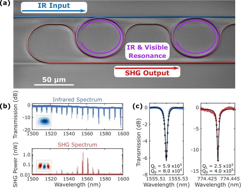
Fig. 1(a) depicts the final fabricated devices, where a 900 nm-wide bus waveguide is coupled to a microring resonator with a waveguide width of 1.2-1.3 μm. A thinner waveguide wrapped around the ring is employed to efficiently extract the near-visible light from the phase-matched ring resonator. The near-visible extraction waveguide width is tapered from 175 to 125 nm at a constant coupling gap. As a result, the fundamental mode of the extraction waveguide can be sufficiently matched to the near-visible ring mode while minimally perturbing the infrared ring mode. Seven ring resonators share the same IR bus and visible drop waveguides to account for fabrication imperfections across the AlN chip. The infrared and visible waveguides rejoin in an on-chip wavelength division multiplexer (WDM), while an off-chip WDM separates the infrared and near-visible light for simultaneous characterization (Guo et al., 2016a, c, 2017).
Microring resonances are observed by sweeping the wavelength of an infrared external cavity tunable diode laser (Santec TSL 710), as shown in Fig. 1(b). In phase-matched devices, cavity resonances in the infrared spectrum occur simultaneously with peaks observed in the corresponding visible spectrum, indicative of the dual-resonance process. Fig. 1(c) shows typical resonance spectra at 1550 nm and 775 nm. The infrared resonance is slightly undercoupled with a loaded Q factor () of , while the second-harmonic mode is nearly critically coupled with a of . We note that the extinction ratio of the infrared resonance increases when scanning from shorter to longer wavelengths in Fig. 1(b) with minimal impact on the optical Q factors. These optical Q factors are more than doubled compared to polycrystalline AlN devices with a similar geometry (Guo et al., 2016a) and are of similar order of magnitude compared to previous AlN-on-sapphire devices (Liu et al., 2017a), which had larger dimensions and were partially etched, inducing lower sidewall scattering loss but higher visible radiation loss as described earlier.
We then optimize the SHG wavelength by varying the width of the AlN ring waveguide, as shown in Fig. 2(a). By scanning the ring width from 1.2 to 1.3 μm, SHG can be observed over the entire range of our tunable laser (1480-1640 nm). The experimental SHG wavelength agrees remarkably well with the calculated results from a FIMMWAVE simulation. We then optimize the extraction efficiency at a particular wavelength by varying the coupling gap of the visible extraction waveguide. Fig. 2(b) displays the SHG power collected as a function of both the phase-matching width and visible coupling gap in the C-band erbium-doped fiber amplifier (EDFA) window of 1540-1560 nm (gray band in Fig. 2(a)). The observed SHG power is very sensitive to the ring waveguide width, which is the main determinant of the phase-matching condition between the IR and visible modes. In contrast, a variety of visible coupling gaps are able to extract the SHG power, due to the adoption of the wrapped extraction waveguides. From an input pump power of 190 μW, a maximum external SHG power of 20 nW can be collected from a ring waveguide width of 1.24 μm and a visible coupling gap of 0.65 μm, whereas the SHG output decreases for visible coupling gaps below 0.60 μm. Scanning reference devices at the SHG wavelength reveals that the 0.60-0.65 μm gaps are nearly critically coupled, whereas devices with visible coupling gaps of 0.50-0.55 μm are overcoupled and exhibit diminished SHG output as predicted by Eq. 2.
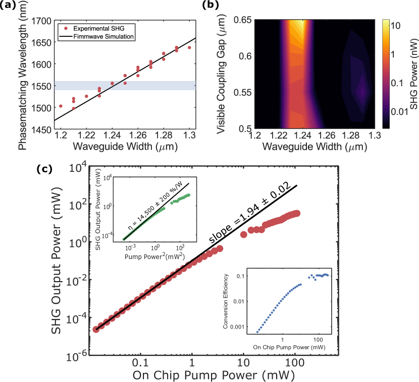
At low pump levels, SHG output power is known to increase quadratically with the pump power and deviates from this behavior with high pump power due to pump depletion. Fig. 2(c) depicts the pump power dependence of the SHG output power in a device with a 1.24 μm width and a 0.65 μm visible coupling gap. At low pump power, the variation of the SHG output power is close to the predicted quadratic dependence on the pump power, with a fitted slope of 1.94 0.02, whereas the SHG output power begins to deviate from the quadratic behavior at high pump power. The lower inset to Fig. 2(c) shows the absolute conversion efficiency (), which deviates greater than 50% from the predicted behavior when the on-chip pump power is greater than 3.5 mW and saturates to 11% when is greater than 35 mW. This deviation from the quadratic power dependence is observed in the high power regime, which indicates significant pump depletion and ultimately limits the maximum SHG efficiency (Fürst et al., 2010; Guo et al., 2016a). Looking to Eq. 1, we notice that varies linearly with with a slope equal to the SHG efficiency ; the upper inset to Fig. 2(c) shows this relation and a SHG efficiency of %/W for this device is found via a linear fit of the low power regime. We then use the experimentally measured values of and at infrared and near-visible regimes to derive a nonlinear coupling strength MHz. This nonlinear coupling strength, mode overlap factors calculated by FEM simulations, and relevant device parameters (Guo et al., 2016a) are used to derive a value of pm/V for the single-crystalline AlN device platform. This value is quite close to the 8.6 pm/V recently measured in thin films of MOCVD AlN at 1064 nm (Majkić et al., 2017) and is nearly three times higher than previously reported values for polycrystalline AlN (Gräupner et al., 1992; Xiong et al., 2012).
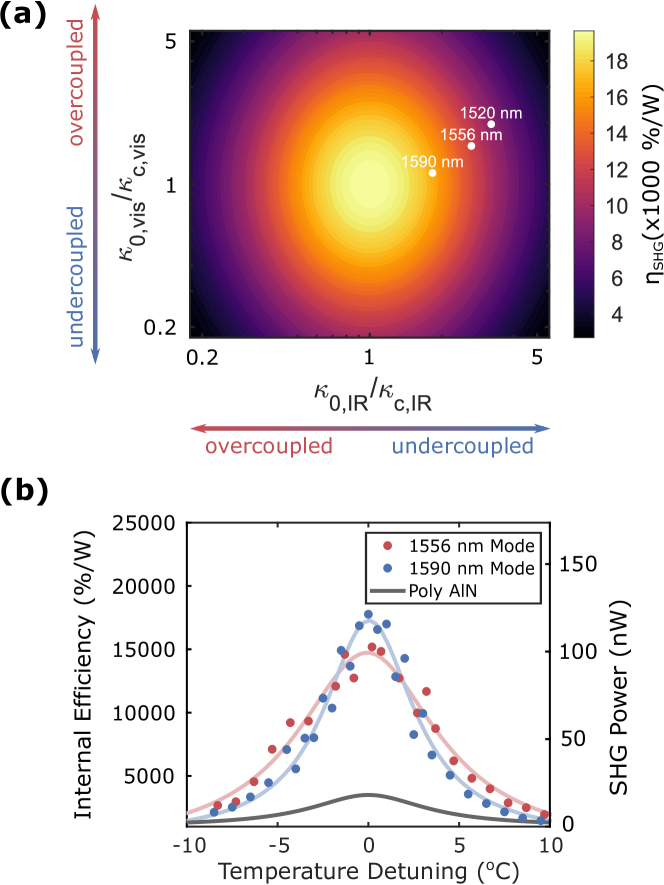
Finally, we look to Eq. 2 to optimize the SHG efficiency. As noted earlier, the SHG efficiency is optimized when the fundamental and second-harmonic resonances are both critically coupled. However, this proves difficult in practice as one (or both) resonances may deviate from critical coupling when varying the device geometries. Fig. 3(a) shows the effect of cavity coupling on the SHG efficiency (Eq. 2) using the derived MHz obtained above and experimentally measured intrinsic loss rates of MHz and MHz for infrared and near-visible modes, respectively. The SHG efficiency is maximized when both modes are critically coupled () and decreases as the modes become over- or under-coupled.
The device used in the previous pump-power experiment in Fig. 2 was nearly critically coupled for the near-visible resonance, but under-coupled for the IR resonance (), yet can still achieve a relatively high conversion efficiency of %/W. We notice that extinction ratio of the IR resonance increases when scanning from short to long wavelengths (Fig. 1(b)); the cavity coupling rate can be increased and a more ideal value for the SHG efficiency can be obtained by choosing a pump mode at a longer wavelength. Experimental values of are obtained at various wavelengths and are superimposed on the contour plot in Fig. 3(a), which indeed suggest that using a mode at 1590 nm may increase the experimental SHG efficiency. We systematically optimize the SHG output of optical modes at 1590 nm and 1556 nm by varying the global temperature of the chip to align the wavelengths of infrared and visible resonances, as shown in Fig. 3(b). With an input pump power (measured in the input fiber) of 260 μW, a maximum SHG output power of 120 nW and 110 nW are collected for 1590 nm and 1556 nm modes, respectively. After considering the transmission of 22 % and 10 % for IR and visible wavelengths, respectively, an on-chip (internal) SHG efficiency of 17,000 %/W and 15,000 %/W can be calculated for each mode. The observed SHG efficiencies are in good agreement with the theoretical values calculated in Fig. 3(a) for both modes as well as that calculated in Fig. 2(c) for the 1556 nm mode without fine thermal tuning. We calculate a 3000 %/W uncertainty in the calculated conversion efficiency, arising mainly from the 10 % relative error in measuring the absolute transmission for both infrared and visible wavelengths as well as amplitude noise from the high-sensitivity visible photodetector. This internal conversion efficiency is a seven-fold improvement compared to previous polycrystalline AlN devices (Guo et al., 2016a), manifesting our result as a new record for SHG among current integrated platforms. We attribute this record high SHG efficiency to the greatly increased optical factors at both infrared and near-visible wavelengths compared to previous device platforms as well as a relatively high material value obtained in this work. We do not believe a defect-related SHG proces plays a role at this time, as the effective value for surface charge SHG is typically one to two orders of magnitude less than that observed in AlN (Levy et al., 2011; Puckett et al., 2016).
In conclusion, we demonstrate a fabrication process to realize high quality AlN-on-sapphire nanophotonic devices for integrated nonlinear photonic applications. In the low pump power regime, an on-chip SHG conversion efficiency of 17,000 %/W (0.17 mW-1) is recorded, which is the new state-of-the-art thus observed among integrated platforms. At high pump power, pump depletion is observed at a relatively low pump power of 3.5 mW. The demonstrated high SHG efficiency paves the way for applications including low loss coherent frequency conversion (Guo et al., 2016c), on-chip comb self-referencing, as well as more efficient correlated photon-pair sources (Guo et al., 2016b).
This work is supported by DARPA SCOUT (W31P4Q-15-1-0006) and ACES programs as part of the Draper-NIST collaboration (HR0011-16-C-0118). H.X.T. acknowledges support funding from an AFOSR MURI grants (FA9550-15-1-0029), LPS/ARO grant (W911NF-18-1-0020), NSF EFRI grant (EFMA-1640959) and David and Lucile Packard Foundation.
References
- Cazzanelli et al. (2011) M. Cazzanelli, F. Bianco, E. Borga, G. Pucker, M. Ghulinyan, E. Degoli, E. Luppi, V. Véniard, S. Ossicini, D. Modotto, S. Wabnitz, R. Pierobon, and L. Pavesi, Nat. Mater. 11, 148 (2011).
- Chang et al. (2016) L. Chang, Y. Li, N. Volet, L. Wang, J. Peters, and J. E. Bowers, Optica 3, 531 (2016).
- Fürst et al. (2010) J. U. Fürst, D. V. Strekalov, D. Elser, M. Lassen, U. L. Andersen, C. Marquardt, and G. Leuchs, Phys. Rev. Lett. 104, 153901 (2010).
- Gromovyi et al. (2017) M. Gromovyi, J. Brault, A. Courville, S. Rennesson, F. Semond, G. Feuillet, P. Baldi, P. Boucaud, J.-Y. Duboz, and M. P. De Micheli, Opt. Express 25, 23035 (2017).
- Guo et al. (2016a) X. Guo, C.-L. Zou, and H. X. Tang, Optica 3, 1126 (2016a).
- Lin et al. (2016a) Z. Lin, X. Liang, M. Lončar, S. G. Johnson, and A. W. Rodriguez, Optica 3, 233 (2016a).
- Wang et al. (2017) C. Wang, X. Xiong, N. Andrade, V. Venkataraman, X.-F. Ren, G.-C. Guo, and M. Lončar, Opt. Express 25, 6963 (2017).
- Wolf et al. (2017) R. Wolf, I. Breunig, H. Zappe, and K. Buse, Opt. Express 25, 29927 (2017).
- Xiong et al. (2011) C. Xiong, W. Pernice, K. K. Ryu, C. Schuck, K. Y. Fong, T. Palacios, and H. X. Tang, Opt. Express 19, 10462 (2011).
- Roland et al. (2016) I. Roland, M. Gromovyi, Y. Zeng, M. El Kurdi, S. Sauvage, C. Brimont, T. Guillet, B. Gayral, F. Semond, J. Y. Duboz, M. de Micheli, X. Checoury, and P. Boucaud, Sci. Rep. 6, 34191 (2016).
- Surya et al. (2018) J. B. Surya, X. Guo, C.-L. Zou, and H. X. Tang, Optica 5, 103 (2018).
- Levy et al. (2011) J. S. Levy, M. A. Foster, A. L. Gaeta, and M. Lipson, Opt. Express 19, 11415 (2011).
- Wang et al. (2016) L. Wang, L. Chang, N. Volet, M. H. P. Pfeiffer, M. Zervas, H. Guo, T. J. Kippenberg, and J. E. Bowers, Laser Photon. Rev. 10, 631 (2016).
- Luo et al. (2017) R. Luo, H. Jiang, S. Rogers, H. Liang, Y. He, and Q. Lin, Opt. Express 25, 24531 (2017).
- Clemmen et al. (2009) S. Clemmen, K. P. Huy, W. Bogaerts, R. G. Baets, P. Emplit, and S. Massar, Opt. Express 17, 16558 (2009).
- Guo et al. (2016b) X. Guo, C.-l. Zou, C. Schuck, H. Jung, R. Cheng, and H. X. Tang, Light Sci. Appl. 6, e16249 (2016b).
- Sharping et al. (2006) J. E. Sharping, K. F. Lee, M. A. Foster, A. C. Turner, B. S. Schmidt, M. Lipson, A. L. Gaeta, and P. Kumar, Opt. Express 14, 12388 (2006).
- Jin et al. (2014) H. Jin, F. Liu, P. Xu, J. Xia, M. Zhong, Y. Yuan, J. Zhou, Y. Gong, W. Wang, and S. Zhu, Phys. Rev. Lett. 113, 103601 (2014).
- Guo et al. (2017) X. Guo, C.-L. Zou, H. Jung, Z. Gong, A. Bruch, L. Jiang, and H. X. Tang, (2017), arXiv:1704.04264 .
- Lin et al. (2016b) J. Lin, Y. Xu, J. Ni, M. Wang, Z. Fang, L. Qiao, W. Fang, and Y. Cheng, Phys. Rev. Appl. 6, 014002 (2016b).
- Xue et al. (2017) X. Xue, F. Leo, Y. Xuan, J. A. Jaramillo-Villegas, P.-H. Wang, D. E. Leaird, M. Erkintalo, M. Qi, and A. M. Weiner, Light Sci. Appl. 6, e16253 (2017).
- Kowligy et al. (2018) A. S. Kowligy, A. Lind, D. D. Hickstein, D. R. Carlson, H. Timmers, N. Nader, F. C. Cruz, G. Ycas, S. B. Papp, and S. A. Diddams, Opt. Lett. 43, 1678 (2018).
- Hickstein et al. (2017) D. D. Hickstein, H. Jung, D. R. Carlson, A. Lind, I. Coddington, K. Srinivasan, G. G. Ycas, D. C. Cole, A. Kowligy, C. Fredrick, S. Droste, E. S. Lamb, N. R. Newbury, H. X. Tang, S. A. Diddams, and S. B. Papp, Phys. Rev. Appl. 8, 014025 (2017).
- Guo et al. (2018) X. Guo, C.-L. Zou, L. Jiang, and H. X. Tang, (2018), arXiv:1804.06921 .
- Wang et al. (2014) C. Wang, M. J. Burek, Z. Lin, H. A. Atikian, V. Venkataraman, I.-C. Huang, P. Stark, and M. Lončar, Opt. Express 22, 30924 (2014).
- Ning et al. (2012a) T. Ning, H. Pietarinen, O. Hyvärinen, R. Kumar, T. Kaplas, M. Kauranen, and G. Genty, Opt. Lett. 37, 4269 (2012a).
- Ning et al. (2012b) T. Ning, H. Pietarinen, O. Hyvärinen, J. Simonen, G. Genty, and M. Kauranen, Appl. Phys. Lett. 100, 161902 (2012b).
- Pernice et al. (2012) W. H. P. Pernice, C. Xiong, C. Schuck, and H. X. Tang, Appl. Phys. Lett. 100, 223501 (2012).
- Liu et al. (2017a) X. Liu, C. Sun, B. Xiong, L. Wang, J. Wang, Y. Han, Z. Hao, H. Li, Y. Luo, J. Yan, T. Wei, Y. Zhang, and J. Wang, Opt. Express 25, 587 (2017a).
- Liu et al. (2017b) X. Liu, C. Sun, B. Xiong, L. Wang, J. Wang, Y. Han, Z. Hao, H. Li, Y. Luo, J. Yan, T. Wei, Y. Zhang, and J. Wang, Optica 4, 893 (2017b).
- Liu et al. (2018) X. Liu, C. Sun, B. Xiong, L. Wang, J. Wang, Y. Han, Z. Hao, H. Li, Y. Luo, J. Yan, T. Wei, Y. Zhang, and J. Wang, ACS Photonics 5, 1943 (2018).
- Liu et al. (2016) X. Liu, C. Sun, B. Xiong, J. Wang, L. Wang, Y. Han, Z. Hao, H. Li, Y. Luo, J. Yan, T. bo Wei, Y. Zhang, and J. Wang, Opt. Lett. 41, 3599 (2016).
- Lu et al. (2018) T.-J. Lu, M. Fanto, H. Choi, P. Thomas, J. Steidle, S. Mouradian, W. Kong, D. Zhu, H. Moon, K. Berggren, J. Kim, M. Soltani, S. Preble, and D. Englund, Opt. Express 26, 11147 (2018).
- Liu et al. (2017c) X. Liu, C. Sun, B. Xiong, L. Wang, J. Wang, Y. Han, Z. Hao, H. Li, Y. Luo, J. YAN, T. Wei, Y. Zhang, and J. Wang, in Conf. Lasers Electro-Optics (OSA, Washington, D.C., 2017) p. FTu3D.1.
- Fanto et al. (2016) M. L. Fanto, J. A. Steidle, t.-j. J. Lu, S. F. Preble, D. R. Englund, c. C. Tison, a. matthew Smith, g. A. Howland, kathy-anne Soderberg, P. Alsing, G. A. Howland, K. Soderberg, and P. M. Alsing, in Front. Opt. 2016 (OSA, Washington, D.C., 2016) p. FTh5G.6.
- Troha et al. (2016) T. Troha, M. Rigler, D. Alden, I. Bryan, W. Guo, R. Kirste, S. Mita, M. D. Gerhold, R. Collazo, Z. Sitar, and M. Zgonik, Opt. Mater. Express 6, 2014 (2016).
- (37) M. Rooks, “Conducting layer for HSQ resist,” .
- Guo et al. (2016c) X. Guo, C.-L. Zou, H. Jung, and H. X. Tang, Phys. Rev. Lett. 117, 123902 (2016c).
- Majkić et al. (2017) A. Majkić, A. Franke, R. Kirste, R. Schlesser, R. Collazo, Z. Sitar, and M. Zgonik, Phys. Status Solidi Basic Res. 254 (2017), 10.1002/pssb.201700077.
- Gräupner et al. (1992) P. Gräupner, J. C. Pommier, A. Cachard, and J. L. Coutaz, J. Appl. Phys. 71, 4136 (1992).
- Xiong et al. (2012) C. Xiong, W. H. P. Pernice, and H. X. Tang, Nano Lett. 12, 3562 (2012).
- Puckett et al. (2016) M. W. Puckett, R. Sharma, H.-H. Lin, M.-h. Yang, F. Vallini, and Y. Fainman, Opt. Express 24, 16923 (2016).