Spin-split conductance and subgap peak in ferromagnet/superconductor spin valve heterostructures
Abstract
We consider the separate spin channel contributions to the charge conductance in superconducting/ferromagnetic spin valve structures. We find that the up- and down-spin conductance contributions may have a very different behavior in the subgap bias region (i.e. there is a spin-split conductance). This leads to a subgap peak in the total conductance. This peak behavior, which can be prominent also in systems, is strongly dependent, in a periodic way, on the thickness of the intermediate ferromagnetic layer. We study this phenomenon using a numerical self consistent method, with additional insights gained from an approximate analytic calculation for an infinite structure. We study also the angular dependence on the relative magnetization angle between and of both the spin-split and the total conductance. We do so for realistic material parameters and layer thicknesses relevant to experimental studies on these devices. We also find that the spin-split conductance is highly dependent on the interfacial scattering in these devices, and we carefully include these effects for realistic systems. A strong valve-effect is found for the angularly dependent subgap peak conductance that is largely independent on the scattering and may prove useful in actual realizations of a superconducting spin valve device.
I Introduction
Interest in the use of superconductors in spintronic devices, such as spin valvestsyzu , has been growing despite an incomplete understanding of the underlying basic physics of such devices. One of the main goals in incorporating superconductors in new spintronic devices is to reduce their energy consumptionBhatti2017 . Superconducting spintronics also garners intrinsic scientific interest because of the intricate proximity effectsBuzdin2005 involved between ferromagnets () and superconductors (). Thus, superconducting spintronic devices, including spin valves , have been proposed and studiedigor ; esch ; zkhv ; wvhg ; kami ; birge ; transistor . The layers compose the spin valve portion, and is a normal metal spacer, which is needed to enable control of the relative magnetization orientation of the two ferromagnets. One of the ways in which superconducting spin valves differ from ordinary ones is that their transport properties are non-monotonic with the relative orientation of the ferromagnetic exchange fieldswvhg ; Moen2017 ; Moen2018 .
The scientific interest in the unusual and useful properties of structures arises from their antagonistic proximity effects. In ferromagnets, the exchange field works to split apart singlet Cooper pairs, favoring same-spin triplet states (). This leads to an proximity effect that differs drastically from that at interfaces. These proximity effects are very short ranged, and are oscillatory in positionBuzdin1990 ; Halterman2002 due to the Cooper pairs acquiring a center of mass momentumdemler . This spatial dependence is important when analyzing the layer thickness dependence of thermodynamic properties of layered structuresBuzdin2005 , including in ferromagnetic Josephson junctionsryaz2001 ; birge2018 , and transport properties in superconducting spin valve devicesBernardo2015 ; Moen2017 . Under certain conditions, it is possible for these structures to feature long range proximity effects. For a non-uniform magnetization texture such as in HolmiumBernardo2015 ; hoprl , or for heterostructures with two or more non-collinear ferromagnetic exchange fieldsberg86 ; hbv ; bvh ; zdravkov2013 such as the case we study, the spin singlet of the s-wave superconducting Cooper pair correlations can effectively be rotated into the triplet states with . A non-collinear exchange field is necessary, because otherwise commutes with the Hamiltonian and only the triplet state can be induced. Due to the symmetry of the s-wave Cooper pairs these triplet correlations in the ferromagnet are odd in timebvh or, equivalently, in frequencyberezinskii . These correlations are long ranged since they are not broken apart by the exchange fieldbvermp ; kalcheim ; singh ; ha2016 ; wvhg . This yields a unique spin-valve effect in structures where the triplet correlations, induced by a non-collinear magnetization angle between the ferromagnets, can lead to a non-monotonic angular dependence on the transport featureswvhg ; Moen2017 , as well as on the static physical properties such as the transition temperaturealejandro . This angular dependence motivates much of our study into superconducting spin-valve structures. By considering the spin-dependent charge transport in structures, we can gain further insight into this angular dependence of the superconducting spin valve. We are also interested in how this affects the spin dependence of the conductance in this structure, and compare it to the angularly independent system.
A charge current carries electrons and holes in both the spin-up and spin-down states, which add up to produce the total conductance of the circuit. When a device is spin polarized, we can see unusual changes to the conductance features arising from the difference in the spin channel transport, leading to each spin band having its own associated conductance that differs from that of the opposite spin channeljohnson1998 ; johnson2001 . The separate spin channel conductances can have features which diverge from those of the total conductance, which is why we collectively refer to the spin-polarized components of the conductance as the spin-split conductance. In a superconducting/ferromagnetic heterostructure, the interplay between each spin channel in the ferromagnet with the energy gap of the superconductor can lead to dramatic effects in the overall conductance. At low bias, this interplay is mediated by Andreev reflectionsAndreev in which an incoming electron is reflected as a hole and forms a Cooper pair in the superconductor. There are two types of Andreev reflection: ordinary Andreev reflection in which the electron/hole has opposite spin upon reflection, and anomalous Andreev reflection in which they have the same spin. It has been shownwvhg ; linder2009 ; visani ; niu ; ji that for interfaces, triplet proximity effects are correlated with anomalous Andreev reflection. Therefore, it is pertinent to consider these reflections when determining the spin-split conductance for and or systems.
In previous workMoen2017 , we have noted that the conductance versus bias voltage curves in structures can exhibit a “subgap” peak structure below the critical bias. We explain in this paper that in general the low bias structure of in these devices is due to spin split conductance behavior, and we study in some detail the features involved and what parameters influence them. Specifically, we calculate the spin-split conductance of and heterostructures and verify that the spin dependence of the conductance can lead to exotic behavior and unusual properties, e.g. in the layer thickness dependence in such structuresMoen2017 . By studying the spin-split conductance, we can gain a deeper understanding of the full conductance features studied thus far. We begin, in this work, with a simple analytic model of an structure with infinitely thick and layers and examine the thickness dependence of the ferromagnet for the spin-split conductance in an approximate non-self consistent approach. We then compare this model to a fully self-consistent numerical calculation for a finite nanoscale system. We then include a second ferromagnet to determine how the spin-split conductance can lead to the angular dependence in the total conductance. The numerical calculations are done by finding the self-consistent solution of the Bogoliubov de Gennes (BdG) equationsdegennes , which determine the pair potential of the superconductor, with the proximity effects fully being taken into account. We then use a transfer matrix procedure within the Blonder-Tinkham-Klapwijk (BTK) methodbtk to extract the conductance. We use realistic interfacial scattering strengths, as pertinent to good but imperfect experimental samples. We find that moderate interfacial scattering actually enhance the spin-valve effects in some cases, as we discuss in our analysis and conclusions below. We also use layer thickness values relevantalejandro to experimental studies of these devices. The exchange field of the ferromagnet and the coherence length of the superconductor are taken to ranges that correspond to the actual materials (such as Co and Nb) used so that our work can be more easily compared with experimental results. We perform our calculations in the low limit in order to best identify the spin-split conductance features that can be seen.
After having established the properties of spin-split conductance via these analytical and numerical methods, we then calculate the angular dependence of the conductance in the superconducting spin valve and establish how it is deeply related to the spin-split conductance. We also discuss how the interfacial scattering, which is an inevitable consequence of imperfect interfaces in fabricable devices, affect the spin-split features and the subgap peak conductance in these systems. From this study, we see a dramatic shift in the conductance for biases below the critical bas (CB) value, determined by the pair potential of the superconductor. This shift is oscillatory with the thickness of the layer, and it results in a conductance peak that occurs between the critical bias and zero bias. We find that this subgap peak in conductance can have a large angular dependence, producing a significant valve-effect. Thus, we hope that our work will lead to a better understanding of these devices for future application and motivate additional theoretical and experimental work.
II Methods
II.1 The basic equations
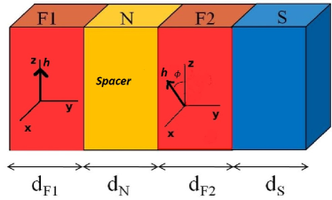
Since the methods we use here are those of Refs. [wvhg, ; Moen2017, ; Moen2018, ] we will merely, in this subsection, go over the main points to establish notation and to highlight certain theoretical features that we wish to study. Our focus is on the spin valve heterostructure, and we will carry on the development in this context. The geometry of the valve structure is represented qualitatively in Fig. 1. The layers are assumed to be infinite in the transverse direction and the -axis is taken normal to the layers.
The Hamiltonian of our system in terms of the usual creation and annihilation operators is,
| (1) | |||||
where is the Stoner field. We choose the axis to be along the internal field in the outer magnet (see Fig. 1), while forming an angle with the axis (and lying in the plane) inside the inner magnet . It vanishes in the superconductor and in the normal spacer . is the single particle Hamiltonian, in which we include the interfacial scattering.
Via a generalized Bogoliubov transformation, performed using the phase conventions of Ref. [wvhg, ] one can, in our quasi one dimensional geometry, rewrite the eigenvalue equation corresponding to the above Hamiltonian as:
| (2) |
where and are the position (i.e. ) and spin dependent quasiparticle and quasihole amplitudes in the Bogoliubov transformation. We use natural units: . The quasi one dimensional Hamiltonian is where is the transverse energy. Thus, Eq. (2) is a set of decoupled equations, one for each . is the layer dependent band width: we take here . is the interfacial scattering, which we assume to be spin-independent and parametrize as with being numbered from the left-most to the right-most interfaces (see Fig. 1). We define dimensionless barrier height parameters, , where is the Fermi speed in , which characterize the strength of the delta functions.
The calculation of the pair potential mustwvhg ; bagwell ; sols2 ; sols ; Moen2017 in principle be performed self consistently, in order to ensure that charge conservationbaym is preserved. The self consistency condition is:
| (3) |
with the summation being over all eigenstates and the prime indicating that it is limited to states with eigenenergies within a cutoff from the Fermi level. The quantity is the superconducting coupling constant, assumed to be in the singlet channel, and to be nonvanishing in only. To get a self-consistent result, we start with a suitable initial choice of and iterate Eqs. (2) and (3) until the input and output values of coincide. One can then derive the thermodynamic quantities from the self-consistent wavefunctionszkhv ; bvh , the results of which have been found to be in agreement with experimental workalejandro .
As mentioned in the Introduction we have considered also a simpler structure which can be solved analytically if one makes the additional approximation of treating the pair potential non-self-consistently, with a constant value of in . This system can be visualized by removing the left-most layer in Fig. 1. The analytic calculation is an approximation, done only as a means of comparison and of obtaining, as we shall see, some physical insights. A correct calculation requires a self-consistent approach. Also, we consider only one barrier at the interface of dimensionless strength .
II.2 Transport
We use the BTK formalismbtk to evaluate the conductance. We first calculate the reflection and transmission amplitudes for incoming electrons traveling perpendicular to the plane of our heterostructure and then use the BTK method to extract the conductance, in Sec. II.4, which is given in terms of the spin dependent Andreev and ordinary reflection amplitudes and . The incoming waves in terms of these amplitudes are compactly written in the form
| (4) |
for an incoming up spin particle in , while for the down spin case one has:
| (5) |
where the second spin index in the amplitudes and denotes the spin of the incoming particle, and the first that of the reflected wave. The wavevectors are:
| (6) |
with for up (down) spins. is the length of the wavevector corresponding to energy . Here and below all wavevectors are in units of and all energies in terms of .
II.3 Approximate analytic methods
If one foregoes treating the pair potential self-consistently, it is possible to derive expressions for the relevant amplitudes which are in principle analytic, although rather intricate. We do this here for an infinite heterostructure, where and are assumed to be of infinite thickness, but is finite. The expressions for the incident waves, now impinging from , are of the form given in Eqs. (4) and (5) but with a simplified wavevector structure involving only the spin independent wavevectors
| (7) |
For the intermediate layers, the eigenfunctions contain both left- and right-moving plane waveswvhg . Thus the wavefunction for intermediate layer has eight unknown coefficients. The layer contains right-moving quasiparticles and left-moving quasiholes, with fourwvhg unknown coefficients. Our plane wave expressions for and are exactly the same as Eqs. (8) and (10) in Ref. [wvhg, ] (with in the former) and we do not repeat them here. It should be recalled that in the equations for the (non-self-consistent) pair potential is a constant, , in .
We apply the continuity condition at each interface , , where for the infinite system, we conveniently choose the interface to be at and the interface to be at . The conditions on their derivatives are and similarly for the second interface. We can use a transfer matrix method to write these as matrices multiplied by their respective vector of unknown coefficients for each layer , as was explained in Ref. [wvhg, ]. Then, and , where denote that the wavefunctions are evaluated on the left or right side of the layer respectively and denotes the spin of the incoming electron in the layer. By solving and eliminating the intermediate layer coefficients, we find the eight total coefficients of both the and layer:
| (8) |
Solving these eight equations simultaneously for both spin-up and spin-down incoming electrons, we find the two sets of four reflection amplitudes and , one set for each incoming spin state , which we use to calculate the conductance in Sec. II.4.
Thus, the calculation is formally analytic. Although the full form solution for each reflection amplitude can not be written in a compact manner, knowing the form of the plane wave description lets us approximately determine the spatial dependence of the amplitudes. This spatial dependence comes from a combination of plane waves in , which are of the form , in which the wavevectors in the layer are defined by Eq. (6). In the zero bias limit, , we can express the wavevector for the forward conductance () as in our units, where we have dropped the particle/hole notation as these quantities are the same at zero bias. Thus if we write one such combination of plane waves, e.g. to lowest order in , we expect then to see a spatial periodicity with a wavelength such as (in dimensionless units ) at zero bias. These are the same as the well known oscillations of the Cooper pair amplitudes within the ferromagnetdemler . Similarly, means we can also expect oscillations of wavelength or, in dimensionless units, simply . In subsection II.4, we will use the absolute value squared of these amplitudes to calculate the conductance. Therefore, we expect all real coefficients with a or periodicity in the amplitude to result in a conductance with periodicities proportional to and respectively.
II.4 Extraction of the spin split conductance
From the above results one can extract the conductance using the BTK methodbtk . The current is related to the applied bias via the expression:
| (9) |
where is the Fermi function. The bias dependent tunneling conductance is which we evaluate in the low- limit. The conductance can be calculated using the reflection amplitudes and described in the above subsections, for either the self-consistent or non-self-consistent results. Combining the conductance contribution from incoming spin-up and spin-down electrons one has:
| (10) | ||||
where is given in natural units of conductance , and denotes the spin of the incoming electron. In Eq. (10), denotes the wavevector of the respective particle/hole in the first layer. In the case described in Sec. II.3, for both spins, while in the case is given by Eq. (6). The factors are included to take into account the different density of incoming spin up and spin down states in the layer for the system. In the system, denoting equal density. The quantities are the spin-up and spin-down conductances, which we collectively refer to as the spin-split conductance, since each component may drastically differ and “split” in behavior from that of the total conductance . The energy dependence of arises from the applied bias voltage . It is customary and convenient to measure this bias in terms of the dimensionless quantity where is the value of the order parameter in bulk material. We will refer to the dimensionless bias dependent conductance simply as . We will refer to the spin-split conductance in a similar fashion. In the spin valve structure, and also depend on .
Generally, and will differ significantly, however they are related to each other by a rotation around the axis in spin space. Using the unitary transformationhbv and taking the expectation value, we can define our spin-up and spin-down conductances, , in a basis rotated from that of the axis, , as:
| (11a) | |||
| (11b) | |||
In the system the angle can be thought of as the angle between the field in and the axis, since this basis rotation is exactly the same as a rotation in . However, this is not the case in the system when there is an actual angular mismatch. We can thus compare the change in the spin split conductance due to the angular mismatch to that arising from pure rotation in basis.
III Results
In this section we present our results for the spin-split conductance defined by Eq. (10) as explained in the text below it. We start (Sec. III.1), by analyzing a simple, system, with infinitely thick and layers, in a non-self-consistent manner, as derived in Sec. II.3. In that case the calculations can be performed analytically, and the results, although quantitatively inaccurate, illuminate a qualitative discussion that applies to all systems. We then move to the self-consistent approach (Sec. III.2) first briefly for a finite size system, so that we can gauge the degree of reliability of the analytic calculations, and then, in subsection III.3, we consider the realistic superconducting spin valve system. For reasons that will become clear below, we are particularly interested in how the conductance depends on the intermediate ferromagnetic layer thickness and on the interfacial scattering barriers, particularly that at the interface.
In presenting our results we use dimensionless units: all lengths are in units of and are denoted by capital letters such as , , and . The bias voltage is in units of the bulk value of the pair potential, . As mentioned above, the conductance is in natural units . Values of the dimensionless barrier parameters (introduced above) greater than unity would begin to approach the tunneling limit, while zero represents a perfect interface. We also set any wavevector mismatch parameters to unity, subsuming their effects in the phenomenological values. This reduces the number of parameters governing the system. With a minor exception for illustrative purposes, we set the exchange field in all ferromagnets (which we assume to be of the same material in the valve case) to be in our dimensionless units, where is the half-metallic limit, and we set the coherence length in our length units. The values of and chosen have been found to be suitable to the quantitative analysis of static quantities done on similar systems using Cobalt and Niobiumalejandro .
We have found that the most crucial geometrical parameter for our purposes is the thickness of the intermediate layer and consequently we examine, in each subsection, the conductance dependence on this layer thickness , or , for the or the spin valve system respectively. We also examine the dependence on the barrier at the or interface, and also, in Sec. III.3, on the barrier strengths at all the interfaces. In Sec. III.3, we also examine the dependence of the spin-split and total conductances on the mismatch angle of the exchange fields, and .
III.1 N/F/S conductance: analytic results
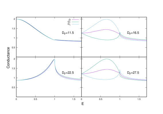
In this subsection we discuss the results of our analytic approach described in section II.3. To obtain analytic results, we have to abandon self consistency, so the results are only approximate. We consider an infinite system, with finite, varying thickness but infinite and . This is worthwhile, however, as from analytic results one can establish context and gain a degree of physical insight that is difficult to gather from our self-consistent numerical results discussed in the subsections below. The non-self-consistent results differ, of course, from the correct self-consistent ones. One obvious difference occurs near the critical bias (CB). For our analytic results the CB is always at since in the non-self-consistent case, for all in . In Figs. 2 and 3 we examine the spin-split conductance (i.e. the spin-up and spin-down components) and the total conductance, , defined by Eq. (10), as functions of applied bias. In Figs. 4 and 5 we plot the zero bias conductance (ZBC) and the critical bias conductance (CBC) respectively as functions of the thickness of the ferromagnetic layer .
The results plotted in Fig. 2 are for a moderately strong barrier, , which is a realistic value for a good interface, located at the boundary. The reason for studying this barrier is that even a small amount of interfacial scattering allows for the formation of a prominent feature that we wish to study: the subgap conductance peak. This is a peak in the conductance occurring for specific thicknesses of at biases between zero and the critical bias (the “subgap” bias region). As we shall see, the spin-split conductance components can vary dramatically especially near the CB. The total conductance is a combination of the components of the spin-split conductance. In this single layer system, the total is simply the average of the up and down spin-band contributions. When the spin-up and spin-down conductances are split from one another, we see a peak in the total conductance where the two differ the most. Examining the peak value of the conductance, we find a periodic behavior with , with a periodicity of in our dimensionless units. This can be traced, of course, to the well-known periodicitydemler of the Cooper pair amplitudes, reflected in the above given value, as has been discussed at the end of Sec. II.3.
The figure includes four panels, each for a different value of within one cycle of this periodic behavior. In the first and third panels, which correspond to a difference of about half a period, we see that the peak in the total conductance occurs at zero bias and at the critical bias respectively, while in the similarly separated second and fourth panels we see a subgap bias conductance peak. This subgap peak in the conductivity is similar to those reported in Ref. [Bernardo2015, ] for inhomogeneous structures, where in their tunneling conductance measurements. They find symmetrical, small peaks in the subgap region of the density of states, which they call the “double-peak spectra” and, for a subset of their samples, a single peak in the zero bias conductance, which they call the “zero peak spectra”. Here, we will refer to these peaks as the subgap bias and the ZBC peaks respectively. We believe these observed tunneling conductance peaks may be due to the spin-split conductance phenomenon we discuss below, with the “zero peak spectra” found for a small subset of their samples possibly being due to small fluctuations in the sample layer thicknesses, at fractions of a nanometer.
The total conductance peak moves away from zero bias in the first panel to a finite subgap bias value in the second. Increasing further, the peak moves to the critical bias in panel three, then returns in panel four to the same subgap bias value as in panel two. It goes back to zero bias, with a peak feature very similar to that in panel one for (not shown): at that point a whole period in has elapsed. In the first and third panels we see little difference between the subgap spin-up and spin-down conductances. On the other hand, we see a very large difference in the spin-split conductance for the second and fourth panels. In the second panel, the spin-down conductance has a large subgap peak, with reaching a value of before decreasing towards the CB, where there is a discontinuous change in slope (leading to what we describe as a “shoulder”). The spin-up conductance has the opposite behavior, with a dip in the subgap region that increases to a sharp cusp shaped peak at the CB. This spin-split conductance then yields a total with a local maximum at the spin-down conductance’s maximum, which is also the spin-up conductance’s minimum. In panel four, we see a very similar situation. However, the respective behaviors of the spin-up and spin-down conductances have reversed, with the spin-up conductance having an intermediate maximum and a shoulder critical bias feature, and the spin-down conductance having an intermediate minimum and cusp critical bias feature. In both of these panels, the CBC is also split between spin-up and spin-down, and the total conductance has a hybrid cusp-like behavior. There is then a crossing point, where each component (and the total conductance) meet, at a bias slightly below that of the CB.
In all four panels the ZBC is the same for the spin-up and spin-down conductances, and consequentially for the total . In ordinary Andreev reflection, a spin-up electron reflects into a spin-down hole, and vice versa. In the zero bias limit the electron and hole have equal energy. Thus, in the single layer case, the zero bias spin-up transmission amplitudes are the same as those for spin-down transmission, due to the symmetry of the electron/hole traveling in the spin-up/spin-down bands. We will see in Sec. III.3 that this is not the case when there is a second ferromagnetic layer.
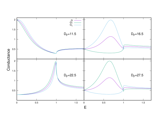
In Fig. 3 we repeat the plots in Fig. 2 but for a stronger barrier, . In all four panels we see in general a decrease in the conductance at all biases, with the remarkable and interesting exception of the peak value of the conductance, which remains high in all cases. In panel one, for example, we see no decrease in the ZBC, and similarly in panel three for the CBC. This leads to a “resonance” feature similar to that discussed in Fig. 6 of Ref. [Moen2017, ], where the ZBC is independent on the barrier strength. In panels two and four, we do see a moderate decrease in the average value of the total subgap conductance, but not in the maximum values of the spin-split conductance. Instead, there is a decrease in the minimum of the opposite spin component, as well as a general decrease in the ZBC and CBC. This leads to a much more pronounced subgap peak conductance than in the case. This feature is very resilient to high values of , it begins to deteriorate only well into the tunneling limit. A low value for makes the peak less obvious as the subgap conductance increases towards its maximum possible value of and the difference between the spin-up and spin-down conductances decreases.We have restricted our analysis of this simplified model to the case of only one barrier at the interface. Below, in Sec. III.3, we examine an system with barriers at each interface including .
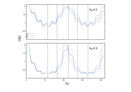
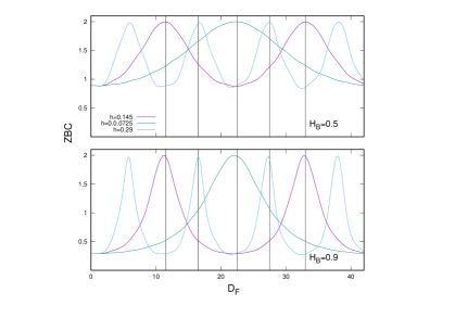
We now show specific details of the periodicity. In Fig. 4 we plot the zero bias conductance as a function of for (top panel) and (bottom panel), for (the only value we use in all of our figures except this one) and for and , half and double the original value. We do so to best demonstrate the dependence of the periodicity on . As mentioned above, the ZBC is equal for the spin-up, spin-down, and total conductances and therefore we only plot the total . The four leftmost vertical lines in each plot are the values of used in Figs. 2 and 3, and the fifth is for at which value one full cycle is complete for . We can clearly see here the dependence of the wavelength of the oscillation. For a value double the original, the wavelength is halved, and vice versa. The oscillatory behavior looks very regular and fairly sinusoidal at , except for some minor irregular variations which are more prominent for . However, for the larger barrier value of the bottom panel, the oscillatory pattern is less sinusoidal, with a sharper dependence of the ZBC on at the ZBC maxima and a broadening of the ZBC minima. For the stronger barrier only a reduced range of thicknesses have a ZBC peak conductance feature, which qualitatively agrees with what was foundBernardo2015 in non-homogenous structures. Near the vertical lines, we also see a slight change in the phase of the oscillation for the stronger barrier. The periodic behavior breaks down for values of of less than a quarter-period, where the ZBC becomes constant and independent on .
Following up on this we plot, in Fig. 5, the critical bias conductance as a function of , for both and (top and bottom panels respectively) at . We do so for the spin-split conductance components, which do not have the same CBC value, as well as for the total conductance. We see the same overall periodic structure as in the ZBC, with a phase difference, since the CBC maxima occurs at the ZBC minima. There is also a minor oscillatory behavior with wavelength superimposed on the broader oscillations: this is unobservable in the ZBC. The oscillations are explained in Sec. II.3. The spin-up and spin-down conductances cross over at the CBC maxima and they also converge at the CBC minima (where there are ZBC maxima). Between nodal points there is a difference in the spin-split conductance components that reverses between a dominant spin-up or dominant spin-down conductance. The separation becomes greater as increases, or as the barrier strength increases.
We have found, using approximate analytic results, a regular, periodic behavior in the conductance features as a function of the ferromagnetic layer thickness. We have also found a subgap bias conductance peak, the prominence of which increases with the strength of the scattering barrier at the interface. This peak is due to the splitting of the spin-up and spin-down conductances. This analysis will be helpful in interpreting the numerical results below.
III.2 N/F/S spin-split conductance
To make the discussion of our numerical spin valve results more understandable, we start with a brief discussion of a simpler finite size, structure, with a single barrier at the interface: this is similar to the case studied in our analytic results. The calculation is now numerical and fully self consistent.
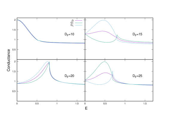
In Fig. 6 we plot the total conductance as a function of the rescaled bias voltage , together with the spin-up and spin-down conductance contributions. We do so in four panels corresponding to varying intermediate layer thickness , with fixed and in our dimensionless units. We take the scattering strength at the interface of . The variation in is chosen, as in our non-self-consistent results, to include a thickness range that demonstrates a full period of the conductance’s subgap peak behavior. The most obvious difference between the results of the non-self-consistent analytic calculation and those obtained via the numerical self-consistent procedure is that the latter case leads to a varying critical bias. This has been found and discussed previouslyMoen2017 and is directly related to the drop in the pair potential due to the proximity effect of the pair amplitude.
The first (upper left) panel of Fig. 6, corresponds to the situation where the ZBC is large and the CBC is low. The critical bias itself is significantly smaller in the self-consistent case, and there is little difference between the spin-up and spin-down conductance curves. Just as in the analytic case, this behavior is periodic with and occurs again near (not shown). In the second panel, we see the transition in the spin-split conductance, with a subgap peak in the total due to the opposing behavior of the spin-up and spin-down conductance components. The spin-up conductance displays a positive concavity and a cusp feature at the critical bias, while the spin-down conductance displays a negative concavity with a weaker shoulder feature at the CB, similar to those found in our analytic calculation. Although the critical bias conductance depends on the spin, the CB value itself does not. This is because both spin channels interact with the same effective pair potential, which for the single-ferromagnet system, and singlet pairing, is spin independent since the Hamiltonian commutes with .
In the third panel, we see the spin-split and total conductance peak locations converging towards the critical bias. Although not shown here, the relative behavior of the spin-up and spin-down conductance switches abruptly for slightly different values of , with a sharp transition similar to what is seen in the ZBC peaks of Fig. 5 in the analytic calculation. In the fourth panel, we see another subgap conductance peak similar to that in the second panel but now with the spin-split conductance components switching behavior, as was the case in our analytic calculation.
The spatial period we have considered corresponds to a wavelength for our value of . We conclude that the self-consistent behavior of the conductance qualitatively displays the same periodic behavior as revealed by the analytic non-self-consistent calculations. However, as mentioned above, the CB is now dependent on as can clearly be seen by looking across the four panels. In subsection III.3, we will find a further, more complex behavior by introducing an angular dependence on the system, which affects not only the spin-split conductance peaks but also the critical bias. As in the non-self-consistent, infinite case, the strength of the interfacial scattering at the interface enhances the peak conductance behavior, although we do not display this feature here. Furthermore, the increase in the barrier strength increases the critical bias value, making the analytic result approximation less inadequate in the strong-barrier case. Thus, the existence of the subgap conductance peak is verified for both the analytic and numerical calculation, and the peak is mostly independent of the barrier height .
III.3 F/N/F/S spin-split conductance
We now proceed, in this subsection, to the case of major theoretical and practical interest, where we include the outer ferromagnet, realistic, finite thicknesses and consider all interfacial barriers. We study, in the spin valve configuration, the dependence on the relative orientation of the exchange fields of the charge transport. This angular dependence is particularly important when applied to spin valves, as any angular dependence in the conductance constitutes a “valve effect” that can be exploited. We have studied such effects in previous workMoen2017 ; wvhg for a variety of physical parameters. In this subsection we continue to focus on the intermediate layer dependence and the oscillatory behavior of the peak conductance, which we have already noted in the case. Therefore, we concentrate on a small subset of interfacial scattering parameters, and on the spin-split effects that arise as varies.
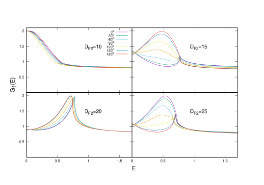
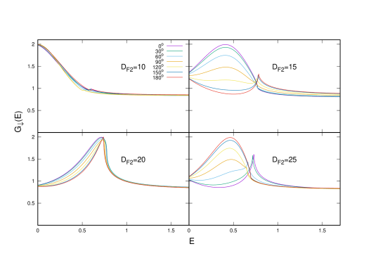
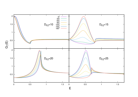
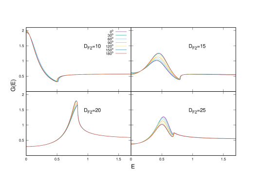
In Figs. 7 and 8 we plot the spin-split and the total conductance as a function of the misalignment angle for a single interfacial barrier, located at the interface, as was done in Fig. 6. Introducing this barrier best exhibits the behaviors of the peak conductance that can occur. We will later include one full set of barriers, in Fig. 9. We will also in this case be plotting the dependence of the conductances on the misalignment angle . Therefore, we subdivide each figure into three parts: (a) The spin-up conductance, (b) the spin-down conductance, and (c) the total conductance. In each of these parts the panels correspond to different values of , as indicated.
In Fig. 7 we plot the mentioned quantities as a function of the bias and for a moderate barrier value . Here, we see that the spin-up and spin-down components (Figs. 7(a) and 7(b) respectively) are highly dependent on the relative angle of magnetization. It is obviously no coincidence that the spin-up conductance very closely resembles that of the spin-down conductance for supplementary angles. Much of this resemblance is due to the change in being accounted for, in large part, by a purely mathematical rotation of the spin-split conductance as given by Eq. (11). Thus, it is seen that under a rotation by an angle , and vice versa. The angular dependence of each spin component closely resembles a combination of of the spin-up and spin-down conductance, rotated into the respective basis via Eq. (11) for . For the same reason, it should be no surprise that a subgap peak in the spin-split conductance is found near , since this can be largely described by a combination of the spin-up and spin-down conductances, as is the case with the total conductance. However, not all the differences in the features between the spin-up and spin-down conductances can be explained by this rotation, and a true angular dependence exists that is different for each component of the spin-split conductance. This yields a much more complex angular dependence in the total conductance (Fig. 7(c)).
In Fig. 7(a), we plot the spin-up conductance. We see a considerable spread in the critical bias. The angular dependence is relatively weak in the first panel and becomes much stronger in the other three. In the second panel, the CB increases for angles greater than and decreases for angles less than . In the third and fourth panels, we see the opposite: the CB decreases for and increases for . Recall that in the case we saw the spin-up and spin-down conductance swap behavior in panels two and four of Fig. 6, with a transition occurring in panels one and three. Similarly, we see here the CB behavior also making this transition in its angular dependence. The cusp and shoulder behavior of the CBC is not qualitatively changed by the introduction of the second ferromagnet. We also see a split in the ZBC.
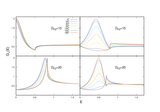
To complement the previous subplot, we next display, in Fig. 7(b), the spin-down conductance. As mentioned above, the behavior of this quantity is similar to that of the spin-up conductance, but with an angular dependence shifted by . The angular dependence of the ZBC and the CBC have dramatically changed, with opposite behavior. The ZBC no longer has a crossing point in the low bias regime. In effect, the introduction of the second ferromagnet takes the crossing node of the ZBC seen in the case (see Fg. 6) and moves it to the right in the spin-up conductance and to the left in the spin-down conductance. The CBC for the spin-down conductance experiences broadening, in direct opposition of the spin-up conductance, as can be seen best in the right hand panels (panels two and four). The angular dependence of the CB also broadens in these two panels. In panel three, we see the CB values move closer together and reverse the order of their angular dependence. This is explained by the spin-up conductance and spin-down conductance being at different phases in their periodicity. In panel three, we see the critical bias (and the overall conductance) behavior transition in its angular dependence from that of panel two to that of panel four. From the CB features plotted, we see, due to the spin-valve effect, that the spin-down conductance is slightly advanced in its phase, while the spin-up conductance lags behind.
Finally, in the last panel set, Fig. 7(c), we analyze the overall impact of the second ferromagnetic layer by plotting the total conductance, which can then be compared to that in Fig. 6. The total , as given by Eq. (10), is not, unlike in the case, simply the average of the spin-up and spin-down conductances, because the outer electrode is populated with a majority of spin-up electrons: the total conductance is now weighted more heavily towards the spin-up value. Therefore we see an angular dependence in the total conductance that is more reminiscent of that of the spin-up conductance. This can be seen in the similar CB angular dependence as well as the ZBC and CBC dependences. The combination of spin-up and spin-down conductance leaves us with a smaller subgap peak in the total , for all angles. Generally, we see a significantly reduced angular dependence when compared to the spin-split conductance, except for the ZBC and the CBC. We also see that the cusp and shoulder CB features are less pronounced. There is a crossing point in panels two and four as we saw with the spin-up conductance, however this is not an exact “node” as the conductance does not cross over at precisely the same bias for all angles. In panel three, we actually see a monotonically increasing peak conductance, even though neither the spin-up nor spin-down conductance feature this monotonic behavior. In this transition, the phase difference of the spin-up and spin-down oscillations with respect to has a greater impact on the CBC behavior of the total than for thicknesses such as in panels two and four.
In Fig. 8 we study the impact of the barrier strength on the spin-split conductance by increasing the parameter barrier value used in Fig. 7 from to , the value used in Fig. 3. We have found in previous workMoen2017 that an increase in barrier strength can lead to a decrease in angular dependence, particularly for the critical bias. We have also found above, in the case, that increasing the barrier strength can enhance the subgap conductance peak behavior. Below we analyze the combined effect that this change makes on our results.
In Figs. 8(a) and 8(b) we plot the spin-up and spin-down conductances, respectively, for this larger barrier value. We see the supplementary angle relation in the behavior of the spin-split conductance. We also see an angular dependence arise in the CB and the ZBC, as we did in Figs. 7(a) and 7(b), but this angular dependence is much smaller: this reflects the overall suppression of the proximity effects by the higher barrier. Furthermore, the difference between the spin-up and spin-down conductances (besides the switching of conductance behavior to supplementary angles) is greatly diminished. We do see a small broadening in the angular dependence of the CB, as well as a better defined crossing point. This leads to a total conductance that has, in the zero bias and critical bias regions, little angular dependence, as we see in Fig. 8(c). However, the subgap conductance peak still maintains a strong angular dependence, rivaling that of the case. This is because much of the angular dependence here comes from the difference in spin-up and spin-down electron populations emanating from the layer, in which the large difference between spin-up and spin-down conductance counteracts the decrease in angular dependence of the other conductance features. We also note that for higher barriers this subgap peak is more pronounced. The reason is twofold: the increased difference between the spin-up and spin-down conductances creates a large peak in the total , as we saw in Fig. 3, and the decrease in the angular dependence of the CB provides less overlap, which prevents the hybridizing of the cusp and shoulder CB behaviors, and makes the drop-off sharper near the CB.
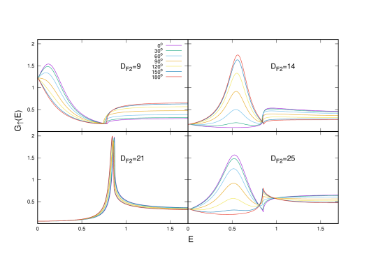
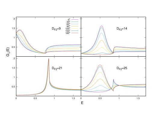
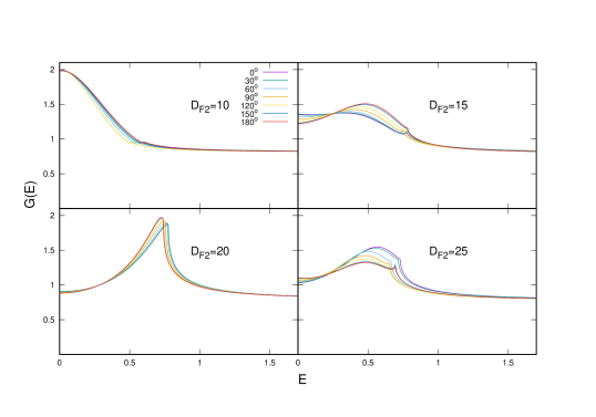
We now examine in Fig. 9 the realistic case where there are barriers at all three interfaces: , for the , , and interfaces respectively. These values are likely a good approximation to real experimental conditions as there are unavoidable interfacial defects even in the best prepared samples of heterostructures. The introduction of the barrier can slightly flatten the subgap peak conductance feature because a barrier at that interface reduces the proximity effect. However, this effect remains small, and when coupled with the moderate barriers, it leaves the conductance with well defined peaks, as we will see below. Having two interfacial barriers, particularly with similar values, can produce resonance effectsMoen2017 in the low bias conductance for certain thicknesses. There are a large number of parameter choices that can affect the conductance features in a variety of ways, but what is of interest here is how robust the oscillatory subgap peak behavior is.
In Fig. 9(a) we plot the spin-up conductance for these barrier values, and in Fig. 9(b) the spin-down conductance. The first thing to observe is the slight change in the values displayed in the first three panels from thhe values used in previous figures. We show, in the first panel, thickness values closest to the transition where the subgap conductance peak is now closest to zero bias. The ZBC peak conductance in panel one is very sensitive to small changes in , and it is important to try to tune precisely to that value. This sensitivity indicates that these barriers can have a large impact on the phase of the oscillatory behavior of the peak conductance. We see in our plot a large angular dependence at the peak bias, which is slightly greater than zero, but very little angular dependence on the ZBC. Also, the angular dependence in the subgap bias range is large, as we found in the single barrier, case (see Fig. 8). The high bias conductance () now displays a large angular dependence in panels one, two and four, but this dependence is much smaller in panel three where the subgap peak transitions at the CB. Examining the spin-up and spin-down conductances, we see greater broadening with in the CB and the CBC than we did in Fig. 8 in panels two and four. In panels one and two, we see some slight phase advancing/lagging, but the other conductance features are quite similar. These transitional panels have peaks which are sharper than in the previous results, and the ZBC peak is lower in value.
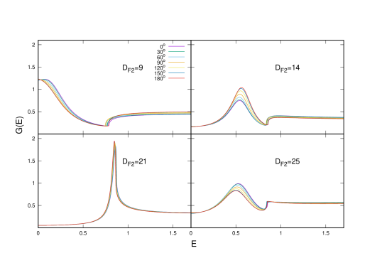
In Fig. 9(c) we plot the total conductance. Its behavior is similar to that of Fig. 8(c) but there are some key differences. Despite the barrier, the subgap conductance peak is sharper in panels two and four. Furthermore there is a larger, more noticeable angular dependence in the CB, as well as in the high-bias conductance. The ZBC, however, has a smaller angular dependence, but does still feature a small-bias crossing point before the subgap peak conductance. In panel three we see again an angular dependence in the CBC similar to that in Fig. 7(c). Overall, the salient point is that the subgap peak behavior is not only still present, but in fact more pronounced, with a large angular dependence in the peak conductance in panels two and four. This peak conductance is oscillatory with , with only a slight change in phase resulting from the introduction of realistic barriers. This robust angular dependence of the peak conductance can potentially be exploited, as the subgap conductance peak leads to an angularly dependent change in the excess currents at high biases.
IV Conclusions
We have analyzed here the spin-split conductance in spin valve systems using numerical, self-consistent methods. We have also considered systems using also an approximate but analytic method. We have found a peak in the subgap conductance that is periodic with the intermediate layer thickness. This peak conductance is due to the separate behavior of the contributions to the total conductance from incoming spin-up and spin-down electrons. We collectively call these contributions the spin-split conductance. Our results show that the subgap conductance peak position oscillates between the zero bias and the critical bias values as varies. We find that at least one spin band conductance has a maximum close to in our natural units at a single bias value in the subgap region, near where the opposite spin band has a minimum. At this subgap bias, we find a pronounced peak in the total conductance due to the spin-up and spin-down conductances being very different at this bias, while they converge in the ZBC and CBC. In systems with moderate or tunneling barriers, a peak in the conductance occurs at the critical bias before decreasing to normal conductancebtk . In the case we now see a second, subgap peak that is robust to interfacial scattering, with large angular dependence in the spin valve. The subgap peak and the ZBC resonance peak we find are qualitatively similar to the “double peak spectra” and the “zero peak spectra” seen in the tunneling conductance measurements, reported in Ref. [Bernardo2015, ], made via scanning tunneling spectroscopy in structures with a non-homogeneous (Holmium) ferromagnet. Our theoretical work, however, focuses on spin-valve structures.
Our spin valve results are numerical. It is usually difficult to gain physical intuition from purely numerical results. In an effort to gain additional intuitive understanding, we have used an approximate, non-self-consistent, analytic approach for an infinite structure. We examined the origin of the spatial periodic behavior by examining the ZBC and CBC as a function of the thickness of the layer. In both cases, we found that the periodic spatial dependence is due to the interaction of the spin dependent plane wave amplitudes in the ferromagnet, which leads to a wavelength of in the conductance peak ( is the exchange field of the intermediate ferromagnet). The location of the subgap conductance peak was found to oscillate between zero bias and the CB. The spin-split conductance as a function of bias consequently switches behavior between spin components with changes in layer thickness, transitioning across the CBC and ZBC peak conductances. In the analytic non-self-consistent approximation, there is no change to the critical bias itself, which is incorrect. We also established the effect of the interfacial barrier heights, on the conductance features. The subgap conductance peak is only weakly dependent on the barrier strength. Furthermore, when this peak occurs in the middle of the subgap region, the ZBC and CBC values decrease at a faster rate with increasing barrier strength, leaving a more pronounced subgap peak at higher barrier strengths.
Turning to the numerical self-consistent results for the spin valve, we find the same periodic effects, with an additional dependence of the spin-split conductance on the CB. This is also found for a finite structure. This dependence on the CB is reduced by high barriers. We analyze the dependence of the spin-split conductance on the angle between the internal exchange fields in the magnets and , in the system. Part of the angular dependence of the spin-split conductance in this system can be attributed to rotations in spin space (see Eq. (11)) but since (except at and ), does not commute with the Hamiltonian, we find that this dependence on is beyond that arising from a choice of spin quantization axis. This affects the CB, the CBC, and the ZBC in different ways for the spin-up and spin-down components, causing broadening of the CBC peaks and CB values, as well as shifting the crossing points where is approximately equal for all angles . From our analysis we conclude that the phase of the periodic dependence is angularly dependent for both components of the spin-split conductance: the thickness at which the behavior transitions depends on . There is a general shift in the spin-split conductance’s bias dependence, in opposite directions for each component, with a nodal point, located at zero bias in the system, shifting to higher bias values for spin-up and to lower ones for spin-down. The end result is that the total conductance has a complex angular dependence, where the subgap peak becomes less prominent, as the relative shift of the spin-split conductance means that each component’s respective (at supplementary angles) extrema are no longer aligned, leaving their combination (i.e. the total conductance) more smeared, and the other conductance features less pronounced. Nevertheless, a subgap conductance peak with a very strong angular dependence remains in the structure. This angular dependence is protected by the subgap peak, which does not diminish strongly with increasing barriers.
The subgap conductance peak, due to the spin-split conductance, is an important and prominent feature that can be exploited in future superconducting spintronic devices. One of our primary goals here has been to determine and improve the efficacy of a superconducting spin valve in which the valve effect is defined by the angular dependence of the exchange fields. The subgap peak is well defined when the interface between the superconductor and the valve is reasonably clean, even when the interfacial scattering within the valve is non-negligible. Although this can lead to very low angular dependence when the peak conductance is at zero bias or at the CB, the angular dependence is large and robust against interfacial scattering for definite values of the intermediate ferromagnetic layer thickness. By tuning the thickness to one of these intermediate values, a valve effect in the excess current can be attained, as we see then a very large angular dependence in the spin-split and total conductance. This would have a considerable effect on the quality of such spin valve devices.
Acknowledgements.
The authors thank I.N. Krivorotov (University of California, Irvine) for many illuminating discussions on the experimental issues. They are very grateful to Chien-Te Wu (National Chiao Tung University) for many helpful discussions on aspects of this problem. This work was supported in part by DOE grant No. DE-SC0014467References
- (1) E. Tsymbal and I. Žutić, Handbook on spin transport and magnetism, CRC Press, Boca Raton, Florida (2012).
- (2) Sabpreet Bhatti, Rachid Sbiaa, Atsufumi Hirohata, Hideo Ohno, Shunsuke Fukami, S.N. Piramanayagam, Spintronics based random access memory: a review, Materials Today, ISSN 1369-7021 (2017).
- (3) A. I. Buzdin, Rev. Mod. Phys. 77, 935 (2005).
- (4) I. Žutić, J. Fabian, and S. Das Sarma, Rev. Mod. Phys. 76, 323 (2004).
- (5) M. Eschrig, Rep. Prog. Phys. 78, 104501 (2015).
- (6) J. Zhu, I.N. Krivorotov, K. Halterman and O.T. Valls, Phys. Rev. Lett. 105, 207002 (2010).
- (7) C-T Wu, O.T. Valls and K. Halterman, Phys. Rev. B90, 054523, (2014).
- (8) T. Yu. Karminskaya, A.A. Golubov, and M. Yu. Kupryanov, Phys. Rev. B84, 064531 (2011).
- (9) Nevirkovets, I. P., Chernyashevskyy, O., Prokopenko, G. V., Mukhanov, O. A. and Ketterson, J. B. Superconducting-ferromagnetic transistor. IEEE Trans. Appl. Supercond. 24, 1800506 (2014).
- (10) E. C. Gingrich, B. M. Niedzielski, J. A. GLick, Y. Wang, D. L. Miller, R. Loloee, W. P. Pratt Jr, N. O. Birge, Nature Physics 12, 564-567 (2016).
- (11) E. Moen, O.T. Valls, Phys. Rev. B95, 054503 (2017).
- (12) E. Moen, O.T. Valls, Phys. Rev. B97, 174506 (2018).
- (13) Buzdin, A. I., and M. Y. Kuprianov, Pisima Zh. Eksp. Teor. Phys. 52, 1089-1091 [JETP Lett. 52, 487-491 (1990)].
- (14) K. Halterman and O. T. Valls, Phys. Rev. B66, 224516 (2002).
- (15) E. A. Demler, G. B. Arnold, and M. R. Beasley, Phys. Rev. B55, 15174 (1997).
- (16) V. V. Ryazanov, V. A. Oboznov, A. Yu. Rusanov, A. V. Veretennikov, A. A. Golubov, and J. Aarts Phys. Rev. Lett. 86, 2427 (2001).
- (17) Bethany M. Niedzielski, T. J. Bertus, Joseph A. Glick, R. Loloee, W. P. Pratt, Jr., and Norman O. Birge Phys. Rev. B 97, 024517 (2018).
- (18) A. Di Bernardo, S. Diesch, Y. Gu, J. Linder, G. Divitini, C. Ducati, E. Scheer, M.G. Blamire, and J.W.A. Robinson, Nat. Commun. 6, 8053 (2015).
- (19) C.T. Wu, O.T. Valls, and K. Halterman, Phys. Rev. Lett. 108, 117005 (2012).
- (20) F.S. Bergeret, A.F Volkov, and K.B. Efetov, Phys. Rev. Lett. 86, 3140 (2001); Phys. Rev. B68, 064513 (2003).
- (21) K. Halterman, P. Barsic and O.T. Valls, Phys. Rev. Lett. 99 127002 (2007).
- (22) P.H. Barsic, O.T. Valls and K. Halterman, Phys. Rev. B75, 104502 (2007).
- (23) V. I. Zdravkov, J. Kehrle, G. Obermeier, D. Lenk, H.-A. Krug von Nidda, C. Miller, M. Yu. Kupriyanov, A. S. Sidorenko, S. Horn, R. Tidecks, and L. R. Tagirov Phys. Rev. B87, 144507 (2013).
- (24) V. L. Berezinskii, JETP Lett. 20, 287 (1975).
- (25) F.S. Bergeret, A.F Volkov, and K.B. Efetov, Rev. Mod. Phys. 77, 1321 (2005).
- (26) Y. Kalcheim, O. Millo, A. Di Bernardo, A. Pal and J.W. Robinson, Phys. Rev. B92, 060501 (2015).
- (27) A. Singh, S. Voltan, K. Lahabi, and J. Aarts, Phys. Rev. X 5, 021019 (2015).
- (28) K.Halterman and M. Alidoust, Phys. Rev. B 94 064503 (2016).
- (29) A. A. Jara, C. Safranski, I. N. Krivorotov, C.-T. Wu. A. N. Malmi-Kakkada, O. T. Valls, and K. Halterman, Phys. Rev. B89, 184502 (2014).
- (30) M. Johnson, Phys. Rev. B58, 9635 (1998).
- (31) M. Johnson, Physica E 10, 472 (2001).
- (32) A. F. Andreev, Sov. Phys. JETP 19, 1228 (1964).
- (33) J. Linder, T. Yokoyama, and A. Sudbø, Phys. Rev. B79, 224504 (2009).
- (34) C. Visani, Z. Sefrioui, J. Tornos, C. Leon, J. Briatico, M. Bibes, A. Barthélémy, J. Santamaría, and Javier E. Villegas, Nature Phys. 8, 539 (2012).
- (35) Z. P. Niu, Europhys. Lett. 100, 17012 (2012).
- (36) Y.-Q. Ji, Z.-P. Niu, C.-D. Feng, and D.-Y. Xing, Chinese Phys. Lett. 25, 691 (2008)
- (37) P. G. de Gennes, Superconductivity of Metals and Alloys (Addison-Wesley, Reading, MA, 1989).
- (38) G. E. Blonder, M. Tinkham, and T. M. Klapwijk, Phys. Rev. B25, 4515 (1982).
- (39) P.F. Bagwell, Phys. Rev. B49, 6841 (1993).
- (40) F. Sols and J. Ferrer, Phys. Rev. B49, 15913 (1994).
- (41) J. Sanchez-Canizares and F. Sols, Phys. Rev. B55, 531 (1997).
- (42) G. Baym and L.P. Kadanoff, Phys. Rev. 124, 287 (1961).