Lithium-ion conducting glass ceramics for electrostatic gating
Abstract
We explore solid electrolytes for electrostatic gating using field-effect transistors (FETs) in which thin WSe2 crystals are exfoliated and transferred onto a lithium-ion conducting glass ceramic substrate. For negative gate voltages () the devices work equally well as ionic liquid gated FETs while offering specific advantages, whereas no transistor action is seen for . For the devices can nevertheless be driven into the ambipolar injection regime by applying a large source-drain bias, and strong electroluminescence is observed when direct band-gap WSe2 monolayers are used. Detecting and imaging the emitted light is much simpler in these FETs as compared to ionic liquid gated transistors, because the semiconductor surface is exposed (i.e., not covered by another material). Our results show that solid electrolytes are complementary to existing liquid gates, as they enable experiments not possible when the semiconductor is buried under the liquid itself.
Modulating the charge carrier density at the surface of semiconductors or insulators is commonly
done by means of electrostatic gating in field-effect transistors (FETs), employing conventional solid state dielectrics. In these devices, dielectric breakdown typically limits the maximum accumulated density to approximately 1013 cm-2. Drastically higher carrier density values –up to 1015 cm-2, corresponding roughly to one electron per surface atom– can be reached by employing ionic liquids or gels, Panzer, Newman, and Frisbie (2005); Shimotani et al. (2006, 2007); Ueno et al. (2008); Yuan et al. ; Scherwitzl et al. (2010); Ueno et al. (2011); Ye et al. (2011, 2012); Braga et al. (2012); Shi et al. (2015)
which exploit the very large capacitance (1-50 F/cm2)Yuan et al. associated to the thin (nanometer) interfacial double layer. As a result, ionic gated FETs could be used to demonstrate the occurrence of gate induced superconductivityUeno et al. (2008, 2011); Jo et al. (2015); Shi et al. (2015); Costanzo et al. (2016) at the surface of large gap semiconductors, to generate electroluminescence by enabling simultaneous injection of electrons and holes in different semiconducting materialsJo et al. (2014); Zhang et al. (2014); Ponomarev et al. (2015); Gutiérrez-Lezama et al. (2016) and to develop new forms of spectroscopy useful to characterize 2D semiconductors Braga et al. (2012); Lezama et al. (2014); Ponomarev et al. (2015); Xu et al. (2015); Gutiérrez-Lezama et al. (2016); Prakash and Appenzeller (2017).
Despite these impressive achievements, current ionic-gated FETs suffer from different drawbacks. An important issue is that in all devices realized so far the ionic liquid (or gel) covers the gated material, impeding the use of different experimental techniques that rely on surface sensitive probes (e.g., scanning tunneling microscopy and spectroscopy, photoemission spectroscopy, etc.). The covering liquid also adds considerable complexity to all experiments in which emission of light from the gated material is of interest, since it can absorb or deflect the light and alter the signalJo et al. (2014). Finally, besides practical problems such as the very strong sensitivity to air and humidityCapelli et al. (2010), ionic liquids also pose constraint on device fabrication and on the type of structures that can be realized, because it is virtually impossible to perform any additional nano-fabrication step after deposition of the liquid itself.
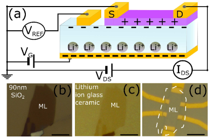
To address these problems we started exploring the possibility to substitute the liquid/gel electrolytes that have been employed until now with solid electrolytes. To this end, we have identified as promising candidates ion-conductive glass ceramics (ICGCs)Xu et al. (2007); Knauth (2009); Hayashi et al. (2012), in which Li+ or Na+ ions are free to move within a solid framework composed of different oxide materials. ICGCs are used as components in batteries (separators, electrolytes and cathodes), are known to have a high ionic conductivity (10-3 - 10-4 Scm-2)Xu et al. (2007); Knauth (2009); Hayashi et al. (2012), and to be stable under ambient conditions. The strategy that we follow to realize a FET device is to deposit a layer of semiconductor on top of a Li-ICGC substrate with a back metallic layer acting as a gate and micro-fabricated contacts enabling transport measurements (see scheme in Fig. 1a). In such a configuration, device operation is conceptually similar to that of conventional liquid electrolyte devices: upon application of a gate voltage, the Li+ or Na+ ions in the glass matrix move creating a space charge region near the surface due to depletion or accumulation of positively charged ions (depending on the gate voltage polarity), allowing the potential to be transferred from the gate electrode to the device.
Despite the conceptual similarity, it is essential to investigate the detailed aspects of the device response, as in practice they may differ significantly from the case of ionic-liquid gated FETs. For instance, it remains to be seen whether in solid electrolytes the spatial extension of the space charge regionParadisi, Biscaras, and Shukla (2015) at the surface is sufficiently small to generate the large required electrical capacitance. It is also unclear whether devices can function properly for both polarities of applied gate voltage. Indeed, while for a negative gate voltage the ions are attracted to the gate and no problem is expected, for a positive applied gate voltage ions are pushed toward the device. As Na+ –and even more Li+– ions are known to be very mobile, they may cause unwanted effects of none-electrostatic nature (e.g., intercalation, chemical reactions, etc.)Hermann et al. (1973); Woollam and Somoano (1976); Biscaras et al. (2015); Yu et al. (2015); Sterpetti et al. (2017), thereby preventing appropriate transistor operation.
To test the operation of Li-ICGC FETs we have realized devices based on thin exfoliated semiconducting transition metal dichalcogenides (TMDs), whose well-studied behavior in ionic liquid FETs provides an excellent referenceChuang et al. (2014); Pradhan et al. (2015); Wang et al. (2015); Prakash and Appenzeller (2017); Pudasaini et al. (2017) (most of the work discussed here is based on devices realized with WSe2 crystals purchased from 2D semiconductors). We find that upon the application of a negative gate voltage electrostatic doping works properly and allows reaching hole densities as high as 7 x 1013 cm-2, comparable to values achieved by ionic-liquid gating on several TMDsBraga et al. (2012); Lezama et al. (2014); Zhang et al. (2012) (the largest accumulated hole density in common semiconducting TMDs is typically smaller than the largest possible electron densityBraga et al. (2012)). For this gate voltage polarity, virtually all our devices exhibit high-quality transistor characteristics. Upon the application of positive gate voltage, however, no FET action is seen, confirming that effects other than simple electrostatics play a role when alkali ions are pushed to the surface. It is nevertheless possible to bias the devices into the ambipolar injection regime (i.e., with electrons and holes simultaneously injected at opposite contacts) by applying a negative gate bias concomitantly with a larger negative source-drain bias. In this regime, when a direct-gap monolayer WSe2 is used as transistor channel, electro-luminescence from exciton recombination is clearly observed. We find that controlling the induced electroluminescence is much easier than in ionic-liquid gated FETs, because the transistor channel is directly exposed to air and not buried under the ionic liquid/gel itself. Overall, our results demonstrate that Li+-ICGCs substrates can be implemented as gate dielectrics in actual devices with a number of advantages over conventional ionic-liquid/gel gated transistors.
The fabrication of WSe2 devices on Li-ICGC substrates consists of several steps. Thin WSe2 crystals are exfoliated onto Si/SiO2 substrates (see Fig 1b), and subsequently transferred onto commercially available 150 m thick ICGCs substrates purchased from MTI corporation (see Ref. (36) for the material data sheets and additional information), via a pick-up and release technique based on PC/PDMS stacksZomer et al. (2014). This proved necessary because even relatively thick (e.g., 10 nm) exfoliated crystals exhibit extremely small contrast on ICGCs substrates and are very difficult to identify unless dark field imaging is employed (see Fig. 1c and Fig. 1d, which compare dark and bright field optical microscope images of a same WSe2 monolayer). Electrical connections to the transferred crystals –as well as a reference electrode on top of the ICGC substrate– are then realized by means of fully conventional electron beam lithography, evaporation of Pt/Au films and lift-off. Fig. 1d shows an optical microscope image of a complete monolayer WSe2 device. Electrical measurements on more than ten devices realized with monolayer, bilayer and thicker crystals, all showing the same transistor behavior, were performed using a SR830 lock-in amplifier, Keithley 2400 source/measure unit, Agilent 34401A digital multimeters, and home-made voltage/current amplifiers. In some cases, measurements were performed with an Agilent Technology E5270B parameter analyzer, which gave identical results.
We start the characterization of Li-ICGC gated devices by measuring the FET transfer curve (source-drain current as a function of gate voltage ) for negative . Fig. 2a shows the current in the linear regime for different values of applied source-drain voltage (=1, 4, and 10 mV). The current scales linearly with , as shown by the fact that measurements at different lead to the same square conductance (see Fig. 2b; the identical conductivity found in successive measurements also illustrates the excellent reproducibility and stability of the devices). The threshold voltage for hole conduction is V, after which the current measured for mV rapidly reaches hundreds of nA, much larger than the leakage current typically measured (of the order of 1 nA or less, see Fig. 2c). The measured ON/OFF ratio (; see Fig. 2d) is determined by the current noise floor of our experimental set-up. From these measurements the maximum hole density accumulated at V is estimated by comparing the conductivity to the one measured on ionic-liquid gated WSe2Prakash and Appenzeller (2017) and other semiconducting TMD FETs Braga et al. (2012); Lezama et al. (2014); Zhang et al. (2012), at a same difference between threshold and applied gate voltage. The conductivity values in Li-ICGC and ionic-liquid gated devices are comparable, and using a characteristic hole mobility value of cm2/Vs Braga et al. (2012); Lezama et al. (2014); Zhang et al. (2012) we estimate the largest density of accumulated holes to be 7 x 1013 cm2/Vs. These results, obtained on a transistor realized on an exfoliated WSe2 crystal that is approximately 15 nm thick, are representative of what we commonly observed in many different Li-ICGC transistors that we investigated.
Other aspects of the data point to the quality of Li-ICGC FETs. One is the value of the sub-threshold swings , extracted from the logarithmic plot of -vs- (See Fig. 2d). We obtain mV/dec, fully comparable to the values found in ionic-liquid gated FETsBraga et al. (2012); Lezama et al. (2014); Xu et al. (2015), and very close to the ultimate room temperature limit of 60 mV/decade. Finding that approaches 60 mV/decade provides a direct confirmation of the large capacitanceM. Sze and Kwok (2006); Braga et al. (2012) of the glass ceramic gates. Another aspect is the virtually complete absence of hysteresis upon sweeping up to large negative voltages and back, which was observed in essentially all devices for sweeping rates up to mV/s upon repeatedly cycling the gate voltage. In contrast, in ionic-liquid gated FETs a somewhat larger hysteresis is often found when operating the devices under identical conditions. Finally, in nearly all Li-ICGC gated FETs investigated, the efficiency of the gate –defined as the ratio between the voltage measured at the reference electrode and the applied gate voltage – is reproducibly close to 100% (see Fig. 2e), indicating that the applied VG drops almost entirely across the ceramic/channel interface. This is consistently better than the 60-80% efficiency typically observed in ionic-liquid gated devices (see, for instance, reference 17).
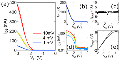
It follows from these considerations that –under a negative applied gate voltage– the performance of our Li-ICGC gated devices is fully comparable to that of ionic-liquid gated FETs, and even superior in a number of regards. The situation is however very different under the application of a positive gate voltage, in which case no transistor action was ever observed in our measurements. That something unusual happens in the Li-ICGC devices for is clearly apparent from the plot of -vs- in Fig. 2e, in which we see that does not increase upon increasing , but remains pinned at a small positive value. This behaviour clearly indicates that upon the application of a positive , the action of the gate is not determined by simple electrostatics: some other phenomenon likely related to the accumulation of a large density of Li ions at the surface (possibly the formation of a metallic Lithium layer sufficient to screen the applied gate voltage) prevents the devices to be operated in electron accumulation mode.
We now proceed to analyze the device output characteristics (-vs- measured at fixed, negative ). Fig. 3a shows data obtained from the same device whose transfer curves are shown in Fig. 2a. The expected transistor behaviour is apparent, with the current initially increasing linearly at small and exhibiting full saturation due to pinch-off when . Upon increasing well past the onset of saturation, a sharp increase of is seen in all devices investigated. This is shown in Fig. 3b, with data measured on a Li-ICGC device realized with a WSe2 monolayer. Such an increase occurs when is sufficiently large to invert the potential of the semiconducting channel at the drain contact. When that happens, charge carriers of opposite polarity are injected by the source and drain electrodes and the current is carried simultaneously by electrons and holes that recombine inside the channel. This is the so-called ambipolar injection regimeKang and Frisbie (2013) commonly observed in ionic-liquid gated FETs based on most semiconducting TMDsBraga et al. (2012); Zhang et al. (2012, 2013); Lezama et al. (2014); Chuang et al. (2014). In Li-ICGC gated transistors, detecting the occurrence of this regime is particularly interesting, because the absence of any current upon the application of a positive might have suggested that electron conduction may not happen. The data in Fig. 3b shows that this is not the case.
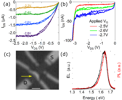
To obtain a compelling confirmation that electrons and holes are simultaneously carrying current we search for electroluminescence, which is expected in the ambipolar injection regime if the semiconductor has a direct band-gap. This is the case for monolayers WSe2 and we indeed find that –in the ambipolar injection regime– current flow is accompanied by light emission. To detect the emitted light we mounted our WSe2 monolayer device inside a vacuum chamber with optical access under an optical microscope, and used a common digital camera to take images (see Fig. 3c). Light is emitted rather uniformly across the entire device, at the position where electrons and holes meet. To identify the process responsible for light emission we measured the spectral dependence of the intensity using an Andor Shamrock spectrometer. We find that the electroluminescence spectrum coincides nearly perfectly with the spectral dependence of monolayer WSe2 photoluminescence, as shown in Fig. 3d, which allows us to conclude that electroluminescence is due to recombination of direct excitons (photoluminescence was measured using a Fianium Supercontinuum laser coupled to a monochromator at = 610 nm at a power of 10 W to excite the WSe2 monolayer). We remark that the use of the glass ceramic gate allows for a direct comparison of both spectra without having to subtract a background, as we found necessary to do in similar ionic-liquid gated devices based on WS2 monolayersJo et al. (2014). This shows that the optical signal originating from the device is stronger and cleaner as compared to the case of ionic-liquid gated devices, because on Li-ICGC FETs no other material is present on top.
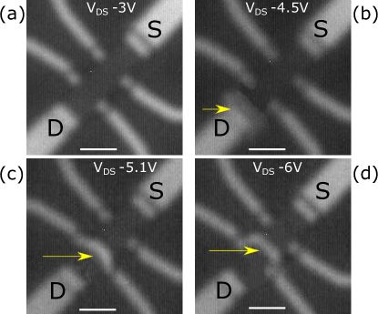
Finally, we discuss the evolution of the emitted light upon increasing . Fig 4a-d show microscope images of a monolayer WSe2 FET as is increased from -3 V to -6 V ( V in all cases). For V (Fig. 4a) the device is very close to the onset of the ambipolar injection regime (see Fig. 3b) and no light emission is detected yet. At V (Fig. 4b) light emission starts to be clearly visible close to the drain electrode. A further increase in ( V in Fig. 4c and V in Fig. 4d) causes light emission to be progressively shifted inside the transistor channel, away from the drain and towards the source contact. For all investigated bias values, light emission occurs from a line across the channel, approximately perpendicular to the current path. This behavior originates from the presence of a pn junction in the FET channel Zaumseil, Friend, and Sirringhaus (2006); Bisri et al. (2009); Kang and Frisbie (2013); Jo et al. (2014); Zhang et al. (2013), whose initial formation takes place near the contact where the local channel potential is reversed first due to the application of a large and negative source-drain bias. Increasing the bias leads to a shift of the position of the pn junction that follows from simple electrostatic considerations (see, e.g., Ref. (39)). Note that the observation of such an ideal evolution eliminates any possible scenarios responsible for light emission other than the formation of a pn junction inside the channel, such as the electrons being injected from the contact due to hot carrier effects caused by the high lateral electric fieldsLi et al. (2015). It is also worth remarking that such a clear evolution of the position of light emission could not be observed in similar ionic-liquid gated devices that we studied earlier based on WS2 monolayersJo et al. (2014), because the presence of the ionic liquid itself both affected the device and decreased the imaging resolution.
.
In conclusion, we have demonstrated the possibility to use Li-ICGC substrates as gate dielectrics to realize transistors enabling the accumulation of a high density of charge carriers. We find that upon the application of negative gate voltage, Li-ICGC gated devices exhibit performances comparable to that of ionic-liquid gated FETs, and offer several advantages due to the fact that the semiconductor is not buried under the liquid itself. For positive gate voltage, instead, the devices do not operate as conventional transistors, probably due to accumulation of lithium at the interface with the semiconductors. The possibility to accumulate large density of carriers (holes for the case of Li ion conducting glass ceramic) without preventing access to the material surface will be especially important in the future in the field of 2D materials, for instance to apply different surface sensitive techniques to back-gated atomically thin crystals.
Acknowledgements.
We gratefully acknowledge A. Ferreira for technical assistance, as well as financial support from the Swiss National Science Foundation and from the EU Graphene Flagship. NU also acknowledges funding from the Ambizione grant of the Swiss National Science Foundation. AFM acknowledges useful discussions with Prof. Yuanbo Zhang.References
- Panzer, Newman, and Frisbie (2005) M. J. Panzer, C. R. Newman, and C. D. Frisbie, Applied Physics Letters 86, 103503 (2005).
- Shimotani et al. (2006) H. Shimotani, H. Asanuma, J. Takeya, and Y. Iwasa, Applied Physics Letters 89, 203501 (2006).
- Shimotani et al. (2007) H. Shimotani, H. Asanuma, A. Tsukazaki, A. Ohtomo, M. Kawasaki, and Y. Iwasa, Appl. Phys. Lett. 91, 082106 (2007).
- Ueno et al. (2008) K. Ueno, S. Nakamura, H. Shimotani, A. Ohtomo, N. Kimura, T. Nojima, H. Aoki, Y. Iwasa, and M. Kawasaki, Nature Materials 7, 855 (2008).
- (5) H. Yuan, H. Shimotani, A. Tsukazaki, A. Ohtomo, M. Kawasaki, and Y. Iwasa, Advanced Functional Materials 19, 10.1002/adfm.200801633.
- Scherwitzl et al. (2010) R. Scherwitzl, P. Zubko, I. Gutierrez Lezama, S. Ono, A. Morpurgo, G. Catalan, and J.-M. Triscone, Advanced Materials 22, 5517 (2010).
- Ueno et al. (2011) K. Ueno, S. Nakamura, H. Shimotani, H. T. Yuan, N. Kimura, T. Nojima, H. Aoki, Y. Iwasa, and M. Kawasaki, Nature Nanotechnology 6, 408 (2011).
- Ye et al. (2011) J. Ye, M. F. Craciun, M. Koshino, S. Russo, S. Inoue, H. Yuan, H. Shimotani, A. F. Morpurgo, and Y. Iwasa, PNAS 108, 13002 (2011).
- Ye et al. (2012) J. T. Ye, Y. J. Zhang, R. Akashi, M. S. Bahramy, R. Arita, and Y. Iwasa, Science 338, 1193 (2012).
- Braga et al. (2012) D. Braga, I. Gutiérrez Lezama, H. Berger, and A. F. Morpurgo, Nano Letters 12, 5218 (2012).
- Shi et al. (2015) W. Shi, J. Ye, Y. Zhang, R. Suzuki, M. Yoshida, J. Miyazaki, N. Inoue, Y. Saito, and Y. Iwasa, Scientific Reports 5, 12534 (2015).
- Jo et al. (2015) S. Jo, D. Costanzo, H. Berger, and A. F. Morpurgo, Nano Lett. 15, 1197 (2015).
- Costanzo et al. (2016) D. Costanzo, S. Jo, H. Berger, and A. F. Morpurgo, Nature Nanotechnology 11, 339 (2016).
- Jo et al. (2014) S. Jo, N. Ubrig, H. Berger, A. B. Kuzmenko, and A. F. Morpurgo, Nano Letters 14, 2019 (2014).
- Zhang et al. (2014) Y. J. Zhang, T. Oka, R. Suzuki, J. T. Ye, and Y. Iwasa, Science 344, 725 (2014).
- Ponomarev et al. (2015) E. Ponomarev, I. Gutiérrez-Lezama, N. Ubrig, and A. F. Morpurgo, Nano Lett. 15, 8289 (2015).
- Gutiérrez-Lezama et al. (2016) I. Gutiérrez-Lezama, B. A. Reddy, N. Ubrig, and A. F. Morpurgo, 2D Mater. 3, 045016 (2016).
- Lezama et al. (2014) I. G. Lezama, A. Ubaldini, M. Longobardi, E. Giannini, C. Renner, A. B. Kuzmenko, and A. F. Morpurgo, 2D Mater. 1, 021002 (2014).
- Xu et al. (2015) H. Xu, S. Fathipour, E. W. Kinder, A. C. Seabaugh, and S. K. Fullerton-Shirey, ACS Nano 9, 4900 (2015).
- Prakash and Appenzeller (2017) A. Prakash and J. Appenzeller, ACS Nano 11, 1626 (2017).
- Capelli et al. (2010) R. Capelli, S. Toffanin, G. Generali, H. Usta, A. Facchetti, and M. Muccini, Nature Materials 9, 496 (2010).
- Xu et al. (2007) X. Xu, Z. Wen, X. Wu, X. Yang, and Z. Gu, Journal of the American Ceramic Society 90, 2802 (2007).
- Knauth (2009) P. Knauth, Solid State Ionics 180, 911 (2009).
- Hayashi et al. (2012) A. Hayashi, K. Noi, A. Sakuda, and M. Tatsumisago, Nature Communications 3, 856 (2012).
- Paradisi, Biscaras, and Shukla (2015) A. Paradisi, J. Biscaras, and A. Shukla, Appl. Phys. Lett. 107, 143103 (2015).
- Hermann et al. (1973) A. M. Hermann, R. Somoano, V. Hadek, and A. Rembaum, Solid State Communications 13, 1065 (1973).
- Woollam and Somoano (1976) J. A. Woollam and R. B. Somoano, Phys. Rev. B 13, 3843 (1976).
- Biscaras et al. (2015) J. Biscaras, Z. Chen, A. Paradisi, and A. Shukla, Nature Communications 6, 8826 (2015).
- Yu et al. (2015) Y. Yu, F. Yang, X. F. Lu, Y. J. Yan, Y.-H. Cho, L. Ma, X. Niu, S. Kim, Y.-W. Son, D. Feng, S. Li, S.-W. Cheong, X. H. Chen, and Y. Zhang, Nature Nanotechnology 10, 270 (2015).
- Sterpetti et al. (2017) E. Sterpetti, J. Biscaras, A. Erb, and A. Shukla, Nature Communications 8, 2060 (2017).
- Chuang et al. (2014) H.-J. Chuang, X. Tan, N. J. Ghimire, M. M. Perera, B. Chamlagain, M. M.-C. Cheng, J. Yan, D. Mandrus, D. Tománek, and Z. Zhou, Nano Lett. 14, 3594 (2014).
- Pradhan et al. (2015) N. R. Pradhan, D. Rhodes, S. Memaran, J. M. Poumirol, D. Smirnov, S. Talapatra, S. Feng, N. Perea-Lopez, A. L. Elias, M. Terrones, P. M. Ajayan, and L. Balicas, Scientific Reports 5, 8979 (2015).
- Wang et al. (2015) J. I.-J. Wang, Y. Yang, Y.-A. Chen, K. Watanabe, T. Taniguchi, H. O. H. Churchill, and P. Jarillo-Herrero, Nano Lett. 15, 1898 (2015).
- Pudasaini et al. (2017) P. R. Pudasaini, M. G. Stanford, A. Oyedele, A. T. Wong, A. N. Hoffman, D. P. Briggs, K. Xiao, D. G. Mandrus, T. Z. Ward, and P. D. Rack, Nanotechnology 28, 475202 (2017).
- Zhang et al. (2012) Y. Zhang, J. Ye, Y. Matsuhashi, and Y. Iwasa, Nano Letters 12, 1136 (2012).
- MTI-Corp (2018) MTI-Corp, “Conductive glass ceramic separator sheets for li-ion metal air batteries,” http://www.mtixtl.com/conductiveglassceramicseparatorsheetsforli-ionmetalairbatteries-eq-cgcs.aspx (2018).
- Zomer et al. (2014) P. J. Zomer, M. H. D. Guimarães, J. C. Brant, N. Tombros, and B. J. van Wees, Appl. Phys. Lett. 105, 013101 (2014).
- M. Sze and Kwok (2006) S. M. Sze and K. N. Kwok, “Physics of Semiconductor Devices, 3rd Edition,” (2006).
- Kang and Frisbie (2013) M. S. Kang and C. D. Frisbie, ChemPhysChem 14, 1547 (2013).
- Zhang et al. (2013) Y. J. Zhang, J. T. Ye, Y. Yomogida, T. Takenobu, and Y. Iwasa, Nano Lett. 13, 3023 (2013).
- Zaumseil, Friend, and Sirringhaus (2006) J. Zaumseil, R. H. Friend, and H. Sirringhaus, Nature Materials 5, 69 (2006).
- Bisri et al. (2009) S. Z. Bisri, T. Takenobu, Y. Yomogida, H. Shimotani, T. Yamao, S. Hotta, and Y. Iwasa, Adv. Funct. Mater. 19, 1728 (2009).
- Li et al. (2015) D. Li, R. Cheng, H. Zhou, C. Wang, A. Yin, Y. Chen, N. O. Weiss, Y. Huang, and X. Duan, Nat Commun 6, 7509 (2015).