Scaling laws of the Kondo problem at finite frequency
Abstract
Driving a quantum system at finite frequency allows one to explore its dynamics. This has become a well mastered resource for controlling the quantum state of two level systems in the context of quantum information processing. However, this can also be of fundamental interest, especially with many-body systems which display an intricate finite frequency behavior. In condensed matter, the Kondo effect epitomizes strong electronic correlations, but the study of its dynamics and the related scaling laws has remained elusive so far. Here, we fill this gap by studying a carbon nanotube based Kondo quantum dot driven by a microwave signal. Our findings not only confirm long-standing theoretical predictions, but also allow us to establish a simple ansatz for the scaling laws on the Kondo problem at finite frequency. More generally, our technique opens a new path for understanding the dynamics of complex quantum dot circuits in the context of quantum simulation of strongly correlated electron fluids.
I INTRODUCTION
The use of quantum dot circuits to study the physics of interacting electrons in a controlled way is now well established. Such nanoscale circuits are ideally suited to study correlation effects, thanks to their tunability Goldhaber-Gordon1998a ; Nygard2000 ; Wiel2000 ; Iftikhar2015 ; Keller2015 and natural interface with high frequency signals Desjardins2017 . Correlation effects are deeply related to Kondo physics which remains a major topic of condensed matter. While there has been a lot of experiments related to this phenomenon in the static regime, there are only few experiments in the dynamic regime, which can be accessed for example through the study of electronic transport under high frequency driving.
The study of high frequency driven quantum dots is almost as old as the advent of quantum dot circuits, due to the interest on photon assisted tunneling (PAT). Most of the works have focused on the Coulomb blockade regime Kouwenhoven1994a ; Wiel2003 , for which Coulomb conductance peaks appear when dot charge fluctuations are energetically allowed. In this case, PAT processes essentially produce side-bands around the Coulomb peaks, located at source-drain bias voltages where is the frequency of the microwave radiation and is the elementary charge. These experiments, which are well understood, have even been generalized to THz frequencies or to on-chip detection schemes for quantum noise Shibata2012 ; Deblock2003 ; Onac2006 .
In contrast, on the experimental side, PAT has raised little attention in strongly correlated quantum dot circuits. However, strong interactions lead to a rich dynamical phenomenologyNg1996 ; Konig1996 ; Nordlander1998 ; Lopez1998 ; Goldin1998 ; Schiller1996 ; Kaminski1999 ; Kaminski2000 ; Beri2012 . A radiation at frequency is a natural tool to study such finite frequency processes. For instance the Kondo dynamics, which depends on the Kondo temperature , could be scrutinized by using , in principle. However, even the simple question of whether or not side-bands appear around the Kondo resonance peak is intricate. Whereas there is a rich theoretical literature Ng1996 ; Nordlander1998 ; Lopez1998 ; Schiller1996 ; Kaminski1999 ; Kaminski2000 , only four experiments have been carried out on that topic in the last decadeElzerman ; Kogan2004b ; Yoshida2015 ; Hemingway2014a . Noticeably, contradicting results were found on the existenceKogan2004b ; Yoshida2015 or notElzerman of microwave induced side-bands for a Kondo peak. In addition, the predictions of a scaling behaviourKaminski2000 , which is the hallmark of the Kondo effectAnderson1976 ; Nygard2000 ; Wiel2000 could not be tested experimentallyHemingway2014a . Strikingly, although the dot microscopic description depends on many parameters, its reduced zero voltage conductance is expected to depend only on the reduced amplitude and frequency of the oscillating voltage applied to the dot.
This lack of quantitative test is due to the experimental challenge of controlling both the excitation amplitude and the excitation frequency over a broad band. To cope with these difficulties, previous experimental studies of the AC Kondo effect either worked at a fixed frequencyKogan2004b , or partly postulated the Kondo response itself to justify their microwave amplitude calibrationElzerman ; Hemingway2014a . These facts probably explain the lack of clear consensus on the underlying physics of photon assisted tunneling of a Kondo dot.
The key achievement of our work is precisely to provide the first quantitative amplitude-frequency characterization of the AC Kondo effect. We use a carbon nanotube based quantum dot exposed to a microwave radiation. We find that the existence of photon-assisted tunneling peaks for the AC Kondo problem depends on the excitation frequency used. In contrast to previous works, we use an independent calibration method for , based on the adiabatic response of the current in the Coulomb blockade regime (see Appendix B). This allows us to study the full amplitude-frequency map of the Kondo peak at zero bias, and to make a quantitative test of the long-standing theoretical predictions of Kaminski, Nazarov and Glazman Kaminski2000 . In particular, we observe an apparently paradoxical prediction of the theory: in the case of bias excitation, the higher the frequency , the lower the effect on the Kondo peak at a constant microwave amplitude . We finally compare two Kondo peaks with different ’s, in order to perform a full test of the scaling properties of the Kondo effect at finite frequency. We are able to test simple analytical expressions for the scaling properties of the Kondo resonance using an ansatz adapted from the work of Kaminski, Nazarov and Glazman.
II EXPERIMENTAL SETUP
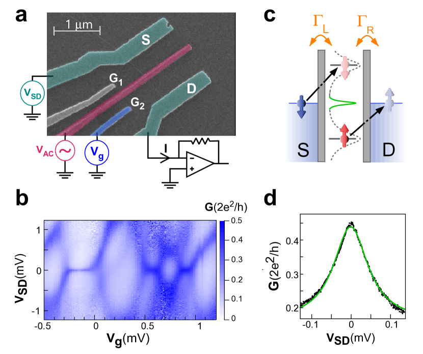
Our device is a carbon nanotube quantum dot circuit embedded in a coplanar waveguide microwave cavity (figure 1a). A bias voltage can be applied to one of the two Pd contact electrodes (emerald green). A DC gate voltage applied on a side gate electrode (blue) tunes the dot orbital energy. A central top gate electrode (pink) is used to apply a microwave signal to the device. Our calibration shows that although it is connected to the top gate electrode, it predominantly results in a source and drain AC bias voltage (see Appendix). Our setup measures the current I and the DC differential conductance at 20mK. Figure 1b shows a conductance color plot in absence of microwave excitation (). It displays zero-bias ridges characteristic of the Kondo regime. One of the Kondo resonance conductance peak (figure 1d) corresponds to a Kondo temperature extracted from a Lorentzian fit (see Appendix A). Note that typical Kondo temperatures in carbon nanotubes rather lie in the range, but a lower is advantageous to explore the Kondo dynamics in the relevant regime with accessible GHz frequencies.
III KONDO PEAK UNDER MICROWAVE IRRADIATION
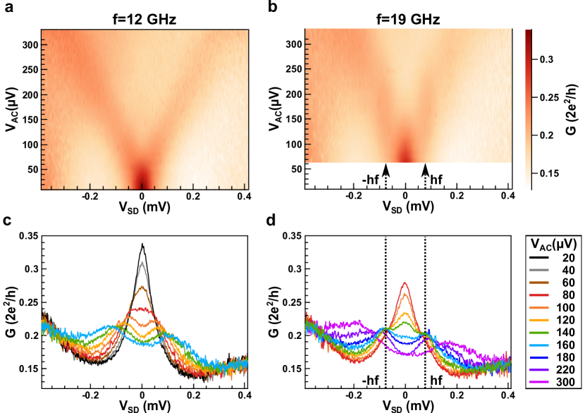
We now apply a finite microwave excitation and study how the Kondo resonance conductance peak is modified, for two excitation frequencies and for which the microwave excitation is dominantly coupled to the source-drain bias of the dot (see Appendix A). Our measurements confirm the phenomenology observed in previous experiments (figure 2). The strongest the microwave excitation, the lowest the Kondo resonance peak (figure 2c,d). Above a certain excitation voltage, several peaks are visible. For , we observe a linear splitting of the Kondo resonance versus (figure 2a,c), which corresponds to the adiabatic regime. In contrast, for , three peaks can be resolved simultaneously (green curve on figure 2d), and the two side peaks remain locked at over a certain range of excitation voltage (figure 2b,d). These satellites are the manifestation of photo-induced Kondo resonances. Figures 2c and 2d also show that the conductances at the Kondo resonance () with and without applied microwave excitation ( and ) clearly differ and that the variation of with quantitatively differs for and .
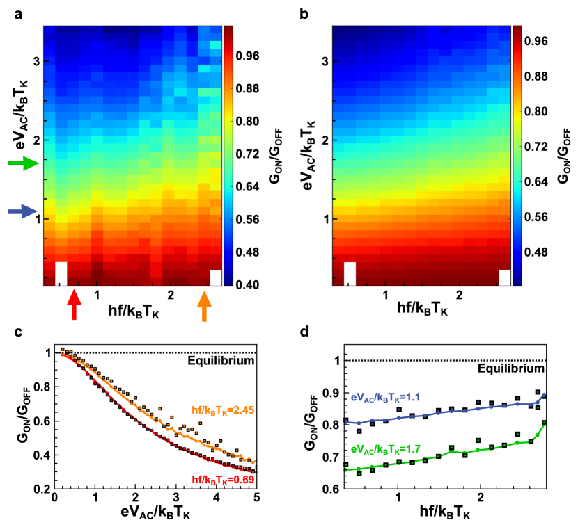
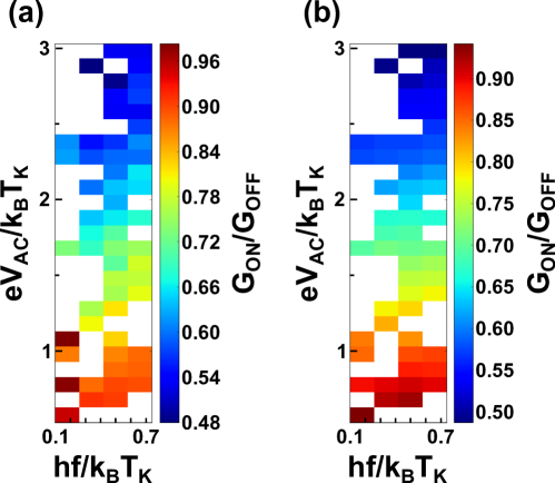
Using our calibration, we obtain the experimental map of the conductance ratio with and without microwave excitation as a function of the scaled amplitude and scaled frequency (figure 3a, see Appendix A). While decreases with , it increases with . These trends appear even more clearly on the map line cuts plotted in figure 3c and 3d. The higher the amplitude, the further the conductance at the Kondo resonance gets away from the equilibrium value, up to data noise. In contrast, the higher the frequency, the closer the Kondo conductance gets to its equilibrium value. Both behaviors were predicted by Kaminski, Nazarov and Glazman for an AC excitation of the bias voltage, in the limits and respectively. From their theoretical work, we build the following Ansatz to quantitatively describe our data for finite values of and :
| (1) |
with
| (2) |
where is a dimensionless parameter. More precisely, this expression bridges the analytical expressions of in the adiabatic limit (Eq.(76) of Ref.Kaminski2000 ) and in the low-amplitude high-frequency limit (Eq.(74) of Ref.Kaminski2000 ). Strikingly, our Ansatz is able to reproduce the full amplitude-frequency map of with a single adjustable parameter a=4.4 (figure 3b). A 10 global correction has been applied to amplitudes (), to account for absolute calibration uncertainty. The good agreement between our Ansatz and our measurements can be better appreciated from the linear cuts displayed in 3c and 3d.
Can we find a physical picture for the counter-intuitive frequency dependence we observe? Indeed one would rather think that higher frequencies would represent more energetic perturbations for the Kondo cloud, thus resulting in more decoherence. However, our AC excitation affects the phase difference between the electronic states in the source and drain electrodes, which becomesTien1963 for . These phase oscillations trigger inelastic cotunneling processes in which the dot spin is flipped and an electron is sent above the Fermi level of the reservoirs, so that the circuit gets out of the highly conducting many-body singlet Kondo ground state (see Figs.4a and d). The rate associated to this decoherence process depends on the amplitude of the phase oscillations, which vanish at high excitation frequencies due to the factor in the above equation (see Fig.4b). This simple fact explains that the Kondo cloud is less affected by higher frequencies. More quantitatively, at first order in , the two spin states of the dot are coupled by an oscillating matrix element with amplitude (see Eq.(18) of Ref.Kaminski2000 ), with the spin exchange factor of the Kondo hamiltonian in equilibrium. In the limit , which we consider for simplicity, decoherence is dominated by single photon absorption processes such as the one represented in 4a, and it involves initial reservoir states which must lie in a band of width below the Fermi energy of the leads, as visible from Fig.4a. Hence, from the Fermi’s golden rule, one gets with the density of states in the leads. Once the dot spin is flipped, its conductance is negligible in comparison with the unitary conductance of the Kondo limit. Since the circuit relaxes to the Kondo ground state with a rate , the average conductance reads , with , which corresponds to Eq.(74) of Ref.Kaminski2000 . This reasoning explains the increase of with but also agrees with the decrease of with .

IV SCALING LAWS
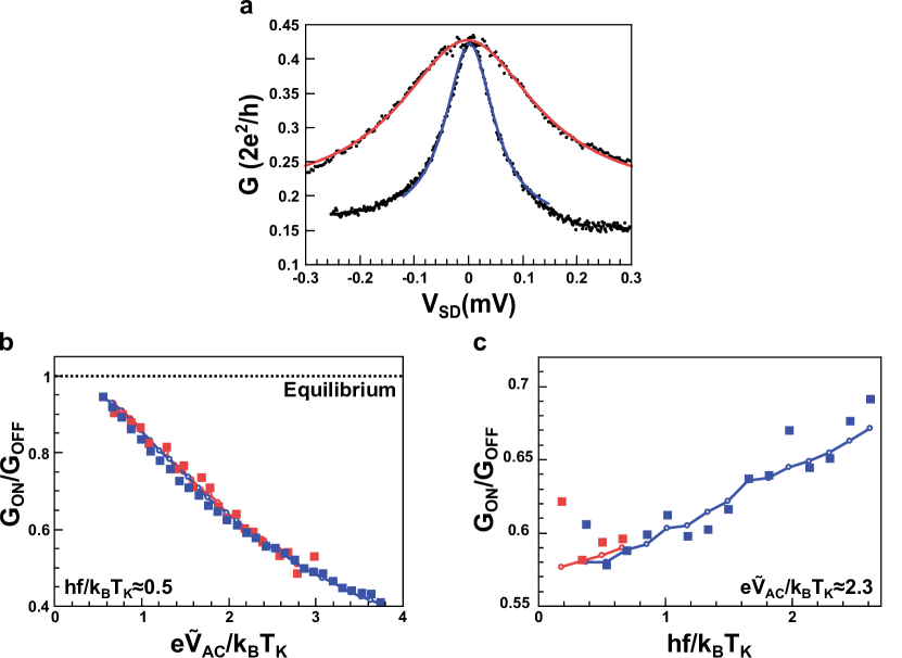
Finally, we investigate the crucial issue of the AC Kondo predicted universality properties. Is really governed by the reduced parameters and ? To address this question, we compare the AC response of Kondo resonances with significantly different Kondo temperatures. The peak fitted by the blue line in figure 5a is the ”narrow” Kondo resonance, where the frequency-amplitude characterization of previous section has been measured. The peak fitted by the pink line is three times broader and corresponds to . On the one hand, this factor 3 is advantageous, as scaling should be tested unambiguously. On the other hand, it also means that the investigated scaled frequency range is correspondingly reduced. Indeed our microwave source delivers up to 20GHz frequencies, so we are limited to . Following the color code of 5a, figure 5b (resp. 5c) shows on the same graph for the two peaks as a function of scaled amplitude (resp. scaled frequency) at fixed scaled frequency (resp. scaled amplitude ). By definition, the pink and blue Ansatz curves merge, up to small discrepancies due to noise in values. In figure 5b, experimental data for both narrow and broad Kondo peaks collapse well onto the Ansatz curve. This demonstrates the universal dependence of on at low frequency. In figure 5c, experimental data for the broad peak come down to four points, as explained above. They fall reasonably well on the narrow-peak data and confirm a flat adiabatic behavior at low scaled frequency. This is consistent with a universal frequency dependence, although universality in the pronounced frequency-dependant regime could not be investigated.
V CONCLUSION
Our experiment realized on a CNT-based quantum dot brings conclusions to several open issues of the AC Kondo problem. Using an independent in-situ amplitude calibration, we provide the first quantitative measurement of the amplitude-frequency dependence of the Kondo conductance with an AC bias. We observe or not Kondo side peaks, depending on the excitation frequency used. The Kondo resonance is found to be less affected at higher excitation frequencies, in agreement with Kaminski et al. Kaminski2000 . We describe our data quantitatively using an Ansatz, which bridges expressions given in this paper for two limiting regimes of parameters. Measurement on two Kondo resonances with very different allows to make tests of the universality of the Kondo behavior. We find a good scaling of with the scaled amplitude . In the more limited parameter range we could explore, our data is also consistent with a scaling of with the scaled frequency .
VI Acknowledgements
We thank Leonid Glazman for fruitful discussions. We gratefully acknowledge J. Palomo, M. Rosticher and A. Denis for technical support. The device has been made within the consortium Salle Blanche Paris Centre. This work is supported by ERC Starting Grant CirQys.
VII APPENDIX A: EXPERIMENTAL DETAILS
VII.1 Sample fabrication and measurement
Carbon nanotubes (CNTs) were
grown on a separate quartz substrate containing mesas and transferred onto a
high-resistivity / substrate using a method described in ref. Viennot2014a . After localizing CNTs with a Scanning Electron Microscope, the device
electrodes were patterned using electronic nanolithography. The two outer normal electrodes (70nm Pd) are connected to the
CNT with a room temperature resistance of . In contrast, the
central superconducting electrode (4nm Pd/100nm Al) is disconnected, and
acts as a top gate, on which we apply a microwave voltage to perform our
study of the AC Kondo. Transport measurements as a function of the two side
gates show parallel lines with a single slope, corresponding to a single dot
behaviour. Therefore a single side gate is operated with gate voltage . In addition to the DC current, the differential conductance G is measured
by synchronous detection using a small AC bias voltage of 10 at 77.77
Hz. The device is embedded in a Nb coplanar waveguide resonator, which was
not used in this work as transmission measurements showed no coupling
between the two systems.
VII.2 Fitting the Kondo resonance at equilibrium
We fit the Kondo resonance conductance peak in absence of microwave excitation by an offset Lorentzian curve (figures 1d and 5a) :
| (3) |
The Lorentzian peak is centered on with an amplitude and a
width setting our practical definition of . The parametrization is
chosen to recover the SU(2) coefficient of the (quadratic) Fermi liquid
description at low energy Glazman2003 . The presence of an offset
background conductance is commonly observed in the Kondo regime
Jarillo-Herrero2005 . For instance, this could be a contribution of
cotunnelling, which would evolve over the scale , which can be considered as flat over the Kondo resonance versus bias
voltage.
VII.3 Microwave amplitude calibration
Our in-situ calibration method consists in measuring the current rectification under microwave excitation in the Coulomb regime. Considering our parameter range ( and ), we can reasonably assume that the AC excitation simply modulates the DC current-voltage characteristic I(V). This leads to the following expression of the measured current :
| (4) |
which is expressed to lowest order in the excitation voltage on the sample . This is valid if explores the linear part of the
characteristic , leading to . For each
frequency a proportionality coefficient c(f) links the sample voltage to the
source voltage : . The c(f) values and the
detailed procedure to obtain them are given in the Appendix B
(figure 6). Note that equation 5 holds only if the microwave excitation
mainly acts as an AC bias voltage. This is the case of most excitation
frequencies, where the calibration coefficient c(f) is independent of the
gate voltage. Frequencies with a gate-dependent c(f) correspond to a mixed
AC bias-AC gate excitation regime, which is not the well controlled
situation we want to study. These frequencies are excluded from the
frequency set used for the AC Kondo characterization (for more details, see Appendix C and figure 7).
VII.4 Scaled frequency-amplitude conductance map building procedure
The experimental scaled frequency-amplitude conductance map shown in figure 3a (resp. in figure 9) is built from a database of 5189 sets (resp. 189) of (f, , G) gathering all measurements of the microwave response of the ”narrow” blue (resp. ”broad” pink) Kondo peak in figure 5a. The various measurement types and data extraction procedures are detailed in the Appendices. The amplitude calibration coefficients c(f) are used to calculate the excitation amplitude from . , and are obtained from the equilibrium Kondo resonance fit (see equation 3 above) before each data acquisition (see table in figure 8 for parameters). This allows to calculate the excitation scaled frequency and scaled amplitude . The conductance under excitation is obtained by subtracting the background conductance . We assume not being changed by the excitation, as . This assumption is validated by figure 2c,d, where conductance curves for all values merge at high bias voltage. For comparison between different data sets and/or between data and theory, it is relevant to normalize by the equilibrium conductance : . Finally, because data points are not uniformly spaced in - plane, we choose a regular grid and obtain the map matrix by averaging data points in the same cell. Cells with no data points remain blank. Here the cell size is 0.16 in and 0.1 in . The Ansatz scaled frequency-amplitude conductance maps are built following the same procedure except that the values for are calculated from the Ansatz formula 1 given in the main text, using experimental values for , and . This explains why the Ansatz curves are not perfectly smooth.
VIII Appendix B: In situ microwave amplitude calibration
Our in-situ calibration method consists in measuring the current rectification under microwave excitation in the Coulomb regime. Considering our parameter range ( and ), we can reasonably assume that the AC excitation simply modulates the DC current-voltage characteristic I(V). This leads to the following expression of the measured current :
| (5) |
which is expressed to lowest order in the excitation voltage on the sample . This is valid if explores the linear part of the characteristic , leading to . For each frequency a proportionality coefficient c(f) links the sample voltage to the source voltage : .
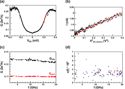
Two calibration methods were combined to obtain the values of c(f). The first method provides a reliable absolute calibration. In absence of excitation () is measured at on the side of a Coulomb diamond. This is the local slope of the conductance as a function of bias voltage near , as depicted on figure 6a. Figure 6b shows the current at as a function of . We focus on the low excitation regime, where the dependence is linear in agreement with 5. Knowing at , the slope gives access to c(f). Applying this method for each frequency is time-consuming and the sample working point may change between first and last measured frequencies. Relative calibration is performed more rapidly and reliably using a second method. The source voltage is fixed and the frequency is swept. Current is successively measured with (ON current ) and without (OFF current ) microwave excitation for each frequency point. For frequencies and with c(f) such, that the lowest-order expansion 5 is valid, calibration coefficients and are related by current rectification ratios :
| (6) |
Relative calibration can be refined by iterating the procedure. We apply a source voltage calculated to apply a constant excitation voltage . The new relative calibration is deduced from :
| (7) |
This relation holds replacing the current I by the differential conductance G. Figure 6c shows the conductance ON and OFF measurement, which defined the final relative calibration for some frequencies.
Figure 6d shows the coefficients c(f) used to calibrate the amplitude applied to the device for the study of the AC response of the narrow (blue dots) and broad (pink dots) Kondo peaks. Amplitude calibration for the narrow peak frequencies was done by combining absolute calibration and relative calibration methods described above. The resulting c(f) are on the same order of magnitude. This is because they have been preselected to be, otherwise relative powers may vary over tens of dB. We make this pre-selection to get a similar power range for all frequencies from the 43dB dynamic power range of our microwave source. For the broad Kondo peak, calibration was performed by iterating a relative calibration obtained on the narrow peak. Calibration coefficients differ between broad and narrow peaks because a thermal cycling occurred between the two measurements runs. The thermal cycling did not change the calibration coefficients order of magnitude, but relative calibration was modified, possibly because wire bonds moved. Note that figure 6d plots calibration coefficients only for frequencies kept after the frequency selection procedure, which we detail now.
IX APPENDIX C: Frequency selection procedure
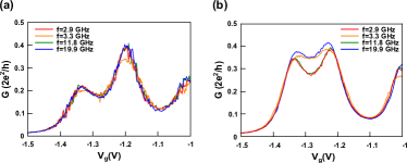
Once calibration is done, we study its gate dependence. We measure the conductance as a function of gate voltage successively with excitation ON () and OFF. This is done at finite bias for all calibrated frequencies. As expected the curves coincide at , where calibration was performed. We keep only frequencies, which curves superpose entirely. For example we observe on figure 7a that frequencies 2.9, 11.8 and 19.9 GHz match well at all gate voltages, while 3.3 GHz does not. As a result 3.3 GHz is excluded from the study of AC Kondo. Frequencies remaining after this procedure correspond to an AC excitation mainly applied on the dot bias voltage. When current rectification is gate-dependent, the AC excitation very likely also applies to the dot energy level. Kaminski et al Kaminski2000 predicted an opposite frequency-dependence of the AC Kondo conductance with this kind of coupling, compared to coupling to bias. is predicted to be decreasing with frequency instead of being increasing with frequency, as we measured. Figure 7b shows that the Kondo conductance at 3.3 GHz is higher than at 2.9 GHz and 11.8 GHz, which is consistent with microwaves partly coupling to the gate. However we chose not to study this mixed coupling regime, as it is not easy to quantify couplings to bias and to gate separately. Note that the thermal cycling between the measurement runs affected the coupling mode at some frequencies, possibly because wire bonds moved. In the post-processing of the narrow peak data set, 25 frequencies were excluded starting from 86 frequencies. For the broad peak, 22 frequencies out of 59 were excluded.
X APPENDIX D: From raw data to scaled and normalized data
The AC response of a narrow Kondo peak () was studied during a first measurement run. This corresponds to data files 0 to 6 ; 13 to 16 ; 18 and 19 in the table presented in figure 8. From these files 5189 sets of (f, , G) on the Kondo resonance have been extracted and used for the analysis. After a thermal cycling the sample displayed a broad Kondo peak (). 189 data points were extracted from files 9 and 12 and used in the analysis.
Data types are explicitly indicated by the file name. They are three fold. Grayscale f2-Vac are measurements on the Kondo resonance peak, where the frequency is the sweeping loop, while the excitation voltage is the incremental loop. GrayscaleVgf2OnOff are gate sweeps for different frequencies at constant , the RF power being successively switched ON and OFF between sweeps. Multigrayscale-VsdP2-f2 are three loops measurements with the excitation frequency as external loop, the excitation voltage or power as intermediate loop and the bias voltage as internal loop.

We detail below how , and have been determined for each measurement type. The parameter values are tabulated in the table of figure 8. They were used to scale the excitation amplitudes and frequencies and normalise the conductance as described in the Appendix A.
X.1 Grayscale f2-Vac
The Kondo resonance at equilibrium is measured and fitted by an offset Lorentzian to obtain , and (see Appendix A). and are fixed on the Kondo peak during the measurement as a function of excitation frequency and amplitude.
X.2 GrayscaleVgf2OnOff
For each gate sweep, we extract the locally minimal conductance value on the Kondo ridge. This allows us to extract the Kondo conductance with and without microwave excitation for each frequency. As the Kondo conductance without excitation shifts slightly over time, we assume that varies between sweeps, while is taken constant and is determined from fitting the Kondo resonance versus bias voltage without microwave excitation acquired before measuring GrayscaleVgf2OnOff.
X.3 Multigrayscale-VsdP2-f2
Here the equilibrium Kondo parameters are obtained for each frequency by fitting the conductance versus measured at the lowest excitation amplitude, provided that . This is justified by the observation that excitation amplitudes below this threshold do not affect the Kondo conductance compared to equilibrium. The conductance values on the Kondo peak are extracted by filtering the points with closest to the Lorentzian center fitting parameter . , and are calculated with the specific fitting parameters found for the corresponding frequency. Values tabulated in the table shown on figure 8 are averaged quantities, with standard deviation indicated in other columns.
XI APPENDIX E:Scaled amplitude-frequency conductance maps for the ”broad” Kondo peak
Figure 9 displays the experimental and Ansatz scaled amplitude-frequency normalized conductance maps for the broad Kondo peak. The higher number of blank cells compared to the ”narrow” peak maps is due to the lower number of data sets in the database from which the conductance matrix is built.
References
- (1) D. Goldhaber-Gordon, Hadas Shtrikman, D. Mahalu, D. Abusch-Magder, U. Meirav and M. A. Kastner, Kondo effect in a single-electron transistor, Nature 391, 156 (1998).
- (2) J. Nygård, D.H. Cobden and P.E. Lindelof, Kondo physics in carbon nanotubes, Nature 408, 342 (2000).
- (3) W.G. van der Wiel, S. De Franceschi, T. Fujisawa, J.M. Elzerman, S. Tarucha, L.P. Kouwenhoven, The Kondo effect in the unitary limit, Science 289, 2105 (2000).
- (4) Z. Iftikhar, S. Jezouin, A. Anthore, U. Gennser, F.D. Parmentier, A. Cavanna, F. Pierre, Two-channel Kondo effect and renormalization flow with macroscopic quantum charge states, Nature 526, 233 (2015).
- (5) A. J. Keller, L. Peeters, C. P. Moca, I. Weymann, D. Mahalu, V. Umansky, G. Zaránd, D. Goldhaber-GordonUniversal Fermi liquid crossover and quantum criticality in a mesoscopic system, Nature 526, 237 (2015).
- (6) M.M. Desjardins, J.J. Viennot, M.C. Dartiailh, L.E. Bruhat, M. Lee, M.-S. Choi, M.R. Delbecq, A. Cottet and T. Kontos Observation of the frozen charge of a Kondo resonance, Nature 545, 71 (2017).
- (7) T. Hensgens, T. Fujita, L. Janssen, X. Li, C. J. Van Diepen, C. Reichl, W. Wegscheider, S. Das Sarma, L. M. K. Vandersypen, Quantum simulation of a Fermi Hubbard model using a semiconductor quantum dot array, Nature 548, 70 (2017).
- (8) L. P. Kouwenhoven, S. Jauhar, J. Orenstein, P. L. McEuen, Y. Nagamune, J. Motohisa, and H. Sakaki, Observation of Photon-Assisted Tunneling through a Quantum Dot, Phys. Rev. Lett. 73, 3443 (1994).
- (9) W. G. van der Wiel, S. De Franceschi, J. M. Elzerman, T. Fujisawa, S. Tarucha, and L. P. Kouwenhoven, Electron transport through double quantum dots, Rev. Mod. Phys. 75, 1 (2003).
- (10) K. Shibata, A. Umeno, K.M. Cha and K. Hirakawa, Photon-assisted tunneling through self-assembled InAs quantum dots in the terahertz frequency range, Phys. Rev. Lett. 109, 077401 (2012).
- (11) R. Deblock, E. Onac, L. Gurevich and L.P. Kouwenhoven, Detection of Quantum Noise from an Electrically Driven Two-Level System, Science 301, 203 (2003).
- (12) E. Onac, F. Balestro, B. Trauzettel, C. F.J. Lodewijk and L.P. Kouwenhoven, Shot-noise detection in a carbon nanotube quantum dot, Phys. Rev. Lett. 96, 026803 (2006).
- (13) T.-K. Ng, AC Response in the Nonequilibrium Anderson Impurity Model, Phys. Rev. Lett. 76, 487 (1996).
- (14) J. König, H. Schoeller and G. Schön, Zero-Bias Anomalies and Boson-Assisted Tunneling Through Quantum Dots, Phys. Rev. Lett. 76, 1715 (1996).
- (15) A. Schiller and S. Hershfield, Solution of an AC Kondo Model, Phys. Rev. Lett. 77, 1821 (1996).
- (16) P. Nordlander, N.S. Wingreen, Y. Meir and D.C. Langreth, Kondo Physics in the Single Electron Transistor with ac Driving, Phys. Rev. B 61, 2146 (2000).
- (17) R. López, R. Aguado, G. Platero and C. Tejedor, Kondo Effect in ac Transport through Quantum Dots, Phys. Rev. Lett. 81, 4688 (1998).
- (18) Y. Goldin and Y. Avishai, Nonlinear Response of a Kondo System: Direct and Alternating Tunneling Currents, Phys. Rev. Lett. 81, 5394 (1998).
- (19) A. Kaminski, Y.V. Nazarov and L.I. Glazman, Suppression of the Kondo Effect in a Quantum Dot by External Irradiation, Phys. Rev. Lett. 83, 384 (1999).
- (20) A. Kaminski, Y.V. Nazarov and L.I. Glazman, Universality of the Kondo effect in a quantum dot out of equilibrium, Phys. Rev. B 62, 8154 (2000).
- (21) B. Béri and N. R. Cooper, Topological Kondo Effect with Majorana Fermions, Phys. Rev. Lett. 109, 156803 (2012).
- (22) J.M. Elzerman, S. De Franceschi, D. Goldhaber-Gordon, W.G. van der Wiel and L.P. Kouwenhoven, Suppression of the Kondo Effect in a Quantum Dot by Microwave Radiation, J. Low Temp. Phys. 118, 375 (2000).
- (23) A. Kogan, S. Amasha and M.A. Kastner, Photon-Induced Kondo Satellites in a Single-Electron Transistor, Science 304, 1293 (2004).
- (24) K. Yoshida, K. Shibata and K. Hirakawa, Terahertz Field Enhancement and Photon-Assisted Tunneling in Single-Molecule Transistors, Phys. Rev. Lett. 115, 138302 (2015).
- (25) P. W. Anderson, A poor man’s derivation of scaling laws for the Kondo problem, J. Phys. C 3, 2436 (1970).
- (26) B. Hemingway, S. Herbert, M. Melloch and A. Kogan, Dynamic response of a spin-1/2 Kondo singlet, Phys. Rev. B 90, 125151 (2014).
- (27) P.K. Tien and J.P. Gordon, Multiphoton process observed in the interaction of microwave fields with the tunneling between superconductor films. Phys. Rev. 129, 647 (1963).
- (28) J.J. Viennot, J. Palomo and T. Kontos, Stamping single wall nanotubes for circuit quantum electrodynamics Appl. Phys. Lett. 104, 113108 (2014).
- (29) L.I. Glazman and M. Pustilnik, Coulomb blockade and Kondo effect in quantum dots, eprint arxiv:0302159 (2003).
- (30) P. Jarillo-Herrero, J. Kong, H.S.J. Van Der Zant, C. Dekker, L.P. Kouwenhoven, S. De Franceschi, Orbital Kondo effect in carbon nanotubes Nature 434, 484 (2005).