SmB6: A material with anomalous energy distribution function of charge carriers?
Abstract
We argue that because of valence-fluctuation caused dynamical changes (fluctuations) of impurity energies in an impurity band of valence fluctuating semiconductors both occupied and unoccupied sites can be found in the impurity band above as well as below the Fermi level even in the ground state. As a consequence, the ground state energy distribution function of the subsystem of localized charge carriers for valence fluctuating semiconductors is qualitatively different than one for conventional semiconductors at K, what sheds new light on interpretation of experimental results of valence fluctuating semiconductors, e.g. SmB6 and YbB12, at lowest temperatures.
SmB6 is a prototypical mixed valence material revealing properties of a narrow-gap semiconductor down to few Kelvins Wachter93 ; Riseborough00 ; Allen79 ; Cooley95 ; Batko93 ; Gorshunov99 ; Batkova18PhB ; Stern17 ; Batkova18Jal ; Batkova06 . Paradoxically, at lowest temperatures its conductivity exhibits presence of a temperature non-activated term Wachter93 ; Riseborough00 ; Allen79 ; Cooley95 ; Batko93 ; Gorshunov99 ; Batkova18PhB ; Stern17 ; Batkova18Jal , which however, cannot be attributed to any scattering scenario known for metals, because very high value of corresponding residual resistivity would require superunitary scattering Wachter93 ; Riseborough00 ; Allen79 ; Cooley95 . According to Mott-Ioffe-Regel viewpoint, conventional Boltzmann transport theory becomes meaningless if the characteristic mean free path of the itinerant conduction electrons becomes comparable to, or less than the interatomic spacing Ioffe60 ; Mott71 , so the requirement for superunitary scattering implicates that either (i) electrical conductivity is not homogeneous in the volume, i.e. material contains metallic regions forming along the sample a conductive path responsible for electrical conductivity at lowest temperatures Dzero10 ; Dzero12 ; Lu13 ; Alexandrov13 ; Zhu13 or (ii) electrical transport at lowest temperatures is realized via a hopping-type transport that in contrast to one in conventional semiconductors has to be temperature non-activated BaBa14 .
The first mentioned approach supposes metallic surface of SmB6 which can be either of topological nature Dzero10 ; Dzero12 ; Lu13 ; Alexandrov13 or due to ”trivial” polarity-driven surface states Zhu13 . Indeed, many experimental observations indicate metallic surface transport in (stoichiometric) SmB6 Wolgast13 ; Kim13 ; Syers15 . On the other hand, Raman scattering studies Valentine16 showed that presence of even 1 % of Sm vacancies leads to smearing of the bulk hybridization gap in this material (being in qualitative agreement with earlier theoretical predictions Riseborough03 ), and would result in a breakdown of the topological Kondo insulator state Valentine16 . Other studies of vacant samples Sm1-xB6, for ranging from to , revealed resistivity saturation at lowest temperatures Gabani16 similar to that of the stoichiometric SmB6. Because concentration of Sm vacancies in these samples substantially exceeds level of 1 %, topologically protected surface states should not be present here, what implicates that scenario of topological Kondo insulator is not applicable in the case of all Sm-vacant samples.
The second above mentioned approach is represented by the scenario of valence-fluctuation induced hopping transport BaBa14 that is applicable also to vacant SmB6-based samples. The key assumptions of this scenario, namely (i) presence of valence fluctuations (VFs), (ii) existence of an impurity band (IB), and (iii) the Fermi level lying in the IB, are in agreement with theoretical studies of impurity states in mixed-valent materials Schlottman92 ; Schlottman96 ; Riseborough03 , studies of electrodynamic properties of SmB6 in the low-frequency regime Gorshunov99 , optical conductivity studies of SmB6 Laurita16 ; Laurita18 , observation of presence of variable-range hopping transport in SmB6 at lowest temperatures Batkova18PhB , and many other experimental observations reported for SmB6 (see e.g. Gorshunov99 ; Laurita16 ; Laurita18 ; Demishev18 and references therein). As explained in BaBa14 , the energy of an impurity in the semiconductor with an IB that contains metallic ions in two different valency states (e.g. and ) depends on the distribution of ion valences in the vicinity of this impurity (because of different interaction energy of this impurity with ions of different valency due to their different charge, ionic radii, and magnetic moment). Changes in distribution of ion valences unconditionally cause corresponding changes of the impurity energies and can be modeled by a rearrangement process (RP) with a characteristic time constant, BaBa14 . Thus, the energy of the impurity is not constant in time, but varies within some interval BaBa14 . Therefore, if the Fermi level, , lies in the IB, there has to exist a subnetwork of impurities for which it is true that due to the RP some occupied impurity energy levels can shift from the region below to the region above , and analogously, some empty levels from the region above can shift under . This not only creates favorable conditions for temperature non-activated hops that are responsible for temperature non-activated transport BaBa14 , but also causes a change of energy distribution function (EDF) of charge carriers. It is the purpose of this work to point out that the EDF of localized charge carriers in the ground state of valence fluctuating semiconductors qualitatively differs from one expected for conventional semiconductors at K, and that the absence of low temperature resistivity divergence in (real) SmB6-based samples containing lattice imperfections can be a natural consequence of the changed EDF.
According to the “quantum-limit” hopping formula Ambegaokar71 , the intrinsic transition rate for an electron hopping from a site with energy to an empty site with energy in the simplest case, when is of the order of the Debye energy or smaller, and is small compared to , can be expressed as
| (1) | |||
| (2) |
where is Boltzmann constant, is the distance between sites and , and is a constant, which depends on the electron-phonon coupling strength, the phonon density of states, and other properties of the material, but which depends only weakly on the energies and or on Ambegaokar71 . According to Eq. (2), the intrinsic transition rate of electron hop to a site of less energy decreases exponentially with increasing . However, because is finite, must be also finite, so there is always non-zero time interval until an electron can hop (tunnel) to some empty site of less energy, while this time interval increases with increasing distance between the sites. If the RP (e.g. represented by VFs) is the ground state property of a material, finite suggests a non-zero probability of finding some occupied energy levels above also in the ground state. In a conventional semiconductor (i.e. one without the RP) the time averaged occupation number of site in the thermal equilibrium (at neglecting electron-electron interactions except those causing that not more than one electron can occupy a single site) can be expressed in the form Ambegaokar71 , what for K unconditionally means that all energy levels below are occupied and all energy levels above are empty. Thus, the above mentioned non-zero probability to find occupied energy levels above in the ground state implies that the ground-state EDF of the subsystem of localized charge carriers in materials with the RP is qualitatively different from the EDF in conventional semiconductors at K. This fundamental conclusion we support by the following discussion.
According to the scenario of valence-fluctuation induced hopping transport BaBa14 , a hopping site can be characterized by an energy interval of the typical width and by the partial DOS, , which is non-zero and constant within the interval and zero outside it (see Fig. 1a). Let us moreover characterize the site by a time averaged probability of the occupation of this site by an electron, . Because time interval until the electron can hop (tunnel) to an empty site of less energy increases with increasing distance between the sites, at very low concentration of impurities, or in case of the RP with a very short (e.g. fast valence fluctuating process), it can be reasonably considered that . This limit case practically means that electron occupies the state for sufficiently long time to receive any energy from the interval . We define the time averaged probability of the occupation of site by an electron, , as the average value of the Fermi-Dirac distribution function (FDDF), , over the energy interval . Assuming that all energy intervals have the typical width (i.e. ), can be expressed in the form
| (3) |
where . Fig. 1b shows as defined by Eq. (3) calculated for K and for fixed parameter .

As can be seen, for , for , and decreases linearly from 1 to 0 for in the interval . According to the above mentioned, all impurity sites having in the energy interval are overlapped at energy , and contribute to the probability of occupation of the state at energy proportionally to . Thus we can determine the time averaged probability of occupation of the state at energy in the IB (i.e. the EDF) as
| (4) |
Analytical calculation of Eq. 4 for K and for fixed gives
| (5) |
| (6) |
| (7) |
| (8) |
as depicted in Fig. 1c. As follows from Eqs. (5-8), the K is a continuous function with the finite slope K at the Fermi level. This represents a qualitaive difference in comparison with FDDF, since at (giving infinite slope for K). Considering that the slope of the EDF at reflects energy broadening (either due to a non-zero temperature or due to the RP), both slopes can be compared yielding
| (9) |
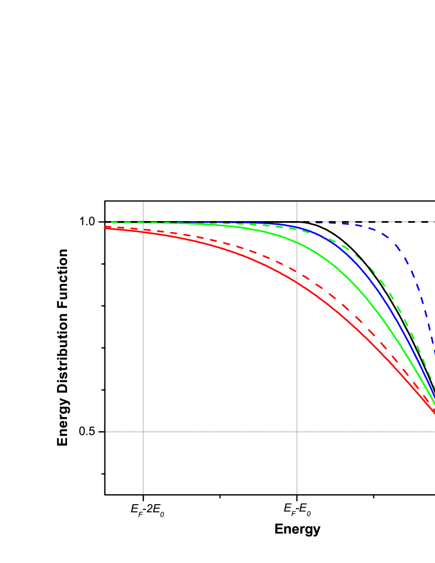
Fig. 2 shows numerically calculated plots of for K, , and compared with FDDFs calculated for the same temperatures. As can be seen, for K strongly differs from the FDDF at K, and can be much better approximated by the FDDF at the finite temperature . As can be deduced from the plots for , the EDF of the system with the RP can be at sufficiently low temperatures much better approximated by the FDDF at than by the FDDF at real temperature of the system. Thus it seems that the RP at lowest temperatures affects the EDF analogously as temperature enhanced to the value of . In general, all curves have less (negative) slope at in comparison with the slope of the FDDF (at ) at the same temperature, resembling the effect of a temperature enhancement due to the RP.
We suppose that the energy broadening as discussed above (for ) can be adopted also to the case of SmB6 because of the fast valence fluctuation rates in this material Mock86 . Deducing from Eqs. (5-8) and Fig. 2, at sufficiently high temperatures (where is much less than thermal broadening) the EDF of localized charge carriers in SmB6 will be practically unaffected by valence fluctuations (VFs). Approaching temperatures the EDF will exhibit essential deviation from the FDDF due to VFs, while at temperatures the EDF will resemble the FDDF corresponding to significantly greater temperature, . Consequently, physical characteristics of SmB6 that are governed by the EDF (e.g. electrical resistivity) will for K converge to those expected at a non-zero temperature, providing another reason for the absence of the resistivity divergence.
Here we would like to pay attention to some possible new phenomena which could take place at temperatures around and below . As follows from the definition (Eq. 4), is the function of parameter , thus affects the energy of the subsystem of localized charge carriers. At the same time, reflects a ”magnitude” of impurity energy fluctuation due to fluctuation of the properties of the surrounding lattice (because of VFs). Thus, can represent a ”driving force” to minimize the total energy of the system. For instance, ”tuning” of the processes associated with VFs (e.g. reasonable change of fluctuations in magnetic subsystem and the associated magnetic interactions/correlations) can yield such value of that the total energy will be minimized. Although at high temperatures () will practically not affect the , the influence of can become essential approaching temperatures close to , and it may appear as favorable to change physical state of the system such way that the total energy will be minimized due to changed interactions and correspondingly changed value of . No clear conclusion can be done here whether eventual change of should be continuous in a certain temperature interval or ”sudden”, resembling a phase transition. Nevertheless in can be still expected that such change of will be associated with change of physical properties of the system in a certain temperature region. As possible (or perhaps accidental) analogy with the above provided picture we would like to mention very recent ESR studies of SmB6 Demishev18 . The ESR signal observed at K was not more observed at K Demishev18 ; moreover, the critical behavior of the integrated ESR intensity, , with characteristic temperature K and exponent was observed, and the authors Demishev18 mentioned a possibility of ”some abrupt structural/magnetic transition” to explain experimental results and emphasized the importance of re-considering ”5 K anomaly” in context of modern topological physics of SmB6.
Finally, we would like to emphasize that presented results enable to explain absence of resistivity divergence at lowest temperatures in both stoichiometric, as well as in vacant SmB6 samples. The scenario of valence-fluctuation induced hopping transport BaBa14 and its consequences discussed here shed new light onto observations associated with ”5 K anomaly” by inferring possible existence of new phenomena ”driven” by the subsystem of localized charge carriers, while all these phenomena can be considered simultaneously with possible presence of topologically protected or/and polarity-driven metallic surface states in SmB6. We believe that our findings not only represent a base for understanding the underlying physics in valence fluctuating semiconducting compounds at lowest temperatures, but that they also indicate a necessity to consider similar phenomena in many other materials with ”dynamical ground state”, especially those obeying physical properties which cannot be adequately understood presumably supposing the ground state being associated with the FDDF for absolute zero.
This work was supported by the Slovak Scientific Agency VEGA (Grant No. 2/0015/17) and by the Slovak Research and Development Agency (APVV-15-0115).
References
- (1) P. Wachter. Handbook on the Physics and Chemistry of Rare Earths, volume 19. North Holland, 1993.
- (2) Peter S. Riseborough. Heavy fermion semiconductors. Advances in Physics, 49:257, 2000.
- (3) J. W. Allen, B. Batlogg, and P. Wachter. Large low-temperature Hall effect and resistivity in mixed-valent SmB6. Phys. Rev. B, 20:4807–4813, Dec 1979.
- (4) J. C. Cooley, M. C. Aronson, Z. Fisk, and P. C. Canfield. SmB6: Kondo insulator or exotic metal? Phys. Rev. Lett., 74:1629 – 1632, 1995.
- (5) I. Bat’ko, P. Farkašovský, K. Flachbart, E. S. Konovalova, and Yu. B. Paderno. Low temperature resistivity of valence fluctuation compound SmB6. Solid State Commun., 88:405 – 410, 1993.
- (6) B. Gorshunov, N. Sluchanko, A. Volkov, M. Dressel, G. Knebel, A. Loidl, and S. Kunii. Low-energy electrodynamics of SmB6. Phys. Rev. B, 59:1808–1814, Jan 1999.
- (7) M. Batkova, I. Batko, S. Gabáni, E. Gažo, E. Konovalova, and V. Filippov. Low temperature resistivity studies of SmB6: Observation of two-dimensional variable-range hopping conductivity. Physica B, 536:200–202, 2018.
- (8) A. Stern, M. Dzero, V. M. Galitski, Z. Fisk, and J. Xia. Surface-dominated conduction up to 240 k in the Kondo insulator SmB6 under strain. Nature Materials, 16:708 – 711, 2017.
-
(9)
M. Batkova, I. Batko, F. Stobiecki, B. Szymańskiand P. Kuświk,
A. Macková, and P. Malinský.
Electrical properties of SmB6 thin films
prepared by pulsed laser deposition from a stoichiometric SmB6 target. J. Alloys Compd., 744:821–827, 2018. - (10) M. Batkova, I. Batko, E. S. Konovalova, N. Shitsevalova, and Y. Paderno. Gap properties of SmB6 and YbB12: Electrical resistivity and tunnelling spectroscopy studies. Physica B, 378 - 380:618, 2006.
- (11) A.F. Ioffe and A.R. Regel. Non-crystalline, amorphous, and liquid electronic semiconductors. Progress in Semiconductors, page 237, 1960.
- (12) N.F. Mott and E. Davis. Electronic Processes in Non-Crystalline Materials. Clarendon Press, 1971.
- (13) Maxim Dzero, Kai Sun, Victor Galitski, and Piers Coleman. Topological Kondo insulators. Phys. Rev. Lett., 104:106408, Mar 2010.
- (14) Maxim Dzero, Kai Sun, Piers Coleman, and Victor Galitski. Theory of topological Kondo insulators. Phys. Rev. B, 85:045130, Jan 2012.
- (15) Feng Lu, JianZhou Zhao, Hongming Weng, Zhong Fang, and Xi Dai. Correlated topological insulators with mixed valence. Phys. Rev. Lett., 110:096401, Feb 2013.
- (16) Victor Alexandrov, Maxim Dzero, and Piers Coleman. Cubic topological Kondo insulators. Phys. Rev. Lett., 111:226403, Nov 2013.
- (17) Z.-H. Zhu, A. Nicolaou, G. Levy, N. P. Butch, P. Syers, X. F. Wang, J. Paglione, G. A. Sawatzky, I. S. Elfimov, and A. Damascelli. Polarity-driven surface metallicity in SmB6. Phys. Rev. Lett., 111:216402, Nov 2013.
- (18) I. Batko and M. Batkova. SmB6: Topological insulator or semiconductor with valence-fluctuation induced hopping transport? Solid State Commun., 196:18, 2014.
- (19) Steven Wolgast, Cagylian Kurdak, Kai Sun, J. W. Allen, Dae-Jeong Kim, and Zachary Fisk. Low-temperature surface conduction in the Kondo insulator SmB6. Phys. Rev. B, 88:180405, Nov 2013.
- (20) D. J. Kim, S. Thomas, T. Grant, J. Botimer, Z. Fisk, and Jing Xia. Surface Hall effect and nonlocal transport in SmB6: Evidence for surface conduction. Scientific Reports, 3:1, 2013.
- (21) Paul Syers, Dohun Kim, Michael S. Fuhrer, and Johnpierre Paglione. Tuning bulk and surface conduction in the proposed topological Kondo insulator SmB6. Phys. Rev. Lett., 114:096601, Mar 2015.
- (22) Michael E. Valentine, Seyed Koohpayeh, W. Adam Phelan, Tyrel M. McQueen, Priscila F. S. Rosa, Zachary Fisk, and Natalia Drichko. Breakdown of the kondo insulating state in by introducing sm vacancies. Phys. Rev. B, 94:075102, Aug 2016.
- (23) Peter S. Riseborough. Collapse of the coherence gap in Kondo semiconductors. Phys. Rev. B, 68:235213, 2003.
- (24) S. Gabáni, M. Orendáč, G. Pristáš, E. Gažo, P. Diko, S. Piovarči, V. Glushkov, N. Sluchanko, A. Levchenko, N. Shitsevalova, and K. Flachbart. Transport properties of variously doped SmB6. Philosophical Magazine, 96(31):3274–3283, 2016.
- (25) P. Schlottmann. Impurity bands in Kondo insulators. Phys. Rev. B, 46:998, 1992.
- (26) P. Schlottmann. Influence of a Kondo-hole impurity band on magnetic instabilities in Kondo insulators. Phys. Rev. B, 54:12324, 1996.
- (27) N.J. Laurita, C.M. Morris, S.M. Koohpayeh, P.F.S. Rosa, W.A. Phelan, Z. Fisk, T.M. McQueen, and N.P. Armitage. Anomalous three-dimensional bulk ac conduction within the Kondo gap of SmB6 single crystals. Phys. Rev. B, 94:165154, 2016.
- (28) N.J. Laurita, C.M. Morris, S.M. Koohpayeh, W.A. Phelan, T.M. McQueen, and N.P. Armitage. Impurities or a neutral Fermi surface? A further examination of the low-energy ac optical conductivity of SmB6. Physica B, 536:78–84, 2018.
- (29) S. V. Demishev, M. I. Gilmanov, A. N. Samarin, A. V. Semeno, N. E. Sluchanko, N. A. Samarin, A. V. Bogach, N. Yu. Shitsevalova, V. B. Filipov, M. S. Karasev, and V. V. Glushkov. Magnetic resonance probing of ground state in the mixed valence correlated topological insulator SmB6. Scientific Reports, 8:7125, 2018.
- (30) Vinay Ambegaokar, B. I. Halperin, and J. S. Langer. Hopping conductivity in disordered systems. Phys. Rev. B, 4:2612–2620, Oct 1971.
- (31) R. Mock, E. Zirngiebl, B. Hillebrands, G. Güntherodt, and F. Holtzberg. Experimental identification of charge relaxation rates in intermediate-valence compounds by phonon spectroscopy. Phys. Rev. Lett., 57:1040–1043, Aug 1986.