Equilibration of Quantum hall edges in symmetry broken bilayer graphene
Abstract
Equilibration of quantum Hall edges is studied in a high quality dual gated bilayer graphene device in both unipolar and bipolar regime when all the degeneracies of the zero energy Landau level are completely lifted. We find that in the unipolar regime when the filling factor under the top gate region is higher than the back gate filling factor, the equilibration is partial based on their spin polarization. However, the complete mixing of the edge states is observed in the bipolar regime irrespective of their spin configurations due to the Landau level collapsing at the sharp pn junction in our thin hBN ( 15 nm) encapsulated device, in consistent with the existing theory.
I Introduction
Since the discovery of fractional quantum Hall (QH) effect in two-dimensional electron gas there have been extensive research on the equilibration of edge states to understand their propertiesKane et al. (1994); Kane and Fisher (1997); Bid et al. (2010).Graphene, a single atomic layer of carbons, presents an unique platform where the equilibration of edge states along the pn junction gives rise to fractional values of conductance even in the integer QH regimeWilliams et al. (2007); Özyilmaz et al. (2007); Liu et al. (2008); Lohmann et al. (2009); Velasco Jr et al. (2009); Ki and Lee (2009); Ki et al. (2010); Velasco Jr et al. (2010); Jing et al. (2010); Woszczyna et al. (2011); Nam et al. (2011); Velasco et al. (2012); Bhat et al. (2012); Schmidt et al. (2013); Klimov et al. (2015); Morikawa et al. (2015); Kumada et al. (2015); Matsuo et al. (2015); Kumar et al. (2017). This is possible because the conduction and valance bands touch each other at the Dirac point, thus selective and control doping combined with the chiral nature of charge carriers can have co-propagating edge states along the pn junction interface. This co-propagating edge states has been used recently to demonstrate the mach zehnder interferometer in grapheneWei et al. (2017), where the selective equilibration between the symmetry broken QH edges determines the visibility of the interferometer.
Equilibration of edge states have been studied extensively Williams et al. (2007); Özyilmaz et al. (2007); Liu et al. (2008); Lohmann et al. (2009); Velasco Jr et al. (2009); Ki and Lee (2009); Ki et al. (2010); Velasco Jr et al. (2010); Jing et al. (2010); Woszczyna et al. (2011); Nam et al. (2011); Velasco et al. (2012); Bhat et al. (2012); Schmidt et al. (2013); Klimov et al. (2015); Morikawa et al. (2015); Kumada et al. (2015); Matsuo et al. (2015); Kumar et al. (2017) in graphene in both unipolar and bipolar regimes. The conductance plateaus observed are in agreement with the theoretical prediction by Abanin et al.Abanin and Levitov (2007). However, the conductance values in the unipolar regime for broken symmetry states in graphene device deviates from the predicted equilibration values Abanin and Levitov (2007) and were found to be in good match with the partial equilibration based on spin polarized edge statesAmet et al. (2014). Similar to graphene, the experiments are also performed on bilayer graphene (BLG), which has even more symmetries like orbital symmetry together with spin and valley symmetries. This leads to more complex Landau level (LL) phase diagram in BLG, which can be controlled independently by density, electric field and magnetic fieldLee et al. (2014); Kou et al. (2014); Maher et al. (2014); LeRoy and Yankowitz (2014); Hunt et al. (2017); Zibrov et al. (2017). The equilibration experiments performed in BLGJing et al. (2010) also echo with the theory Abanin and Levitov (2007). However, no equilibration study has been performed on the broken symmetry states of ultra clean BLG devices either in unipolar or bipolar regime.
In this article, we report on the equilibration of QH edge states in a high quality dual gated bilayer graphene device in both unipolar (n-n∗-n/p-p∗-p) and bipolar (n-p-n/p-n-p) regime when all the degeneracy of the zero-energy LL is lifted. We find that in the unipolar regime when the top gate filling factor () is higher than the back gate filling factor (), the conductance values does not follow the full equilibration predictionAbanin and Levitov (2007). Rather, they follow partial equilibrationAmet et al. (2014) based on the hierarchical splittingZibrov et al. (2017); Hunt et al. (2017) of zero energy LL with different spin configuration. Although the partial equilibration based on spin polarization is able to explain most of the conductance values in the unipolar regime but still it is unable to capture the conductance value for all the edge states. The lack of equilibration is better understood by considering the predominant mixing between the nearest edge states. Moreover, in the bipolar regime we find full equilibration of QH edge states for all combination of and irrespective of their spin configurations. The equilibration in the bipolar regime is understood in terms of LL collapsing at the sharp pn junction as predicted by Lukose et al.Lukose et al. (2007), NMR Peres et al. Peres and Castro (2007), Gu et al.Gu et al. (2011) and LaGasse et al.LaGasse and Lee (2016).
II Device Fabrication and Characterization
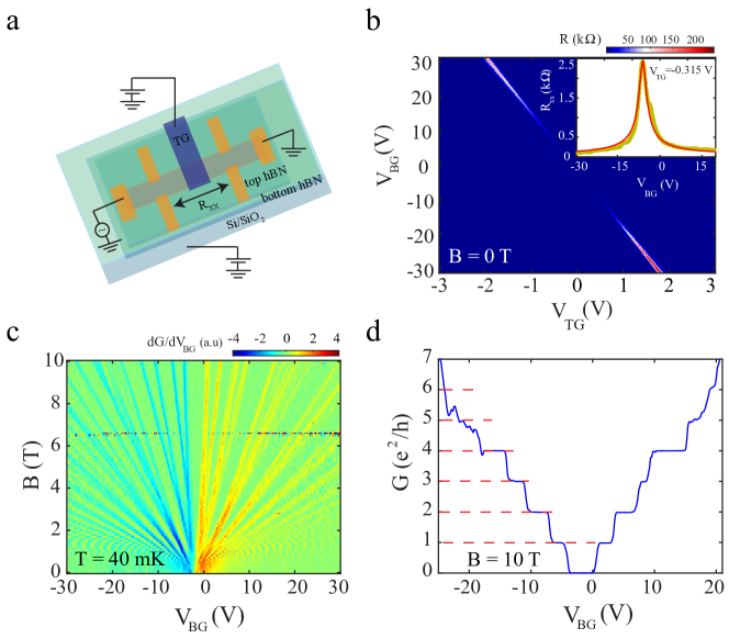
The bilayer graphene device is prepared using the dry transfer pick up techniqueWang et al. (2013) using following steps. First, a glass slide is prepared with a layer of pdms and ppc. This glass slide is used to pick up the desired hBN ( nm) flake, which is exfoliated on silicon wafer. On a separate silicon wafer graphite flakes are exfoliated and a bilayer graphene flake is picked up using the glass slide containing the pdms, ppc and hBN. The glass slide containing the heterostructure of pdms/ppc/hBN/BLG is then transfered on a thick hBN () which was already exfoliated on a separate silicon wafer. With this technique graphene remains in its pristine form as it is not exposed to any environmental contaminants or the pmma. The prepared stack of hBN/BLG/hBN is then cleaned in chloroform followed by acetone and IPA cleaning. Using the standard lithography technique the contacts are fabricated followed by etching in \chCHF3 and \chO2 environment. The etch rate is optimized to be 30 nm per minute. Soon after etching Cr(3 nm)/Pd(8 nm)/Au(70 nm) is deposited at a base pressure of 3e-7 mbar. The top gate is fabricated by doing another lithography on the prepared stack of hBN/Gr/hBN. The top gate acts as a local gate and controls the density only in the middle portion of the device while the thick \chSiO2 acts as a global back gate, controlling the density throughout the device as shown schematically in Fig. 1a, where the contacts are shown in yellow color and top gate is shown in blue color. The device is 5 long, 2 wide and the separation between inner contacts is 2.5 .
The conductance is measured using standard lock in technique. The different combination of back gate () and top gate () voltages leads to the formation of n-p-n/p-n-p or n-n∗-n/p-p∗-p region in the same device as shown in Fig. 1b. The diagonal line in Fig. 1b corresponds to the Dirac point under the top gated region, where the density is controlled by both and . From the slope of diagonal line we calculate top hBN thickness of nm. The inset shows resistance measured as a function of for V and from the fitting we obtain a mobility of . Figure 1c displays landau level fan diagram () as a function of and magnetic field (B) at V. Figure 1d shows the two probe conductance at T, where one can clearly see the QH plateaus at integer multiple of suggesting the lifting of spin, valley and orbital degeneracy of the zero energy LL of BLG.
III Equilibration of QH edges
Two probe conductance in the QH regime depends on the back gate () and top gate () filling factors. This is shown schematically in Fig. 2. The unipolar regime (i.e top gate and back gate region has same kind of charge carrier) is shown in Fig. 2a-c. When , then the current injected from the back gate region completely transmits through the top gate region without any back scattering. For , the extra edge states in the back gate region ( ) gets reflected back as shown in Fig. 2b. Hence, the conductance is determined only by the number of edge states under the top gate region and thus, the total conductance is given by
| (1) |
More interesting situation arises when . In this case edge channels are completely transmitted through the top gate region while number of edges keep circulating under the top gate region. The edge states transmitting through the top gate region can mix with the circulating channels under the top gate region, which leads to the modification of two probe conductance. In the case of complete mixing, which has been observed Williams et al. (2007); Özyilmaz et al. (2007); Liu et al. (2008); Lohmann et al. (2009); Velasco Jr et al. (2009); Ki and Lee (2009); Ki et al. (2010); Velasco Jr et al. (2010); Jing et al. (2010); Woszczyna et al. (2011); Nam et al. (2011); Velasco et al. (2012); Bhat et al. (2012); Schmidt et al. (2013); Klimov et al. (2015); Morikawa et al. (2015); Kumada et al. (2015); Matsuo et al. (2015); Kumar et al. (2017) on \chSiO2 substrate and the conductance is given as:
| (2) |
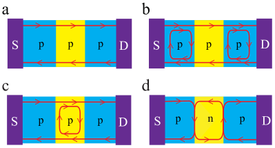
Another interesting scenario arises if the charge carrier in the top gate and the back gate region are of different type; holes and electrons. Since electron and hole has opposite chirality, the net two probe conductance will be zero unless the clock wise moving QH edge states can equilibrate with the anti-clock wise moving edge states along the pn junction interface as shown in Fig. 2d. For the complete equilibration case the two probe conductance is given as:
| (3) |
The conductance values discussed so far corresponds to the cases when the degeneracy like spin, valley or orbital are not lifted. Recent experimentAmet et al. (2014) by Amet et al. studies the equilibration (unipolar regime) in graphene when both the valley and spin degeneracies are completely lifted. In such scenario they have showed that the equilibration depends strongly on the spin configuration of the edge states. If the transmitting edge states () and inner circulating edge states under the top gate region (Fig. 2c) have opposite spin then the edge state do not equilibrate and hence the conductance is given by , on the contrary if the edge states have same spin, they equilibrate completely and conductance is given by Eq. 2. Thus, the conductance for spin polarized edge state in the unipolar regime can be given asAmet et al. (2014):
| (4) |
Here, refers to the total number of edge states with , same convention holds for . For example, if with and with and , then . On the other hand, if with and then .
IV Results
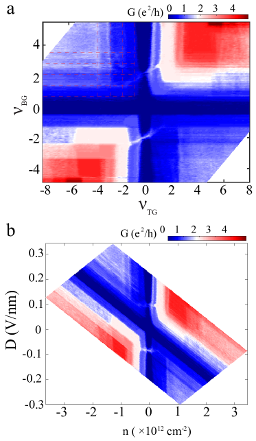
The color plot of two probe conductance as a function of and at 10 T is shown in Fig. 3a. The Fig. 3a is obtained from Fig. 1 of the SI, where the conductance is measured as a function of and at 10 T. The back gate and top gate voltages is converted to back gate and top gate filling factors, respectively, using , where is the density in the system, is the planks constant, is the electronic charge and is the applied magnetic field. The horizontal and vertical strips in Fig. 3a corresponds to different and , respectively. Interestingly, in the unipolar regime, for conductance remains constant at a value of from to . We also observe a similar feature for , where quantized conductance of is observed from to . On the other hand in the bipolar regime we observe a clear chequerboard pattern with the conductance values (Table I) expected for the full equilibration case (Eq. 3). Two lines of higher conductance are also observed connecting the unipolar and bipolar region. Note that these lines are placed symmetrically about . Fig. 3b shows color plot of conductance as a function of density () and displacement field (). The net density () and the displacement field () are obtained using following relationZhang et al. (2009):
and .
Here and are the applied back gate and top gate displacement
field, receptively. They are given as
and where () are the thickness of dielectric layers, () are the dielectric constants and () is the charge neutrality points (CNP) of the device. The high conductance line joining and LLs Lee et al. (2014); Kou et al. (2014); Maher et al. (2014); LeRoy and Yankowitz (2014); Hunt et al. (2017); Zibrov et al. (2017) is at .
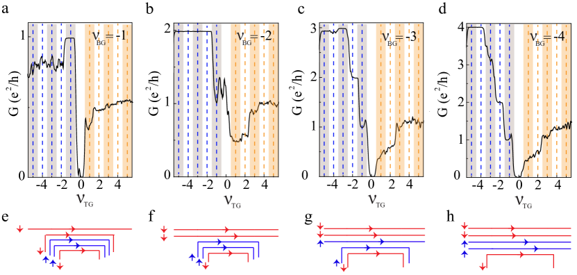
Figure 4a-d plots the cut lines obtained from Fig. 3a at different . In the unipolar regime expected quantized plateaus are observed for . For also the conductance plateaus agrees with Eq. 1 as can be seen in Fig. 4c and 4d. However, For the conductance plateaus is not consistent with full equilibration prediction as mentioned in Eq. 2. In-fact for the conductance plateau remains at from to . Similarly, Fig. 4d shows a plateau of from to for . For the full equilibration of QH edge states the conductance values of for was expected for and a value of for . This gives a very clear signature that some of the edge states, in particular prefer not to equilibrate with the circulating edges under the top gate region. Even for and (Fig. 4a and Fig. 4c) the conductance values obtained in the unipolar regime is higher than the full equilibration prediction. Similar behavior is also observed in the four probe resistance measurement(SI). However, in the bipolar region full equilibration of edge states are observed. Although the data in the bipolar regime do not show good plateau as observed in our previous work on single layer grapheneKumar et al. (2017) but its average value matches with Eq. 3. The measured conductance values in both unipolar and bipolar regimes have been compared with the theoretical prediction based on full equilibration shown in Table I. Each round bracket in Table I, from left to right lists the conductance value obtained using full equilibration followed by experimental value. The large mismatch of conductance observed in the unipolar regime between the theory and experiment is highlighted by dashed square.
| -1 | -2 | -3 | -4 | -5 | |
|---|---|---|---|---|---|
| -1 | (1; 1) | (0.67; 0.8) | (0.6; 0.8) | (0.57; 0.8) | (0.55; 0.8) |
| -2 | (1; 1.1) | (2; 2) | (1.5; 2) | (1.33; 2) | (1.25; 2) |
| -3 | (1; 1) | (2; 2) | (3; 3) | (2.4; 2.92) | (2.14; 2.93) |
| -4 | (1; 1) | (2; 2) | (3; 3.1) | (4; 4) | (3.33; 4) |
| 1 | 2 | 3 | 4 | 5 |
|---|---|---|---|---|
| (0.33; 0.32) | (0.4; 0.49) | (0.43; 0.51) | (0.44; 0.54) | (0.45; 0.56) |
| (0.5; 0.51) | (0.66; 0.58) | (0.75; 0.83) | (0.8; 0.96) | (0.83; 0.98) |
| (0.6; 0.44) | (0.86; 0.74) | (1; 1.1) | (1.09; 1.2) | (1.15; 1.26) |
| (0.67; 0.56) | (1; 0.79) | (1.2; 1.12) | (1.33; 1.3) | (1.43; 1.39) |
V Discussions
In the following section we try to understand the equilibration data in unipolar regime. The equilibration of QH edge state in unipolar regime can be understood by considering the hierarchical splitting of the zero energy LLLee et al. (2014); Kou et al. (2014); Maher et al. (2014); LeRoy and Yankowitz (2014); Hunt et al. (2017); Zibrov et al. (2017).
The Landu levels (LL) energy in BLG is given by McCann and Fal’ko (2006); Novoselov et al. (2006) , where is the cyclotron frequency, and is the effective mass in BLG and is a non-negative integer representing LL index in each layer. For each orbital number, , each of the LL is four fold degenerate due to two valley and two spin degeneracy.
Thus, the zero energy () LL in BLG is eight fold degenerateMcCann and Fal’ko (2006); Guinea et al. (2006).
Hence, the sequential splitting of the zero energy LL is very intricate. Various efforts have been made to understand the hierarchical splitting of zero energy LL in BLGLee et al. (2014); Kou et al. (2014); Maher et al. (2014); LeRoy and Yankowitz (2014); Hunt et al. (2017); Zibrov et al. (2017).
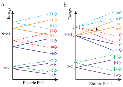
Figure 5a shows the model by Zibrov et al.Zibrov et al. (2017) and Hunt et al.Hunt et al. (2017), in this model at finite magnetic field both the orbital and spin degeneracy is lifted and the application of electric field lifts the valley degeneracyHunt et al. (2017); Zibrov et al. (2017). The other model is shown in Fig.5b, here the finite magnetic field only lifts the spin degeneracy and the electric field is responsible for lifting the valley and orbital degeneracy Lee et al. (2014); Kou et al. (2014); Maher et al. (2014); LeRoy and Yankowitz (2014).
| -1 | -2 | -3 | -4 | -5 | |
|---|---|---|---|---|---|
| -1 | (1; 1) | (0.67; 0.8) | (0.67; 0.8) | (0.67; 0.8) | (0.60; 0.8) |
| -2 | (1; 1) | (2; 2) | (2; 2) | (2; 2) | (1.5; 2) |
| -3 | (1; 1) | (2; 2) | (3; 3) | (2.67; 2.92) | (2.17; 2.93) |
| -4 | (1; 1) | (2; 2) | (3; 3) | (4; 4) | (3.5; 4) |
We find that our data can be explained by model presented in Fig. 5a [ Fig. 5b] if the (electric field) lies below [above] the LL crossing value marked by “b” in Fig. 5a [Fig. 5b]. In that scenario the different spin configuration associated with each LL edge sates is shown in the bottom row of Fig.4. The red and blue color denote the up and down spin, respectively. Table II lists the conductance value obtained using partial equilibration (Eqn. 4) and the experimental data. Each round bracket in Table II, from left to right lists the conductance value obtained using partial equilibration (Eqn. 4) followed by experimental value. We would like to mention that our data is more suitable with Fig. 5aZibrov et al. (2017); Hunt et al. (2017) as can be seen from Fig. 3b that the values of for the unipolar edges in Table I is far below the , at which LL crossing happens (“b” marker in Fig. 5a).
We find that although partial equilibration modelAmet et al. (2014) can explain data for from to but it fails to explain the quantized conductance value at and .
Moreover, the conductance value obtained at different for and are also not consistent with the partial equilibration model. The inconsistency between the values obtained by partial equilibration model and the experimental data is highlighted with yellow color in Table II, where one can clearly see that experimental values are always higher than the partial equilibration model suggesting lack of equilibration between the transmitting edges and the circulating edges under the top gate region.
The partial equilibration model assume the equal amount of equilibration between the transmitting edges () and the circulating edges () under the top gate region depending on their spin polarization irrespective of their spacial location (bottom panel of Fig. 4). The lack of equilibration in our experiment suggests that the equal amount of equilibration between all the edges may not be completely true and possibly the equilibration between the nearest edge states of transmitting edge () and circulating edge () in Fig. 4 is stronger compared to innermost circulating edge. For example, when the conductance value will be for and due to opposite spin configuration, however, for the equilibration between and (same spin polarization) will be very weak as they are spatially separated as well as due to the screening by the inner and edges in Fig. 4. Similarly, it can explain for Fig. 4c-4g and and Fig. 4d-4h. However, further theoretical studies are required to understand the equilibration for symmetry broken edges in bilayer graphene.
We now focus in the bipolar regime where the complete mixing of edge states is observed (Table I) eventhough the spin polarizations of the edges are opposite as can be seen in Fig. 5. However, this is not surprising as LaGasse et al.LaGasse and Lee (2016) have shown that for the nm width of p-n junction the landau levels are superimposed on each other as it is comparable to magnetic length scale and the full mixing of edge states are observed. In our top gated device geometry we estimate the width of pn junction to be nm, and thus the edges at the pn junction are not well defined. Not only that in the bipolar regime strong in-plane electric field is present across our sharp p-n junction and studies Lukose et al. (2007); Gu et al. (2011); Peres and Castro (2007) predict the collapse of LL due to the effective higher magnetic length scale. However, further studies are required to understand the exact nature of edge mixing mechanism in BLG.
VI Conclusion
In conclusion, our study provides the first experimental evidence of edge state equilibration in bilayer graphene when all the degeneracies of zeroth energy level are completely lifted. Although the partial equilibration based on spin polarization is able to explain most of the conductance values in the unipolar regime but still unable to capture for all the edge states. The lack of equilibration is better understood by considering the predominant mixing between the nearest edges. In the bipolar regime full equilibration is observed irrespective of the spin configurations and understood in terms of LL collapsing at the sharp pn junction.
References
- Kane et al. (1994) C. Kane, M. P. Fisher, and J. Polchinski, Physical review letters 72, 4129 (1994).
- Kane and Fisher (1997) C. Kane and M. P. Fisher, Physical Review B 55, 15832 (1997).
- Bid et al. (2010) A. Bid, N. Ofek, H. Inoue, M. Heiblum, C. Kane, V. Umansky, and D. Mahalu, Nature 466, 585 (2010).
- Williams et al. (2007) J. Williams, L. DiCarlo, and C. Marcus, Science 317, 638 (2007).
- Özyilmaz et al. (2007) B. Özyilmaz, P. Jarillo-Herrero, D. Efetov, D. A. Abanin, L. S. Levitov, and P. Kim, Physical review letters 99, 166804 (2007).
- Liu et al. (2008) G. Liu, J. Velasco Jr, W. Bao, and C. N. Lau, Applied Physics Letters 92, 203103 (2008).
- Lohmann et al. (2009) T. Lohmann, K. von Klitzing, and J. H. Smet, Nano letters 9, 1973 (2009).
- Velasco Jr et al. (2009) J. Velasco Jr, G. Liu, W. Bao, and C. N. Lau, New Journal of Physics 11, 095008 (2009).
- Ki and Lee (2009) D.-K. Ki and H.-J. Lee, Physical Review B 79, 195327 (2009).
- Ki et al. (2010) D.-K. Ki, S.-G. Nam, H.-J. Lee, and B. Özyilmaz, Physical Review B 81, 033301 (2010).
- Velasco Jr et al. (2010) J. Velasco Jr, G. Liu, L. Jing, P. Kratz, H. Zhang, W. Bao, M. Bockrath, C. N. Lau, et al., Physical Review B 81, 121407 (2010).
- Jing et al. (2010) L. Jing, J. Velasco Jr, P. Kratz, G. Liu, W. Bao, M. Bockrath, and C. N. Lau, Nano letters 10, 4000 (2010).
- Woszczyna et al. (2011) M. Woszczyna, M. Friedemann, T. Dziomba, T. Weimann, and F. J. Ahlers, Applied Physics Letters 99, 022112 (2011).
- Nam et al. (2011) S.-G. Nam, D.-K. Ki, J. W. Park, Y. Kim, J. S. Kim, and H.-J. Lee, Nanotechnology 22, 415203 (2011).
- Velasco et al. (2012) J. Velasco, Y. Lee, L. Jing, G. Liu, W. Bao, and C. Lau, Solid State Communications 152, 1301 (2012).
- Bhat et al. (2012) A. K. Bhat, V. Singh, S. Patil, and M. M. Deshmukh, Solid State Communications 152, 545 (2012).
- Schmidt et al. (2013) H. Schmidt, J. Rode, C. Belke, D. Smirnov, and R. Haug, Physical Review B 88, 075418 (2013).
- Klimov et al. (2015) N. N. Klimov, S. T. Le, J. Yan, P. Agnihotri, E. Comfort, J. U. Lee, D. B. Newell, and C. A. Richter, Physical Review B 92, 241301 (2015).
- Morikawa et al. (2015) S. Morikawa, S. Masubuchi, R. Moriya, K. Watanabe, T. Taniguchi, and T. Machida, Applied Physics Letters 106, 183101 (2015).
- Kumada et al. (2015) N. Kumada, F. Parmentier, H. Hibino, D. Glattli, and P. Roulleau, Nature communications 6 (2015).
- Matsuo et al. (2015) S. Matsuo, S. Takeshita, T. Tanaka, S. Nakaharai, K. Tsukagoshi, T. Moriyama, T. Ono, and K. Kobayashi, Nature communications 6 (2015).
- Kumar et al. (2017) C. Kumar, M. Kuiri, and A. Das, Solid State Communications (2017).
- Wei et al. (2017) D. S. Wei, T. van der Sar, J. D. Sanchez-Yamagishi, K. Watanabe, T. Taniguchi, P. Jarillo-Herrero, B. I. Halperin, and A. Yacoby, Science advances 3, e1700600 (2017).
- Abanin and Levitov (2007) D. Abanin and L. Levitov, Science 317, 641 (2007).
- Amet et al. (2014) F. Amet, J. Williams, K. Watanabe, T. Taniguchi, and D. Goldhaber-Gordon, Physical review letters 112, 196601 (2014).
- Lee et al. (2014) K. Lee, B. Fallahazad, J. Xue, D. C. Dillen, K. Kim, T. Taniguchi, K. Watanabe, and E. Tutuc, Science 345, 58 (2014).
- Kou et al. (2014) A. Kou, B. E. Feldman, A. J. Levin, B. I. Halperin, K. Watanabe, T. Taniguchi, and A. Yacoby, Science 345, 55 (2014).
- Maher et al. (2014) P. Maher, L. Wang, Y. Gao, C. Forsythe, T. Taniguchi, K. Watanabe, D. Abanin, Z. Papić, P. Cadden-Zimansky, J. Hone, et al., Science 345, 61 (2014).
- LeRoy and Yankowitz (2014) B. J. LeRoy and M. Yankowitz, Science 345, 31 (2014).
- Hunt et al. (2017) B. Hunt, J. Li, A. Zibrov, L. Wang, T. Taniguchi, K. Watanabe, J. Hone, C. Dean, M. Zaletel, R. Ashoori, et al., Nature communications 8, 948 (2017).
- Zibrov et al. (2017) A. Zibrov, C. Kometter, H. Zhou, E. Spanton, T. Taniguchi, K. Watanabe, M. Zaletel, and A. Young, Nature 549, 360 (2017).
- Lukose et al. (2007) V. Lukose, R. Shankar, and G. Baskaran, Physical review letters 98, 116802 (2007).
- Peres and Castro (2007) N. Peres and E. V. Castro, Journal of Physics: Condensed Matter 19, 406231 (2007).
- Gu et al. (2011) N. Gu, M. Rudner, A. Young, P. Kim, and L. Levitov, Physical review letters 106, 066601 (2011).
- LaGasse and Lee (2016) S. W. LaGasse and J. U. Lee, Physical Review B 94, 165312 (2016).
- Wang et al. (2013) L. Wang, I. Meric, P. Huang, Q. Gao, Y. Gao, H. Tran, T. Taniguchi, K. Watanabe, L. Campos, D. Muller, et al., Science 342, 614 (2013).
- Zhang et al. (2009) Y. Zhang, T.-T. Tang, C. Girit, Z. Hao, M. C. Martin, A. Zettl, M. F. Crommie, Y. R. Shen, and F. Wang, Nature 459, 820 (2009).
- McCann and Fal’ko (2006) E. McCann and V. I. Fal’ko, Physical Review Letters 96, 086805 (2006).
- Novoselov et al. (2006) K. S. Novoselov, E. McCann, S. Morozov, V. I. Fal’ko, M. Katsnelson, U. Zeitler, D. Jiang, F. Schedin, and A. Geim, Nature physics 2, 177 (2006).
- Guinea et al. (2006) F. Guinea, A. C. Neto, and N. Peres, Physical Review B 73, 245426 (2006).
See pages - of SI.pdf