shaolb@seas.harvard.edu
Spectral alignment of single-photon emitters in diamond using strain gradient
Abstract
Solid-state single-photon emitters are attractive for realization of integrated quantum systems due to their experimental convenience and scalability. Unfortunately, however, their complex mesoscopic environments cause photons from different emitters to be spectrally distinguishable. Here we demonstrate spectral alignment of two solid-state single-photon emitters by utilizing the strain gradient. Multiple germanium vacancy (GeV) color centers in diamond are created in fabricated diamond microcantilevers using focused ion beam implantation. The strain response of the electronic energy levels of the GeV is measured by inducing an electrically controlled strain in the device. Leveraging the large strain gradient, we tune two GeVs in the spot to emit at the same optical wavelength. Simultaneous resonant excitation of two spectrally aligned GeVs is demonstrated using a narrow linewidth laser. This strain gradient tuning can be used to realize spectrally identical quantum emitters for on-chip integrated quantum systems.
Stable single-photon emitters Aharonovich et al. (2016); Kimble et al. (1977) are essential components of quantum electrodynamics experiments Bhaskar et al. (2017); Pingault et al. (2017); Sipahigil et al. (2016); Riedrich-Möller et al. (2014); Scheibner et al. (2007) and optical quantum technologies Hensen et al. (2015); O’Brien et al. (2009); Kimble (2008); O’Brien (2007); Kuhn et al. (2002). Fluorescent color centers in diamond Aharonovich and Neu (2014), as well as other atom-like emitters in solids Bracher et al. (2017); Somaschi et al. (2016); Ding et al. (2016), have emerged as a promising platform due to their outstanding optical properties and compatibility with integrated photonic approaches. Among these, inversion-symmetric emitters such as the silicon vacancy (SiV) Pingault et al. (2017); Sipahigil et al. (2016); Rogers et al. (2014); Riedrich-Möller et al. (2014); Rose et al. (2018) and germanium vacancy (GeV) Iwasaki et al. (2015); Palyanov et al. (2015); Siyushev et al. (2017); Bhaskar et al. (2017) in diamond stand out owing to their desirable optical properties such as narrow linewidth and low spectral diffusion. However, the complex mesoscopic environments of diamond color centers lead to spectral inhomogeneities between different emitters Aharonovich et al. (2016), which is a problem for many applications that rely on spectrally identical emitters.
A variety of tuning mechanisms have been used to overcome the spectral differences among solid-state emitters, including temperature Englund et al. (2007); Yoshie et al. (2004); Chen et al. (2011), electromagnetic field Kim et al. (2011); Sipahigil et al. (2012); Bernien et al. (2012), and stresses/strain Trotta et al. (2016); Chen et al. (2018); Sternschulte et al. (1994); Meesala et al. (2016). Local control of spectral properties of inversion-symmetric emitters Hepp et al. (2014); Hepp (2014) is particularly challenging since they are not sensitive to applied electrical fields, to the first order. Mechanical strain in nanostructures provides efficient and local tuning for these emitters, and has recently been used to control the emission spectrum of SiV centers embedded in microfabricated electromechanical systems Sohn et al. (2018); Meesala et al. (2018). In this work, we demonstrate that strong strain gradients that exist in microcantilevers can be used to spectrally align quantum emitters, with high spatial resolution. This could be an efficient technique for overcoming inhomogeneous distribution of emitters and improving the properties of quantum networks Sipahigil et al. (2016); Hensen et al. (2015).
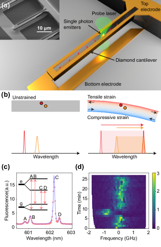
A diamond microcantilever device (Fig. 1(a)) is utilized to characterize the response of the energy levels of the GeV to applied strain and achieve a tuning of over 100 GHz in the emission spectrum. By leveraging both the large strain response of the GeV and large spatial gradient of the strain field in the device (Fig. 1(b)), we demonstrate the ability to spectrally align two GeV centers, implanted within a 50 nm spot.
The device is fabricated in a bulk diamond sample with the top surface normal to the crystal direction and the long axis of the cantilever along the direction (Fig. 1(a)). The microcantilever pattern is realized by electron-beam lithography and then transferred into the diamond via angled ion beam etching Atikian et al. (2017). The result is a suspended structure with a characteristic triangular cross sectional profile. GeV centers are introduced deterministically into the fabricated diamond cantilevers using focused ion beam implantation ( ) followed by annealing. The lateral accuracy of the implantation is better than . The resulting depth predicted by a Stopping and Range of Ions in Matter (SRIM) simulation Ziegler et al. (2010) of the implanted ions is with a straggle of . The electrodes are finally fabricated by electron-beam lithography and lift-off.
The GeV is a point defect in diamond consisting of one germanium atom positioned halfway between two adjacent missing carbon atoms. It is geometrically identical to the SiV center in diamond, and has the same symmetry. As a result, group theoretic arguments predict a qualitatively similar electronic structure for both defects Hepp et al. (2014). The excited and ground states of the GeV are separated by about in wavelength, and this transition is called the zero phonon line (ZPL). Spin-orbit coupling splits the ground (excited) state into two branches (Fig. 1(c) Inset). To resolve individual transitions, we measure the photoluminescence spectrum of GeV centers excited by a laser at temperature of which ensures that all energy levels are sufficiently populated. Four emission lines in the spectrum, marked A-D in Fig. 1(c), are identified as corresponding transitions between the excited and ground states. The C line, the transition between the lower excited state and the lower ground state, has the highest photon counts, and is the most useful for quantum optics experiments. According to a Lorentzian fit, the center wavelengths of the emission lines A-D are at , , , and , indicating a ground to excited state energy gap of , ground state splitting of , and excited state splitting of . These splittings include the effect of pre-strain in the fabricated nanostructure. The inversion symmetry of the GeV makes it robust against external electric field fluctuations to first order, resulting in a relatively stable optical transition. The measured spectra show very little frequency variation over tens of minutes despite the occasional spectral jumps (Fig. 1(d)), possibly due to strain or second order effects of electric field fluctuations in the local environment.
Finite element simulations COMSOL Inc. are used to evaluate the amount of strain induced at the location of the GeVs, in response to the applied voltage. We express the strain with respect to the local coordinates of the GeV center (Fig. 2(a) Inset). The major axis of the GeV (the line joining the two missing carbon atoms), named the Z axis, has four possible orientations along the four equivalent diamond crystal directions. The four orientations are grouped into two classes depending on the relative direction to the cantilever – transverse GeVs with their major axis lying in the transverse cross section plane (Fig. 2(b)), and longitudinal GeVs with their major axis lying in the longitudinal cross section plane (Fig. 2(c)). The two classes show qualitatively different strain responses. Fig. 2(a) shows the relation between the cantilever and local coordinate systems for the transverse GeV. For transverse GeVs, the diagonal elements of the strain tensor are shown in Fig. 2(b); the shear elements are at least one order of magnitude smaller and thus have negligible contribution to the overall strain response. Since the maximum strain in the cantilever is along the direction in the cantilever coordinate system, the strain component for transverse GeVs is small relative to the diagonal strains and . Longitudinal GeVs are rotated by with respect to transverse GeVs, so that their Y axis is aligned with the axis of the cantilever instead. Most of the strain for longitudinal GeVs is in the component.
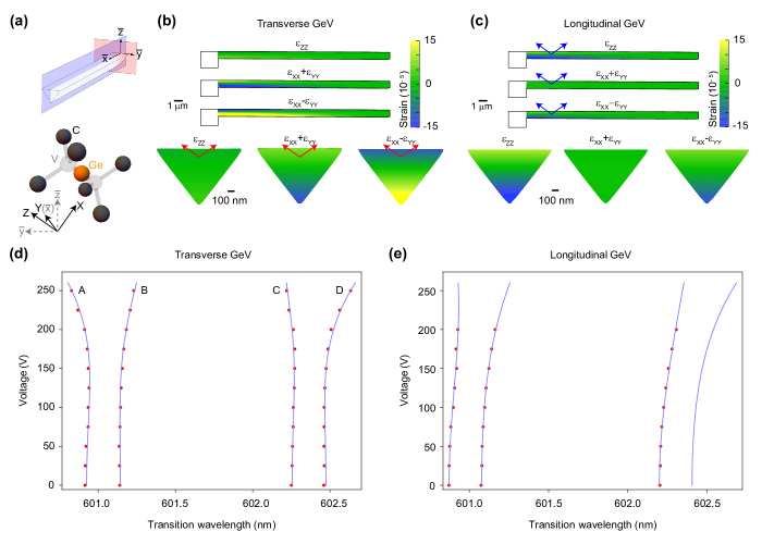
The strain terms and shift the energy levels of the GeV, while the term mixes the two orbital branches within both the ground and excited manifolds Hepp (2014). The strain tuning of the spectrum of single transverse and longitudinal GeV centers are experimentally characterized in Figs. 2(d) and (e) respectively. The spectral lines, which have a linewidth of about 1 GHz as discussed later, are tuned by several tens of linewidths. For the transverse GeV, with the maximum voltage of applied to the cantilever electrodes, the D line shows the largest shift of , while the bright C line shifts by . The maximum voltage that can be applied to the device is limited by the leakage current. For the longitudinal GeV, the C line shifts by for the maximum applied voltage of . The D line was not observed clearly for this GeV, due to low fluorescence intensity.
When the applied voltage is ramped up, the resulting increase of the splitting between A and B (equivalently, C and D) lines implies the corresponding increase in the energy splitting in the ground state manifold. Similar observations for A and C (B and D) lines indicate the increasing splitting in the excited state manifold. Fundamentally, strain affects the electronic energy levels of the GeV by deforming the orbital states. The strain interaction modifies the electronic levels of the GeV in addition to the spin-orbit and Jahn-Teller interactions Hepp et al. (2014); Hepp (2014); Meesala et al. (2018); Sohn et al. (2018). By diagonalizing the Hamiltonian of orbital states of the GeV center Sup , we obtain the electronic energy levels given by
| (1) |
where are the spin-orbit coupling strengths; and indicate ground and excited states, respectively. , , and describe the response of the GeV electronic ground or excited states to strain, which are given by
| (2) | ||||
| (3) | ||||
| (4) |
where are the components of the strain tensor given in the GeV center coordinate system shown in Figs. 2(a) and S1. , , and are the four strain susceptibility parameters describing the strain response of the GeV orbital states. The shift of the C line under strain is given by . In the limit of small strain, i.e. , the shift of the C line is . For large strains, the ground (excited) splitting terms also shift the C line significantly. The theoretical model is consistent with the experimental measurements with fitted strain susceptibilities (Figs. 2(d) and (e)).
With the spectra of both transverse and longitudinal GeVs under various strains, a fit to the above model gives spin-orbit couplings , , and an initial pre-strain of about in the term for the transverse GeV in Fig. 2(d). This is not surprising for color centers in fabricated nanostructures with thin gold layers deposited nearby. The strain susceptibility coefficients obtained from the fit are , and which are similar to that of the SiVSohn et al. (2018); Meesala et al. (2018). Further by fitting the ground and excited splitting, we estimate and . The accuracy of the estimated strain susceptibility coefficients is limited by the straggle of the implanted ion locations, as well as the large strain gradient in the device.
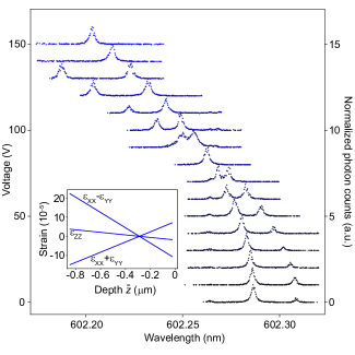
When deflected, the microcantilever has a large strain gradient in the direction (Fig. 3 Inset). As a result, two GeVs separated by tens of nanometers in depth experience a significant difference in strain, and can be tuned together spectrally with an appropriate voltage applied to the cantilever. Interestingly, there is a neutral depth in the cantilever such that GeVs above or below this depth will experience tensile or compressive strain, respectively. Hence, it is possible to tune the optical spectra of multiple GeVs in opposite directions.
We experimentally demonstrate spectral alignment of two GeVs using the strain gradient (Fig. 3), which is controlled by the voltage applied between the electrodes on the microcantilever and the substrate. To enhance the resolution of the GeV spectra, we excite the GeV transitions resonantly and count the photons emitted in the longer-wavelength phonon side band (PSB). When the probe laser is resonant with the GeV transitions, increased photon counts from the PSB are expected. Here, we have the C lines of two GeVs initially separated by . With increasing voltage, the C lines of the two GeVs get closer and overlap at a control voltage of about , crossing at higher voltages. The same shift direction of the two GeVs indicates that they are most likely in the same orientation class, i.e. transverse GeVs. From to , one GeV shifts by , while the other one shifts by . In this way, the strain gradient can bring GeVs of the same orientation class into spectral overlap, even if they are initially separated by tens of GHz.
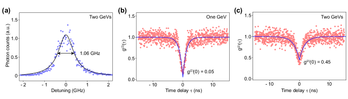
We further investigate the extent of spectral overlap of the two GeVs by measuring correlations between photons emitted into the PSB on resonant excitation of the C transitions, as shown in Fig. 4. We split the collected photons into two paths; the arrival of a photon in one path triggers a timer that stops upon detection of a photon in the other path. This measurement corresponds to the second-order autocorrelation function , where and are the intensities of PSB photon streams at time and a delayed time , respectively. When the two GeVs are spectrally distinguishable, we can only resonantly excite one GeV at a time. The fitted value of indicates a single photon source (Fig. 4(b)). Starting from the previous voltage of for spectral overlap, we finely tune the voltage between the cantilever electrodes to minimize the inhomogeneous distribution of the resonant excitation spectrum of the two GeVs (Fig. 4(a)). When the two GeVs are resonantly excited simultaneously, the fitted (Fig. 4(c)). The differs from the theoretically expected value of for two single-photon emitters, which could be a result of different excitation rates, different collection efficiencies, or different decay rates for the two GeVs.
In conclusion, the diamond nanoelectromechanical system technique is utilized to optically characterize the strain response of GeV color centers — an emerging single photon source in diamond. It provides a way to optically image the strain in diamond nanomechanical systems. Furthermore, strain gradient in an electrically deflected microcantilever is used to overcome the inhomogeneous distribution of different GeVs which renders them spectrally distinguishable. Importantly, our technique has spatial selectivity comparable to that of B-field gradient method developed for diamond NV centers Chen et al. (2013). As the strain gradient tensor provides sufficient degrees of freedom, advanced nanoelectromechanical devices with multiple electrodes could be utilized to simultaneously spectrally align multiple emitters. Furthermore, our platform may enable in situ manipulation and entanglement of multiple solid-state qubits. The ability to switch the spectral indistinguishability of quantum emitters in the same excitation volume can enable controllable local interactions and entanglement between spin qubits, and increase quantum memory density by having multiple qubits at a single spot that can be individually addressed through a single optical path. This approach can be scaled to spectrally align emitters in multiple cantilevers simultaneously, by adjusting the voltage on each cantilever appropriately.
Acknowledgements.
The authors thank Dr. Mian Zhang, Dr. Cheng Wang, Dr. Stefan Bogdanovic, Dr. Michael Burek, Dr. Vivek Venkataraman, Dr. Alp Sipahigil, Cleaven Chia, and Mihir Bhaskar for fruitful discussions, and Daniel L. Perry for the focused ion implantation. This work is supported by the Center for Integrated Quantum Materials (NSF grant No. DMR-1231319), ONR MURI on Quantum Optomechanics (Grant No. N00014-15-1-2761), NSF EFRI ACQUIRE (Grant No. 5710004174), NSF GOALI (Grant No. 1507508), and ARL CDQI (Grant No. W911NF1520067). Focused ion beam implantation was performed under the Laboratory Directed Research and Development Program at the Center for Integrated Nanotechnologies, an Office of Science User Facility operated for the U.S. Department of Energy (DOE) Office of Science. Sandia National Laboratories is a multi-mission laboratory managed and operated by National Technology and Engineering Solutions of Sandia, LLC., a wholly owned subsidiary of Honeywell International, Inc., for the U.S. Department of Energy’s National Nuclear Security Administration under contract DE-NA-0003525. S.Maity and L.S. performed experimental measurements. L.S. and Y.-I.S. fabricated the devices. S.Maity and L.S. built the experimental setups with discussions from S.Meesala. E.B. performed the focused ion beam implantation. S.Maity and L.S. prepared the manuscript with discussions from all authors. M.L. supervised this project.References
- Aharonovich et al. (2016) Igor Aharonovich, Dirk Englund, and Milos Toth, “Solid-state single-photon emitters,” Nature Photonics 10, 631–641 (2016).
- Kimble et al. (1977) H. J. Kimble, M. Dagenais, and L. Mandel, “Photon antibunching in resonance fluorescence,” Phys. Rev. Lett. 39, 691–695 (1977).
- Bhaskar et al. (2017) M. K Bhaskar, D. D Sukachev, A. Sipahigil, R. E Evans, M. J Burek, C. T Nguyen, L. J Rogers, P. Siyushev, M. H Metsch, H. Park, F. Jelezko, M. Lončar, and M. D Lukin, “Quantum nonlinear optics with a germanium-vacancy color center in a nanoscale diamond waveguide,” Physical Review Letters 118, 223603 (2017).
- Pingault et al. (2017) Benjamin Pingault, David-Dominik Jarausch, Christian Hepp, Lina Klintberg, Jonas N. Becker, Matthew Markham, Christoph Becher, and Mete Atatüre, “Coherent control of the silicon-vacancy spin in diamond,” Nature Communications 8, 15579 (2017).
- Sipahigil et al. (2016) A. Sipahigil, R. E. Evans, D. D. Sukachev, M. J. Burek, J. Borregaard, M. K. Bhaskar, C. T. Nguyen, J. L. Pacheco, H. A. Atikian, C. Meuwly, R. M. Camacho, F. Jelezko, E. Bielejec, H. Park, M. Lončar, and M. D. Lukin, “An integrated diamond nanophotonics platform for quantum-optical networks,” Science 354, 847–850 (2016).
- Riedrich-Möller et al. (2014) Janine Riedrich-Möller, Carsten Arend, Christoph Pauly, Frank Mücklich, Martin Fischer, Stefan Gsell, Matthias Schreck, and Christoph Becher, “Deterministic coupling of a single silicon-vacancy color center to a photonic crystal cavity in diamond,” Nano Letters 14, 5281–5287 (2014).
- Scheibner et al. (2007) Michael Scheibner, Thomas Schmidt, Lukas Worschech, Alfred Forchel, Gerd Bacher, Thorsten Passow, and Detlef Hommel, “Superradiance of quantum dots,” Nature Physics 3, 106–110 (2007).
- Hensen et al. (2015) B. Hensen, H. Bernien, A. E. Dréau, A. Reiserer, N. Kalb, M. S. Blok, J. Ruitenberg, R. F. L. Vermeulen, R. N. Schouten, C. Abellán, W. Amaya, V. Pruneri, M. W. Mitchell, M. Markham, D. J. Twitchen, D. Elkouss, S. Wehner, T. H. Taminiau, and R. Hanson, “Loophole-free bell inequality violation using electron spins separated by 1.3 kilometres,” Nature 526, 682–686 (2015).
- O’Brien et al. (2009) Jeremy L. O’Brien, Akira Furusawa, and Jelena Vučković, “Photonic quantum technologies,” Nature Photonics 3, 687–695 (2009).
- Kimble (2008) H. J. Kimble, “The quantum internet,” Nature 453, 1023–1030 (2008).
- O’Brien (2007) Jeremy L. O’Brien, “Optical quantum computing,” Science 318, 1567–1570 (2007).
- Kuhn et al. (2002) Axel Kuhn, Markus Hennrich, and Gerhard Rempe, “Deterministic single-photon source for distributed quantum networking,” Phys. Rev. Lett. 89, 067901 (2002).
- Aharonovich and Neu (2014) Igor Aharonovich and Elke Neu, “Diamond nanophotonics,” Advanced Optical Materials 2, 911–928 (2014).
- Bracher et al. (2017) David O. Bracher, Xingyu Zhang, and Evelyn L. Hu, “Selective purcell enhancement of two closely linked zero-phonon transitions of a silicon carbide color center,” Proceedings of the National Academy of Sciences 114, 4060–4065 (2017).
- Somaschi et al. (2016) N. Somaschi, V. Giesz, L. De Santis, J. C. Loredo, M. P. Almeida, G. Hornecker, S. L. Portalupi, T. Grange, C. Antón, J. Demory, C. Gómez, I. Sagnes, N. D. Lanzillotti-Kimura, A. Lemaítre, A. Auffeves, A. G. White, L. Lanco, and P. Senellart, “Near-optimal single-photon sources in the solid state,” Nature Photonics 10, 340 (2016).
- Ding et al. (2016) Xing Ding, Yu He, Z.-C. Duan, Niels Gregersen, M.-C. Chen, S. Unsleber, S. Maier, Christian Schneider, Martin Kamp, Sven Höfling, Chao-Yang Lu, and Jian-Wei Pan, “On-demand single photons with high extraction efficiency and near-unity indistinguishability from a resonantly driven quantum dot in a micropillar,” Phys. Rev. Lett. 116, 020401 (2016).
- Rogers et al. (2014) L. J. Rogers, K. D. Jahnke, T. Teraji, L. Marseglia, C. Muller, B. Naydenov, H. Schauffert, C. Kranz, J. Isoya, L. P. McGuinness, and F. Jelezko, “Multiple intrinsically identical single-photon emitters in the solid state,” Nat Commun 5, 4739 (2014).
- Rose et al. (2018) Brendon C. Rose, Ding Huang, Zi-Huai Zhang, Paul Stevenson, Alexei M. Tyryshkin, Sorawis Sangtawesin, Srikanth Srinivasan, Lorne Loudin, Matthew L. Markham, Andrew M. Edmonds, Daniel J. Twitchen, Stephen A. Lyon, and Nathalie P. de Leon, “Observation of an environmentally insensitive solid-state spin defect in diamond,” Science 361, 60–63 (2018).
- Iwasaki et al. (2015) T. Iwasaki, F. Ishibashi, Y. Miyamoto, Y. Doi, S. Kobayashi, T. Miyazaki, K. Tahara, K. D. Jahnke, L. J. Rogers, B. Naydenov, F. Jelezko, S. Yamasaki, S. Nagamachi, T. Inubushi, N. Mizuochi, and M. Hatano, “Germanium-vacancy single color centers in diamond,” Scientific reports 5, 12882 (2015).
- Palyanov et al. (2015) Yuri N. Palyanov, Igor N. Kupriyanov, Yuri M. Borzdov, and Nikolay V. Surovtsev, “Germanium: a new catalyst for diamond synthesis and a new optically active impurity in diamond,” Scientific Reports 5, 14789 (2015).
- Siyushev et al. (2017) Petr Siyushev, Mathias H. Metsch, Aroosa Ijaz, Jan M. Binder, Mihir K. Bhaskar, Denis D. Sukachev, Alp Sipahigil, Ruffin E. Evans, Christian T. Nguyen, Mikhail D. Lukin, Philip R. Hemmer, Yuri N. Palyanov, Igor N. Kupriyanov, Yuri M. Borzdov, Lachlan J. Rogers, and Fedor Jelezko, “Optical and microwave control of germanium-vacancy center spins in diamond,” Physical Review B 96, 081201(R) (2017).
- Englund et al. (2007) D. Englund, A. Faraon, I. Fushman, N. Stoltz, P. Petroff, and J. Vučković, “Controlling cavity reflectivity with a single quantum dot,” Nature 450, 857–61 (2007).
- Yoshie et al. (2004) T. Yoshie, A. Scherer, J. Hendrickson, G. Khitrova, H. M. Gibbs, G. Rupper, C. Ell, O. B. Shchekin, and D. G. Deppe, “Vacuum rabi splitting with a single quantum dot in a photonic crystal nanocavity,” Nature 432, 200 (2004).
- Chen et al. (2011) X.-D. Chen, C.-H. Dong, F.-W. Sun, C.-L. Zou, J.-M. Cui, Z.-F. Han, and G.-C. Guo, “Temperature dependent energy level shifts of nitrogen-vacancy centers in diamond,” Applied Physics Letters 99, 161903 (2011).
- Kim et al. (2011) Hyochul Kim, Thomas C. Shen, Deepak Sridharan, Glenn S. Solomon, and Edo Waks, “Magnetic field tuning of a quantum dot strongly coupled to a photonic crystal cavity,” Applied Physics Letters 98, 091102 (2011).
- Sipahigil et al. (2012) A. Sipahigil, M. L. Goldman, E. Togan, Y. Chu, M. Markham, D. J. Twitchen, A. S. Zibrov, A. Kubanek, and M. D. Lukin, “Quantum interference of single photons from remote nitrogen-vacancy centers in diamond,” Phys Rev Lett 108, 143601 (2012).
- Bernien et al. (2012) H. Bernien, L. Childress, L. Robledo, M. Markham, D. Twitchen, and R. Hanson, “Two-photon quantum interference from separate nitrogen vacancy centers in diamond,” Phys Rev Lett 108, 043604 (2012).
- Trotta et al. (2016) Rinaldo Trotta, Javier Martín-Sánchez, Johannes S. Wildmann, Giovanni Piredda, Marcus Reindl, Christian Schimpf, Eugenio Zallo, Sandra Stroj, Johannes Edlinger, and Armando Rastelli, “Wavelength-tunable sources of entangled photons interfaced with atomic vapours,” Nature Communications 7, 10375 (2016).
- Chen et al. (2018) H. Y. Chen, E. R. MacQuarrie, and G. D. Fuchs, “Orbital state manipulation of a diamond nitrogen-vacancy center using a mechanical resonator,” Phys. Rev. Lett. 120, 167401 (2018).
- Sternschulte et al. (1994) H. Sternschulte, K. Thonke, R. Sauer, P. C. Münzinger, and P. Michler, “1.681-ev luminescence center in chemical-vapor-deposited homoepitaxial diamond films,” Physical Review B 50, 14554–14560 (1994).
- Meesala et al. (2016) Srujan Meesala, Young-Ik Sohn, Haig A Atikian, Samuel Kim, Michael J Burek, Jennifer T Choy, and Marko Lončar, “Enhanced strain coupling of nitrogen-vacancy spins to nanoscale diamond cantilevers,” Physical Review Applied 5, 034010 (2016).
- Hepp et al. (2014) Christian Hepp, Tina Müller, Victor Waselowski, Jonas N Becker, Benjamin Pingault, Hadwig Sternschulte, Doris Steinmüller-Nethl, Adam Gali, Jeronimo R Maze, and Mete Atatüre, “Electronic structure of the silicon vacancy color center in diamond,” Physical Review Letters 112, 036405 (2014).
- Hepp (2014) Christian Hepp, Electronic structure of the silicon vacancy color center in diamond, Doctoral thesis, Naturwissenschaftlich-Technischen Fakultät II (2014).
- Sohn et al. (2018) Young-Ik Sohn, Srujan Meesala, Benjamin Pingault, Haig A. Atikian, Jeffrey Holzgrafe, Mustafa Gündŏgan, Camille Stavrakas, Megan J. Stanley, Alp Sipahigil, Joonhee Choi, Mian Zhang, Jose L. Pacheco, John Abraham, Edward Bielejec, Mikhail D. Lukin, Mete Atatüre, and Marko Lončar, “Controlling the coherence of a diamond spin qubit through its strain environment,” Nature Communications 9, 2012 (2018).
- Meesala et al. (2018) Srujan Meesala, Young-Ik Sohn, Benjamin Pingault, Linbo Shao, Haig A. Atikian, Jeffrey Holzgrafe, Mustafa Gündoğan, Camille Stavrakas, Alp Sipahigil, Cleaven Chia, Ruffin Evans, Michael J. Burek, Mian Zhang, Lue Wu, Jose L. Pacheco, John Abraham, Edward Bielejec, Mikhail D. Lukin, Mete Atatüre, and Marko Lončar, “Strain engineering of the silicon-vacancy center in diamond,” Phys. Rev. B 97, 205444 (2018).
- Atikian et al. (2017) Haig A. Atikian, Pawel Latawiec, Michael J. Burek, Young-Ik Sohn, Srujan Meesala, Normand Gravel, Ammar B. Kouki, and Marko Lončar, “Freestanding nanostructures via reactive ion beam angled etching,” APL Photonics 2, 051301 (2017).
- Ziegler et al. (2010) James F. Ziegler, M. D. Ziegler, and J. P. Biersack, “Srim – the stopping and range of ions in matter (2010),” Nuclear Instruments and Methods in Physics Research Section B: Beam Interactions with Materials and Atoms 268, 1818–1823 (2010).
- (38) COMSOL Inc., “Comsol multiphysics 5.3,” .
- (39) See Supplemental Material at [URL will be inserted by publisher] for additional details and results.
- Chen et al. (2013) Edward H. Chen, Ophir Gaathon, Matthew E. Trusheim, and Dirk Englund, “Wide-field multispectral super-resolution imaging using spin-dependent fluorescence in nanodiamonds,” Nano Letters 13, 2073–2077 (2013).