Spin transport in a graphene normal-superconductor junction in the quantum Hall regime
Abstract
The quantum Hall regime of graphene has many unusual properties. In particular, the presence of a Zeeman field opens up a region of energy within the zeroth Landau level, where the spin-up and spin-down states localized at a single edge propagate in opposite directions. We show that when these edge states are coupled to an s-wave superconductor, the transport of charge carriers is spin-filtered. This spin-filtering effect can be traced back to the interplay of specular Andreev reflections and Andreev retro-reflections in the presence of a Zeeman field.
pacs:
81.05.ue, 73.43.-f, 73.20.At, 74.45.+cI Introduction
Monolayer graphene has remarkable electronic transport properties. One of them is a peculiar quantum Hall effect, which can be observed even at room temperature novoselov07room . Inducing superconductivity via the proximity effect further enriches these transport properties heersche07bipolar ; jeong11observation ; lee15ultimately . Recently, a number of experiments have performed conductance measurements in the quantum Hall regime in monolayer graphene, using superconducting electrodes rickhaus12quantum ; park17propagation ; lee17inducing . Moreover, coupling the helical edge states within the zeroth Landau level in graphene to an s-wave superconductor can also give rise to Majorana bound states san-jose15majorana ; finocchiaro18topological .
Low-energy excitations in graphene reside in two disconnected regions in the first Brillouin zone, known as valleys. In the quantum Hall regime, the energy spectrum has an unconventional Landau level (LL) structure, where the LL energies are proportional to with integer . This discrete set of flat LLs develop into dispersive edge states toward the edge of a sample. In the low-energy approximation, the bulk LL energies in graphene are given by
| (1) |
where the valley index denotes the valley, and labels the conduction and valence band, respectively. The cyclotron frequency is given by , where is the Fermi velocity, is the magnetic length and is the absolute value of the applied magnetic field; is a nonnegative integer. These bulk LLs are fourfold degenerate: twofold for the spin and twofold for the valley degree of freedom. The valley degeneracy is lifted at the edge of the sample, where the boundary condition for the wavefunction couples the valleys peres06electronic ; brey06edge ; abanin06spin ; akhmerov07detection ; tworzydlo07valley . Hence the zeroth Landau level (ZLL) splits into two spin-degenerate bands, one with positive and one with negative energies, see Figs. 1(a) and (b).
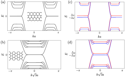
If the spin degeneracy is lifted by, e.g., a Zeeman field, each of the LLs splits into two with energy difference , where . Here, is the effective -factor of an electron in graphene and is the Bohr magneton. The energy difference between the spin-up and spin-down bulk LLs is at for the interaction-enhanced -factor, , see Refs. abanin06spin, ; volkov12interaction, . Close to the edge, the spin splitting leads to spin-up and spin-down edge states propagating in opposite directions in the energy region , see Figs. 1(c) and 1(d). Such a system can be used as a spin filter. In Ref. abanin06spin, , the authors propose a four-terminal device where the spin-filtering effect can be achieved by inducing backscattering between the counterpropagating edge states locally (using gates) in just one part of the system. The spin-filtering effect takes place due to the presence of an in-plane magnetic field and spin-orbit coupling.
Here, we suggest a different mechanism for the spin-filtering effect. We couple the edge states to an s-wave superconductor with a critical field high enough such that superconductivity and the quantum Hall effect coexist, and consider only subgap transport. The Andreev-reflected hole can have the same or the opposite direction of propagation as the electron impinging on the interface with the superconductor at energy . Which case is realized depends on the nature of the Andreev reflection in graphene that can be a retro-reflection for or a specular reflection for , see Ref. beenakker06specular, . Hence, if an incoming spin-down electron is specularly reflected while the spin-up electron is retro-reflected, spin-filtering takes place. We demonstrate this effect in the three-terminal device shown in Fig. 2. This is done by employing a tight-binding model on a honeycomb lattice within the Bogoliubov-De Gennes framework and taking into account the orbital and spin effect of the magnetic field. Note that the present work is related to but different from the idea in Ref. greenbaum07pure, . There, the charge component of a spin-polarized current is filtered away by using specular Andreev processes in the absence of an external magnetic field. However, the authors need a ferromagnetic lead to initially generate the spin-polarized current.
The rest of this article is organized as follows. In Sec. II we describe the setup of a three-terminal device and introduce its Hamiltonian. The transport coefficients of this structure are introduced and determined in Sec. III. We discuss and summarize our results in Sec. IV and conclude in Sec. V.
II Model
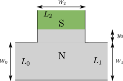
We investigate spin transport in the three-terminal device shown in Fig. 2. The underlying honeycomb lattice with lattice constant is exposed to a quantizing out-of-plane magnetic field. The upper edge of the system is coupled to an s-wave superconductor (S) with a sizable critical field, such that the quantum Hall effect and superconductivity coexist rickhaus12quantum ; park17propagation ; lee17inducing . There are two normal leads and of widths and , respectively, which serve to probe the spin-resolved transmission through the scattering region. In the rest of the paper, . The superconducting lead effectively creates a normal-superconducting interface of length that converts electrons to holes. The geometry of the system is motivated by a recent experiment park17propagation .
The tight-binding Hamiltonian of the system can be written as
| (2) |
where
| (3) | ||||
The four-spinor field is in the standard Nambu basis , where creates a particle localized at site with a four-component wavefunction . Here, the index denotes an electron (hole) with spin . The two sets of Pauli matrices, and with , describe the electron-hole and spin degree of freedom, respectively. Finally, and denote sums over all sites and over nearest neighbors.
The first (second) term in describes the nearest-neighbor hopping of electrons (holes) in an out-of-plane magnetic field with a hopping amplitude (). The Peierls phase is given by
| (4) |
where is the magnetic flux quantum and are the real-space coordinates of site . The vector potential in the Landau gauge is chosen to be constant along the -axis, . The third term in represents the Fermi energy of the system. In undoped graphene, .
The s-wave superconducting pairing is represented by and couples an electron with spin to a hole with spin on the same lattice site. The Zeeman field described by splits each energy level into two with energy difference . For simplicity, we assume the spatial dependence of the pair potential and of the magnetic field to be a step function. That is, () is assumed to be a non-zero constant (zero) in the graphene sheet below the superconducting electrode and zero (a non-zero constant) otherwise. The magnitude of the Zeeman term has the same spatial dependence as the magnetic field.
In the following, we will calculate the scattering matrix for the system shown in Fig. 2. All the numerical results for the conductances and spin polarizations presented below were obtained using Kwant groth14kwant .
III Transport coefficients
In Figs. 3(a)–3(c) we plot the relevant transport coefficients in the case when and the gap between the ZLL and other LLs is large enough so that only the ZLL plays a role. Since the Hamiltonian in Eq. (2) conserves the -projection of the spin, , only the spin-diagonal transport coefficients are shown. The transmission coefficient for a particle with spin up scattered to a particle with spin up is shown in red, while blue is used for spin-down particles. () is the probability for an electron from to be scattered into an electron (a hole) in and is the probability for an electron from to be backscattered as a hole to . Because we are in the quantum Hall regime and our system is wide enough, the probability for an electron from to be backscattered as an electron is zero () and hence not shown. It can be seen that for energies , the scattering matrix is unitary and for each spin projection.
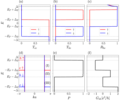
It is interesting to look at the spin polarization of the carriers in the subgap regime, where . Since conserves the spin projection along the -axis, we define the spin polarization as
| (5) |
where is the transmission coefficient for a particle with spin in lead to a particle with spin in lead . To avoid numerical artifacts, we set if the denominator in Eq. (5) is smaller than , i.e., if almost no particle is transmitted from to .
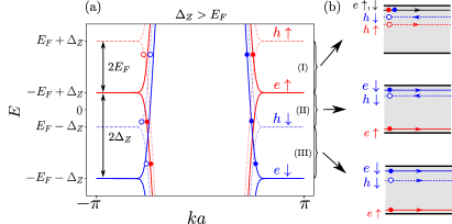
The numerically calculated spin polarization is non-zero in the energy region and zero otherwise, see Fig. 3(e). This can be understood by looking at the bandstructure and the propagation direction of the particles along the edges of the sample as illustrated in Figs. 4(a) and 4(b), respectively. In the energy region II, a spin-up electron travels undisturbed along the lower edge into , however a spin-down electron propagating along the upper edge is backscattered to as a spin-down hole because a superconductor is coupled to the upper edge. This results in the accumulation of spin-up particles in . The situation in the energy region I is the same for spin-down electrons . However, here a spin-up electron also travels along the upper edge and encounters the superconductor. Since an Andreev-reflected spin-up hole has the same propagation direction as a spin-up electron , the particle propagates along the graphene-superconductor interface via Andreev edge states, and, depending on the geometry, ends up with a certain probability as a spin-up electron or spin-up hole in . Thus, injecting spin-unpolarized particles in results in spin-polarized particles in in the energy region .
We would now like to discuss the (differential) charge conductance. Here and in the following, we assume the temperature to be . Therefore, the energy is experimentally given by the bias voltage, , where is the potential difference between the leads and . In the presence of hole excitations, the charge conductance from to is defined as
| (6) |
which is shown for our system in Fig. 3(f). In the energy region (I) the carrier ending in is a hole and , while in the region II it is an electron and . In the energy region III there is a spin-up electron along the lower edge and a spin-up hole along the upper edge propagating into , which results in zero charge transfer and . The charge conductance behavior, however, is not universal and depends on the valley structure of the edge states akhmerov07detection .
IV Discussion
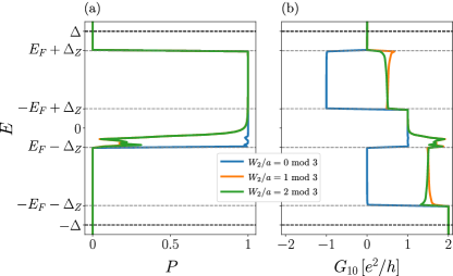
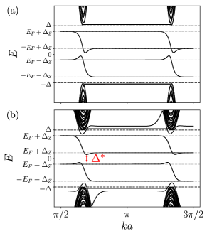
In Fig. 5 we show the spin polarization and conductance for three different widths of lead which is assumed to have armchair edge termination. We see that the spin polarization is (almost) independent of the interface length , while the charge conductance has a threefold character, depending upon the total number of hexagons across the width of the armchair ribbon being a multiple of three, or a multiple of three plus/minus one akhmerov07detection . Besides that, a set of dips (peaks) in the spin polarization (conductance) for energies close to can be observed. This feature is due to a spin-down electron leaking from to through the interface (without being Andreev-reflected). This can be understood as follows. Without the superconductor, there are edge states propagating in opposite directions for opposite spins. When we couple the superconductor to the upper edge, the electron impinging on the interface will be reflected as a hole (in the case of non-zero Andreev reflection probability). However, this hole propagates in the direction opposite to the electron edge state (for both spin projections) in this energy region. Hence, the transport along the interface should be blocked. But if the Andreev reflection probability is less than one, the electron has a finite chance to leak along the interface onto the other side. In other words, edge states along the upper edge contacted to a superconductor develop an effective gap san-jose15majorana that is smaller than the naively expected gap (for ). The bigger the pairing , the higher the Andreev reflection probability. Thus, on increasing , approaches as shown in Fig. 6.
The spin-filtering effect for is lost once the gate voltage shifts the Fermi energy such that it exceeds , i.e., the propagation direction of the electron and hole states is the same within the subgap region.
We obtain similar results if leads and have armchair orientation and lead has zigzag orientation, see Fig. 7. The spin polarization in Fig. 7(e) is again (nearly) perfect for . This is expected since, unlike the valley structure, the spin structure of the ZLL in graphene is independent of the type of the edge termination. The conductance profile in Fig. 7(f) matches the one in Fig. 5(b) for , which is the result of the same valley structure for the states at the edges of the graphene-superconductor interface for the two cases. The dip in the spin polarization is present for the same reason as in Fig. 5.
In the absence of the superconducting proximity effect ( in the graphene sheet), the spin filtering takes place in the energy region and the hole excitations play no role. The spin-filtering effect is lost for , i.e., when the spin degeneracy is restored.
V Conclusion
We have shown that spin filtering can be achieved by coupling the edge states of the spin-split zeroth Landau level in graphene to a superconductor. The spin-filtering effect can be switched on and off by applying a (global) gate voltage that shifts the Fermi energy. Unlike the charge conductance, the spin polarization is independent of the edge termination. The device can be put in different regimes by tuning the Zeeman energy independently of the gap between the zeroth Landau level and the other Landau levels. This can be achieved by applying an in-plane magnetic field giesbers09gap ; kurganova11spin ; chiappini15lifting . The spin filtering effect discussed here does not require the presence of spin-orbit coupling and its experimental verification is within the current technological capabilities.
Acknowledgements.
This work was financially supported by the Swiss National Science Foundation (SNSF) and the NCCR Quantum Science and Technology.References
- (1) K.S. Novoselov, Z. Jiang, Y. Zhang, S.V. Morozov, H.L. Stormer, U. Zeitler, J.C. Maan, G.S. Boebinger, P. Kim, and A.K. Geim, Science 315, 1379 (2007).
- (2) H.B. Heersche, P. Jarillo-Herrero, J.B. Oostinga, L.M.K. Vandersypen, and A.F. Morpurgo, Nature 446, 56 (2007).
- (3) D. Jeong, J.-H. Choi, G.-H. Lee, S. Jo, Y.-J. Doh, and H.-J. Lee, Phys. Rev. B 83, 094503 (2011).
- (4) G.-H. Lee, S. Kim, S.-H. Jhi, and H.-J. Lee, Nat. Commun. 6, 6181 (2015).
- (5) P. Rickhaus, M. Weiss, L. Marot, and C. Schönenberger, Nano Lett. 12, 1942 (2012).
- (6) G.-H. Park, M. Kim, K. Watanabe, T. Taniguchi, and H.-J. Lee, Sci. Rep. 7, 10953 (2017).
- (7) G.-H. Lee, K.-F. Huang, D.K. Efetov, D.S. Wei, S. Hart, T. Taniguchi, K. Watanabe, A. Yacoby, and P. Kim, Nat. Phys. 13, 693 (2017).
- (8) P. San-Jose, J.L. Lado, R. Aguado, F. Guinea, and J. Fernández-Rossier, Phys. Rev. X 5, 041042 (2015).
- (9) F. Finocchiaro, F. Guinea, and P. San-Jose, Phys. Rev. Lett. 120, 116801 (2018).
- (10) N.M.R. Peres, F. Guinea, and A.H. Castro Neto, Phys. Rev. B 73, 125411 (2006).
- (11) L. Brey and H.A. Fertig, Phys. Rev. B 73, 195408 (2006).
- (12) D.A. Abanin, P.A. Lee, and L.S. Levitov, Phys. Rev. Lett. 96, 176803 (2006).
- (13) A.R. Akhmerov and C.W.J. Beenakker, Phys. Rev. Lett. 98, 157003 (2007).
- (14) J. Tworzydło, I. Snyman, A.R. Akhmerov, and C.W.J. Beenakker Phys. Rev. B 76, 035411 (2007).
- (15) A.V. Volkov, A.A. Shylau, and I.V. Zozoulenko, Phys. Rev. B 86, 155440 (2012).
- (16) C.W.J. Beenakker, Phys. Rev. Lett. 97, 067007 (2006).
- (17) D. Greenbaum, S. Das, G. Schwiete, and P. G. Silvestrov, Phys. Rev. B 75, 195437 (2007).
- (18) C.W. Groth, M. Wimmer, A.R. Akhmerov, and X. Waintal, New J. Phys. 16, 063065 (2014).
- (19) A.J.M. Giesbers, L.A. Ponomarenko, K.S. Novoselov, A.K. Geim, M.I. Katsnelson, J.C. Maan, and U. Zeitler, Phys. Rev. B 80, 201403(R) (2009).
- (20) E.V. Kurganova, H.J. van Elferen, A. McCollam, L.A. Ponomarenko, K.S. Novoselov, A. Veligura, B.J. van Wees, J.C. Maan, and U. Zeitler, Phys. Rev. B 84, 121407(R) (2011).
- (21) F. Chiappini, S. Wiedmann, K. Novoselov, A. Mishchenko, A.K. Geim, J.C. Maan, and U. Zeitler, Phys. Rev. B 92, 201412(R) (2015).