Electron and Cooper pair transport across a single magnetic molecule explored with a scanning tunneling microscope
Abstract
A scanning tunneling microscope is used to explore the evolution of electron and Cooper pair transport across single Mn-phthalocyanine molecules adsorbed on Pb(111) from tunneling to contact ranges. Normal-metal as well as superconducting tips give rise to a gradual transition of the Bardeen-Cooper-Schrieffer energy gap in the tunneling range into a zero-energy resonance close to and at contact. Supporting transport calculations show that in the normal-metal – superconductor junctions this resonance reflects the merging of in-gap Yu-Shiba-Rusinov states as well as the onset of Andreev reflection. For the superconductor – superconductor contacts the zero-energy resonance is rationalized in terms of a finite Josephson current that is carried by phase-dependent Andreev and Yu-Shiba-Rusinov levels.
I Introduction
The interplay between superconductivity and magnetism has been a longstanding topic of research. It has recently witnessed a remarkable revival owing to investigations into Majorana zero modes and topological superconductivity induced by magnetic nanostructures on surfaces of -wave superconductors. Nadj-Perge et al. (2014); Feldman et al. (2016); Ruby et al. (2015a); Li et al. (2016); Ménard et al. (2017) On general grounds, it was predicted that spin-dependent scattering of Bogoliubov quasiparticles from magnetic impurities in conventional superconductors cause Yu-Shiba-Rusinov (YSR) states Yu (1965); Shiba (1968); Rusinov (1969) that modify the density of states (DOS) of the superconductor and appear as characteristic spectroscopic features within the Bardeen-Cooper-Schrieffer (BCS) Bardeen et al. (1957) energy gap. Early experiments using planar proximity tunneling junctions of CuX (XMn, Cr, Fe) and AuFe alloys, Scholten et al. (1977) thermal conductivity Przybysz and Ginsberg (1976) and specific-heat Dumoulin et al. (1977) measurements of InMn, InCr, PbMn alloys as well as Mn-implanted Pb films Bauriedl et al. (1981) were interpreted on the basis of YSR states.
Locally, i. e., at the single-atom level, the spectroscopic signature of YSR states was first reported in experiments with a scanning tunneling microscope (STM) on single Mn and Gd adsorbed on Nb(110) surfaces. Yazdani et al. (1997) In the spectra of the differential conductance (), a pair of peaks appeared at sample voltages (: binding energy of the YSR state, e: elementary charge), reflecting the electron () and hole () component of the excitation. The peak heights of these signatures were asymmetric, which was ascribed to the lack of electron-hole symmetry of the band structure Flatté and Byers (1997a, b) or the nonmagnetic scattering potential of the impurity. Balatsky et al. (2006); Salkola et al. (1997)
Renewed interest in YSR states has recently been initiated in spectroscopy of Mn and Cr atoms on superconducting Pb films on Si(111). Ji et al. (2008, 2010) In these reports, YSR states with different angular momentum could be resolved owing to the enhanced energy resolution that was achieved by low temperatures and the use of superconducting tips. Moreover, in the seminal experimental work on the competition between Cooper pairing and Kondo screening Franke et al. (2011) it was further demonstrated that an increased exchange coupling between the magnetic impurity and the superconductor leads to a decrease of and a crossing of with the Fermi level accompanied by the inversion of the electron-hole spectral weight. Several other works followed presenting the requirement of topological Shiba bands for the observation of Majorana modes in atomic chains, Nadj-Perge et al. (2013) the impact of magnetic anisotropy on YSR states, Hatter et al. (2015) the influence of the dimensionality of the superconductor on the spatial coherence of the bound states, Ménard et al. (2015) a detailed understanding of the orbital origin of YSR multiplets, Ruby et al. (2016); Choi et al. (2017) the occurrence of YSR states in proximity-induced superconductor–molecule junctions, Island et al. (2017) the spin polarization of YSR states, Cornils et al. (2017) and coupling phenomena. Kezilebieke et al. (2017)
Studies of the effects of charge transport across superconductor – normal-metal (S–N) and superconductor – superconductor (S–S) interfaces containing a single magnetic impurity on the bound in-gap states add some degree of complexity since Andreev reflection (AR) Andreev (1964) and Josephson currents Josephson (1962) have to be considered. Recently, the tunneling process via YSR states has been scrutinized for various tunneling currents. Ruby et al. (2015b) At elevated tunneling rates single-electron and Andreev tunneling have been demonstrated to contribute to the current across the junction and to cause an inversion of the YSR peak height asymmetry. However, while spectroscopy of YSR states induced by single magnetic molecules or atoms has thoroughly been investigated in the tunneling range (vide supra), the contact range, i. e., the ballistic electron transport across the junction in the absence of the tunneling barrier, has remained unexplored so far. Here, we aim at filling this gap by following the evolution of the excitation spectrum of a superconductor with adsorbed magnetic impurities from the tunneling to the contact range. Contact to single Mn-Pc molecules adsorbed on Pb(111) is reached for junction conductances exceeding (: quantum of conductance, h: Planck constant), which is more than an order of magnitude larger than previously reported single-Mn junction conductances. Ruby et al. (2015b) Using normal-metal W and superconducting Pb tips the evolution of the BCS energy gap together with in-gap YSR states has been analyzed by spectroscopy and transport calculations for the wide range of junction conductances covering tunneling to contact. In S–N as well as S–S junctions the spectra unveil a gradual broadening of the YSR peaks with increasing junction conductance and the occurrence of a broad zero-bias resonance close to and at contact. The calculations trace the broadening of YSR line widths to the increasing tip–molecule hybridization. For W–Mn-Pc–Pb(111) junctions the zero-bias peak is induced by AR owing to the high transparency of the S–N interface in the contact geometry. In the case of Pb–Mn-Pc–Pb(111) contacts the zero-bias resonance arises due to a Josephson supercurrent that is carried by phase-dependent Andreev and YSR states.
II Experiment
The experiments were performed with an STM operated at low temperature () and in ultrahigh vacuum (). Clean and single-crystalline Pb(111) surfaces were obtained after repeated cycles of Ar+ bombardment and annealing. The cleaned surface was exposed at room temperature to a beam of Mn-Pc molecules sublimated from powder (purity: ) in a heated Ta crucible. Normal-metal tips were fabricated from chemically etched W wire (purity: ), while superconducting tips were obtained by coating W tips with Pb substrate material. The doubling of the BCS energy gap width of Pb(111) was used as an indicator for the superconducting state of the tip. Constant-height spectra of were acquired by sinusoidally modulating () the bias voltage and recording the current response of the junction with a lock-in amplifier. Modulation voltages of and were applied in the case of W and Pb-coated W tips, respectively. All STM images were recorded at constant current with the bias voltage applied to the sample.
II.1 Tunneling range
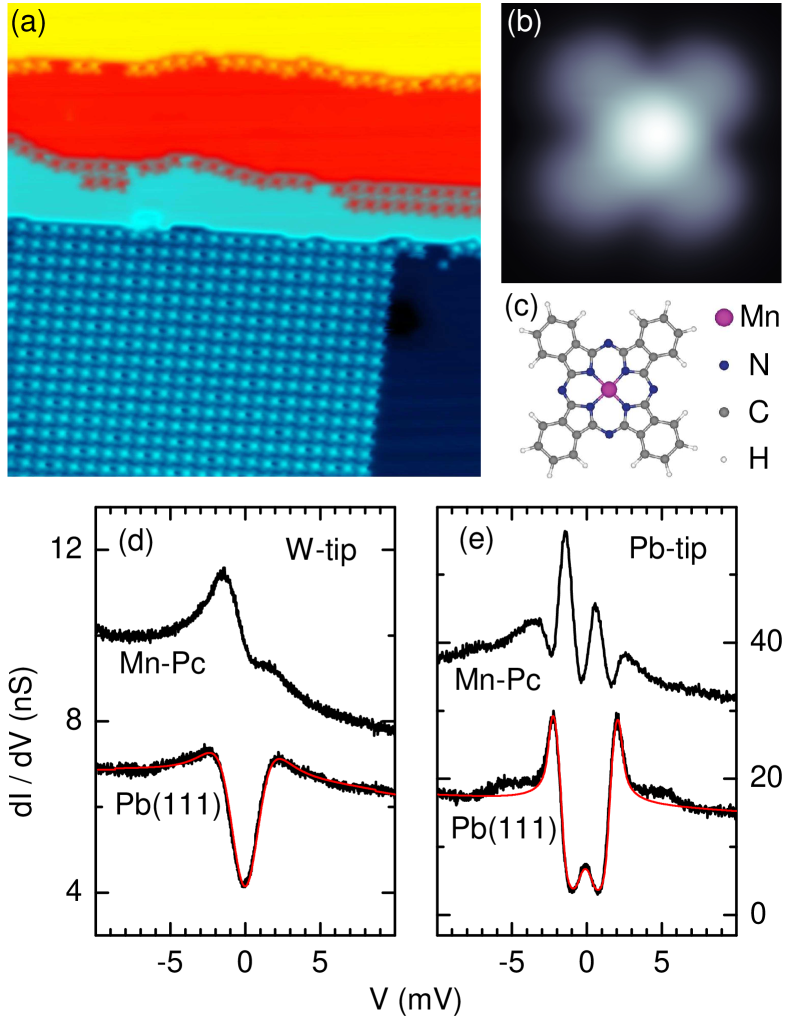
Figure 1(a) shows an STM image of Mn-Pc molecules adsorbed on Pb(111) in the submonolayer coverage range. Individual molecules appear with the characteristic crosslike shape and a bright center [Fig. 1(b)]. The four lobes are due to the phenyl groups [Fig. 1(c)] of the molecule hosting the delocalized -electron system. The Mn atom gives rise to the brightest contrast in STM images due to its -orbitals. Similar findings were reported for other metallophthalocyanines on metal surfaces. Takada and Tada (2004); Zhao et al. (2005); Kröger et al. (2007); Gopakumar et al. (2009, 2011); Liu et al. (2013); Gottfried (2015); Topyła et al. (2016) At this coverage, Mn-Pc molecules decorate step edges and form extended regular arrays on terraces [lower part of Fig. 1(a)]. Since the main focus of this article is the investigation of charge transport the structural properties are briefly summarized. For details the reader is referred to previous reports, Hao et al. (2011); Jiang et al. (2011) which are in agreement with our findings. The Mn-Pc molecules are assembled in a nearly square arrangement with a nearest-neighbor distance of and with an angle of enclosed by the lattice vectors of the molecular superstructure. One of these lattice vectors deviates by from a Pb(111) crystallographic direction. The molecular unit cell is not primitive since individual molecules adopt rotational orientations that differ by . As a consequence, the unit cell is a parallelogram containing molecules. While the molecular superstructure is incommensurate with the Pb(111) lattice Hao et al. (2011); Jiang et al. (2011) isolated Mn-Pc molecules were previously demonstrated to preferably adsorb with their Mn center at on-top sites of the substrate. Jiang et al. (2011)
In a next step, spectra were acquired atop Pb(111) and Mn-Pc molecules embedded in the array. Pristine W [Fig. 1(d)] and Pb-coated W [Fig. 1(e)] tips were used to this end. The lower spectra in Fig. 1(d), (e) show the BCS energy gap of Pb(111). The increase in energy resolution upon using a superconducting tip is obvious. The condensation peaks clearly appear at [Fig. 1(e)]. In addition, the contribution of thermally excited quasiparticles is visible as a weak zero-bias peak [Fig. 1(e)], which is not resolved in the case of a W tip [Fig. 1(d)]. Moreover, well resolved features at are discernible, which are not described by the BCS quasiparticle DOS [solid line in Fig. 1(e)]. Their origin is a van Hove singularity in the Pb(111) phonons DOS, McMillan and Rowell (1965) whose energy has to be corrected for the energy gap. Ji et al. (2008) The enhancement of the resolution is in accordance with previous reports Ji et al. (2008, 2010) and is due to the sharp onsets of condensation peaks in the tip DOS. Fits of the BCS quasiparticle DOS (solid lines) to the experimental data give rise to gap widths of the sample and of the tip. The extracted corresponds to a sample temperature of , which is close to the actual experimental temperature of . The energy gap at is with a critical temperature of . Townsend and Sutton (1962) The nearly doubled gap width in spectra acquired with a Pb-coated W tip demonstrates the superconducting state of the tip.
On top of Mn-Pc molecules, the spectra differ markedly due to the presence of intragap YSR states. Using a normal-metal W tip the energy resolution is not sufficient to observe the individual YSR states. Rather, a distorted BCS energy gap appears in the spectra [upper data set of Fig. 1(d)]. With a superconducting Pb-coated W tip, however, YSR states can individually be resolved within the gap [upper data set of Fig. 1(e)]. Depending on the Mn-Pc molecule embedded in the island the acquired spectra differ with respect to the position of the YSR-associated peaks and their height ratio. As exposed above, the molecular array is not commensurate with the Pb(111) lattice, which results in different adsorption sites for Mn-Pc molecules that entail different magnetic couplings of Cooper pairs to the screened magnetic moment of Mn-Pc. Franke et al. (2011) The asymmetric background visible in all spectra is due to a Kondo resonance, which covers a larger voltage range than the BCS energy gap. Franke et al. (2011)
II.2 Contact range
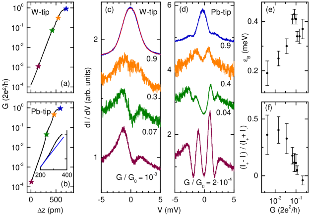
We now explore the evolution of the BCS energy gap and YSR spectroscopic signatures with increasing junction conductance. Some aspects have already been identified for high-conductance junctions in the tunneling range for single Mn atoms adsorbed on Pb(111). Ruby et al. (2015b) Here, we are particularly interested in the situation at contact and beyond; that is, the electron transport across Mn-Pc will be probed without tunneling barrier between the tip and the molecule. To this end, pristine and Pb-coated W tips were approached towards an Mn-Pc molecule and the conductance, , was simultaneously recorded. Typical traces are plotted as a function of the tip displacement, , for a W [Fig. 2(a)] and a Pb-coated W [Fig. 2(b)] tip. After exponentially increasing in the tunneling range [ (W tip), (Pb tip)] with increasing , starts to gradually level off at for W tips and at for Pb tips with contact conductances of (W tip) and (Pb tip). Akin conductance variations were reported for various molecules on diverse surfaces. Kröger et al. (2008); Berndt et al. (2010)
At the indicated conductances [stars in Fig. 2(a), (b)] spectra were acquired atop the Mn center. For pristine W tips, a representative evolution is plotted in Fig. 2(c). The asymmetric profile of the spectrum in the tunneling range consists of broad features, which are assigned to the superposition of BCS condensation peaks and YSR signatures riding on a broad Kondo resonance background. With increasing junction conductance the energy range of the BCS gap is progressively replaced by a zero-bias resonance close to and at contact.
The occurrence of a zero-bias peak for high-conductance junctions is reminiscent of AR. Agraït et al. (1992); Hauptmann et al. (2009); Brand et al. (2017) For single-C60 junctions on Nb(110) it was shown that with a normal-metal W tip the BCS gap evolved into a zero-bias peak with increasing junction conductance up to contact. Brand et al. (2017) On the basis of the Blonder-Tinkham-Klapwijk (BTK) Blonder et al. (1982) model and transport calculations this evolution was traced to the occurrence of AR at elevated tip–surface coupling. Brand et al. (2017)
In the BTK model the transparency of the S–N interface for electron transport is controlled by the Dirac function of weight , which gives rise to the normal-state transmission . By considering the BTK sample DOS at zero temperature, [: sample DOS in the nonsuperconducting state; (): energy-dependent probability for Andreev (ordinary) reflection], and taking spectroscopic broadening due to temperature and bias voltage modulation appropriately into account Brand et al. (2017) the experimental data at elevated S–N junction conductance were reproduced [solid line in Fig. 2(c)]. The suggested AR scenario is further corroborated by a previous publication reporting the electron transport across S–S single-Mn junctions. Ruby et al. (2015b) In the range of weak tip–surface coupling the electron transport in tunneling junctions was rationalized in terms of single-particle tunneling; that is, electrons or holes injected into the YSR relax to the quasiparticle continuum. With increasing injection rate this single-particle picture is no longer applicable. Rather than relaxing into the quasiparticle continuum the electron injected into the unoccupied YSR state is retroreflected as a hole into the occupied YSR state and propagates as a Cooper pair in the superconducting substrate. Ruby et al. (2015b)
The experimental spectrum at contact [topmost spectrum in Fig. 2(c)] together with the BTK fit (solid line) show that the maximum at exceeds the normal-state tails () by a factor 1.5 rather than , which would be expected for ideal AR. Blonder et al. (1982) The most likely reason for this observation is the temperature-induced broadening of the AR peak. A reduction of the ideal zero-bias AR conductance may likewise occur in the case of a spin-polarized current across the junction, which owing to the presence of a magnetic molecule may be expected. Indeed, S–N quantum point contacts were suggested and used to extract the spin polarization via the reduced AR conductance de Jong and Beenakker (1995); Soulen et al. (1998); Upadhyay et al. (1998); Ji et al. (2001); Kikuchi et al. (2001); Kant et al. (2002) on the basis of a modified BTK model. Soulen et al. (1998); Strijkers et al. (2001) In the present case, however, the spectroscopic broadening due to the finite temperature exceeds of the superconducting order parameter, which hampers the univocal assignment of the AR conductance decrease to spin polarization of the current.
Using Pb-coated W tips more spectroscopic details are available owing to the superconducting state of the tip and the concomitant increase of resolution. Figure 2(d) shows the evolution of the BCS energy gap with clearly resolved BCS condensation and YSR peaks from tunneling (bottom) to contact (top) ranges. The most obvious change is the filling of the BCS gap with a single zero-bias resonance close to and at contact. At contact [topmost data in Fig. 2(d)] the maximum of the resonance exceeds the normal-state at by . These observations are reminiscent of Cooper pair tunneling observed from symmetric Naaman et al. (2001) and asymmetric Ternes et al. (2006) STM S–S junctions. Indeed, the calculations discussed in the following section show that this zero-bias peak results from a Josephson supercurrent that is carried by phase-averaged Andreev and YSR levels. In the range of junction conductances () where the YSR features can be resolved as individual peaks their energy slightly increases [Fig. 2(e)], while the asymmetry of peak heights, [: signal strength of the YSR state in spectra at positive () and negative () bias voltage, Fig. 2(f)], is reduced with increasing conductance and even crosses close to contact. YSR energies and peak height asymmetries were extracted from fits to the experimental data where the BCS quasiparticle DOS of the tip was convoluted with the sample DOS represented by two Lorentzians for the YSR states and a symmetric gap around the Fermi energy. Franke et al. (2011) The observed increase of with tip approach may be interpreted in terms of a reduced magnetic exchange interaction of the central Mn atom and the Pb(111) Cooper pairs in the following sense. The conductance-versus-displacement data depicted in the inset to Fig. 2(b) show deviations from a simple exponential behavior in the range . Such behavior is indicative of relaxations in the junction geometry. Limot et al. (2005); Néel et al. (2007); Kröger et al. (2007); Néel et al. (2008); Kröger et al. (2009); Wang et al. (2010); Altenburg et al. (2010); Néel et al. (2011); Lazo et al. (2012); Müller et al. (2016); Calvo et al. (2018); Sabater et al. (2018) In the present case the Mn atom may be attracted towards the tip apex. Concomitantly, Mn is lifted away from the surface and effectively reduces the exchange interaction. The trading of peak height is in agreement with findings for single Mn atoms on Pb(111). Ruby et al. (2015b)
III Theory
III.1 Hamiltonian and methods
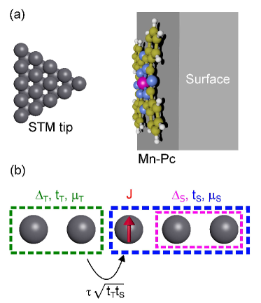
In this section, a Hamiltonian is proposed in order to capture the physics of the experimental findings, including the crossover from the tunneling to the contact range. The experimental setup is schematically sketched in Fig. 3(a). The minimal model reduces the complex setup to two semi-infinite linear atomic chains representing the tip [green dashed line in Fig. 3(b)] and the molecule-covered substrate (blue dashed line). The Hamiltonian describes the electronic states in the tip, , the superconducting substrate and the magnetic molecule, , and the coupling, , between them, i. e.,
| (1) |
The Hamiltonian describing the substrate and the molecule reads
| (2) | |||||
where () denotes the creation (annihilation) of an electron in the substrate () or at the molecule () with spin (arrows indicate the spin direction with respect to the magnetic moment of the molecule). The electrons are assumed to move in a single band with hopping , an energy offset and uniform -wave superconducting pairing vanishing at the molecule (). At the site of the molecule an exchange interaction, , is added [Fig. 3(b)].
Analogously, for the tip () a single band with hopping , energy offset and superconducting -wave order parameter is used; that is,
| (3) | |||||
The coupling between the tip and the molecule-covered substrate is mediated via the molecule at site with a hopping amplitude , where the dimensionless parameter controls the total transparency of the junction, i. e.,
| (4) |
In this way, the tunneling regime corresponds to , whereas mimics the contact range with full transparency.
Choosing () a normal-metal (superconducting) tip may be modeled. In addition, the variation of from to describes the transition from the tunneling to the contact range. In general, the effective hopping of the tip and the substrate , and their energy offsets and are expected to be different. For the sake of simplicity, however, we choose and . This assumption does not change the results qualitatively.
The previous Hamiltonian defines two semi-infinite systems [Fig. 3(b)]. In the case of the normal-metal tip is calculated by means of the -matrix formalism. The spectral function () of the tip and the surface is derived by solving the Dyson equation , where is the electron energy, a damping constant, the on-site matrix, and the hopping matrix for the specific part. These two Green functions are the basis for computing the full Green function of a subsystem involving part of the tip and part of the substrate surface as , where is the induced self-energy and the on-site Hamiltonian of the subsystem. With the full Green function and the hybridization functions the -matrix follows from the Fisher-Lee approach. Fisher and Lee (1981) Taking the -matrix as , the different transmission () and reflection () matrices can be calculated as and with the unity matrix. Focusing on an incoming electron from the normal-metal tip, the total conductance reads , Blonder et al. (1982) where is the number of channels, the electron-electron and the electron-hole reflection coefficient. and are calculated as , where is the relevant block (electron-electron or electron-hole) of the reflection matrix.
This procedure is only valid if one of the leads is a normal metal, which allows to define electron reflection and transmission coefficients. In the case of two superconducting leads the calculation of the current is more complicated and we will adopt a different strategy (vide infra) to study the spectral function and its dependence on the superconductor phase difference.
III.2 Normal-metal tip
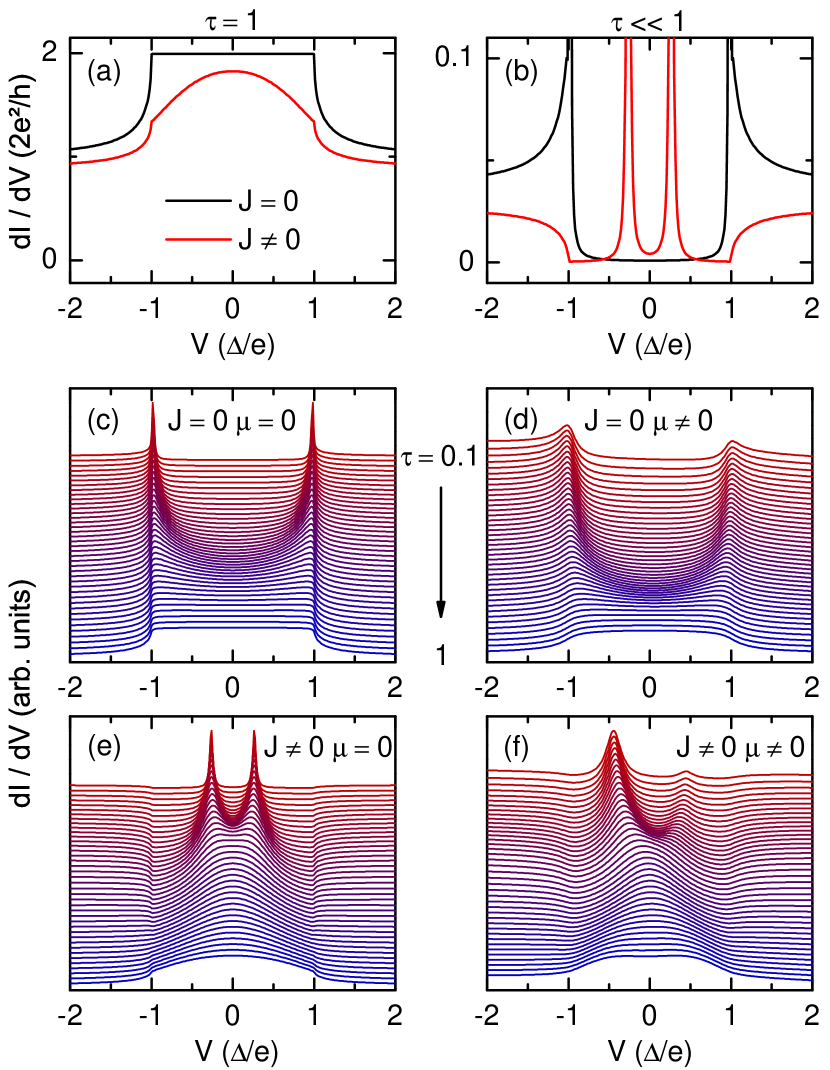
In this section the S–N junction is considered, i. e., , , in the idealized situation where and the spectral broadening vanishes. In this case can be calculated within the BTK theory using the scattering-matrix formalism. Figure 4(a) shows the calculated for the perfectly transparent () S–N interface without (top graph) and with (bottom) magnetic impurity. For the AR reflection plateau is obtained in the voltage range . At finite exchange interaction () the AR plateau transforms into a broad resonance peak due to backscattering effects. Therefore, the occurrence of the broad resonance in the experiments can be interpreted as the onset of AR.
In the tunneling range [, Fig. 4(b)] the calculated reflects the spectral function of the surface. Without magnetic impurity the spectral function consists of the BCS energy gap, whereas in the presence of the magnetic impurity () YSR states appear in the gap. In Fig. 4(c)–(f) the evolution of with increasing (top: , bottom: ) is shown. For [Fig. 4(c), (d)] our method correctly reproduces the standard evolution from the tunneling range, where is proportional to the BCS DOS of the substrate, to the AR regime. While for [Fig. 4(c)] the calculated data are symmetric with respect to zero voltage, using [Fig. 4(d)] removes the electron-hole symmetry and results in asymmetric curves. For [Fig. 4(e), (f)] the data exhibit in-gap YSR peaks for small that gradually evolve into a broad zero-voltage resonance with increasing . In particular, the case without electron-hole symmetry [Fig. 4(f)] together with some sizable broadening matches the experimental situation of Fig. 2(c) quite well. It captures the different signal strengths of the YSR peaks in the tunneling range as well as their evolution into a single peak with increasing . Therefore, the experimentally observed zero-bias peak close to and at contact reflects a superposition of the AR signature and broadened YSR levels.
III.3 Superconducting tip
The situation of a Pb tip in the experiments can be accounted for by . Due to the Josephson effect Josephson (1962) the finite bias voltage applied across the S–S junction leads to a time-dependent relative phase between the two superconductors. Anderson (1984); San-Jose et al. (2013) For the sake of simplicity, we set and with the time-dependent phase difference between the substrate and the tip. The transition between the tunneling and the contact range can qualitatively be understood by comparing the spectral function of the junction in the different transport ranges for the entire range of , i. e., . The full Green function is calculated by means of the Dyson equation , which explicitly shows the dependence on the superconducting phase difference. In the following, the spectral function represents the sum over electron and hole sectors and therefore appears symmetric for positive and negative energies, respectively. An asymmetry is present if electron and hole sectors are considered separately.
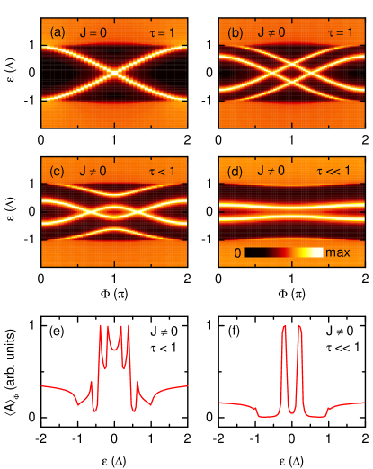
In the contact range, , and without magnetic impurity, , the spectra of of the interface show branches at positive and negative energies crossing the BCS energy gap as increases from to [Fig. 5(a)]. These branches correspond to discrete Andreev levels that carry Cooper pairs from one superconductor to the other and, thus, signal the presence of a finite Josephson supercurrent. Similar conclusions were drawn from findings obtained for microscale nanotube–superconductor junctions. Pillet et al. (2010) The slope, , is a measure of the magnitude of the Josephson current. Upon taking the magnetic impurity into account (), the original Andreev branch splits into two for positive and negative energies as shown in Fig. 5(b). These two branches become disconnected from the continuum of quasiparticle states when the transparency of the junction is reduced [Fig. 5(c)]. In the tunneling range, , the original two branches become an almost flat band signaling the presence of the conventional YSR states of the substrate [Fig. 5(d)]. The Andreev levels have essentially vanished in this transmission range.
At finite bias voltage, the phase difference evolves in time. Therefore, the phase-averaged spectral function, , was calculated [Fig. 5(e), (f)]. Close to contact, , exhibits a series of peaks around zero energy within the BCS gap [Fig. 5(e)]. Additional broadening, which may be caused by a finite temperature, would lead to a broad resonance centered around zero energy. In comparison, in the tunneling range, , only two sharp resonances appear inside the BCS gap [Fig. 5(f)]. These findings for the phase-averaged spectral function resembles the experimentally observed transition from the two in-gap peaks to a broad in-gap resonance close to and at the contact range. Before concluding, we remark that the spectral function allows to determine whether bound states exist within the superconducting energy gap and to describe their evolution with increasing junction conductance. However, the spectral function is not directly comparable with the experimental data. Indeed, the gapped energy region of the spectral function ranges from to , while the spectra exhibit the doubled BCS gap extending from to . Only more sophisticated transport calculations would improve the simulations.
IV Conclusion
Charge transport across a single magnetic molecule has been experimentally and theoretically studied for S–N and S–S STM junctions from tunneling to contact ranges. While in the tunneling range electron transport is mainly mediated by YSR states, the AR regime becomes increasingly important for larger junction conductance. In both types of junctions the conductance increase gives rise to the gradual evolution of a zero-energy resonance that reflects the broadening of YSR states due to the tip–molecule hybridization and the onset of AR. Cooper-pair transport in highly conductive S–S junctions is carried by phase-dependent Andreev and YSR levels that cause a finite Josephson supercurrent. The experimental approach of probing – characteristics of single-molecule S–N and S–S junctions from tunneling to contact ranges enables the unambiguous identification of YSR and AR states and their discrimination from other zero-bias features, such as Majorana zero modes.
Acknowledgements.
Financial support by the Deutsche Forschungsgemeinschaft through Grant No. KR 2912/10-1, the FCT (project PTDC/FIS-NAN/4662/2014 and P2020-PTDC/FIS-NAN/3668/2014), and the MINECO-Spain (MAT2016-78625-C2) is acknowledged. J. L. L. acknowledges financial support from the ETH Fellowship program.References
- Nadj-Perge et al. (2014) S. Nadj-Perge, I. K. Drozdov, J. Li, H. Chen, S. Jeon, J. Seo, A. H. MacDonald, B. A. Bernevig, and A. Yazdani, Science 346, 602 (2014), http://science.sciencemag.org/content/346/6209/602.full.pdf .
- Feldman et al. (2016) B. E. Feldman, M. T. Randeria, J. Li, S. Jeon, Y. Xie, Z. Wang, I. K. Drozdov, B. Andrei Bernevig, and A. Yazdani, Nature Physics 13, 286 (2016).
- Ruby et al. (2015a) M. Ruby, F. Pientka, Y. Peng, F. von Oppen, B. W. Heinrich, and K. J. Franke, Phys. Rev. Lett. 115, 197204 (2015a).
- Li et al. (2016) J. Li, T. Neupert, Z. Wang, A. H. MacDonald, A. Yazdani, and B. A. Bernevig, Nature Communications 7, 12297 (2016).
- Ménard et al. (2017) G. C. Ménard, S. Guissart, C. Brun, R. T. Leriche, M. Trif, F. Debontridder, D. Demaille, D. Roditchev, P. Simon, and T. Cren, Nature Communications 8, 2040 (2017).
- Yu (1965) L. Yu, Acta Physica Sinica 21, 75 (1965).
- Shiba (1968) H. Shiba, Progress of Theoretical Physics 40, 435 (1968).
- Rusinov (1969) A. I. Rusinov, Sov. Phys. JETP Letters 9, 85 (1969).
- Bardeen et al. (1957) J. Bardeen, L. N. Cooper, and J. R. Schrieffer, Phys. Rev. 108, 1175 (1957).
- Scholten et al. (1977) P. D. Scholten, J. D. Lejeune, W. M. Saslow, and D. G. Naugle, Phys. Rev. B 16, 1068 (1977).
- Przybysz and Ginsberg (1976) J. X. Przybysz and D. M. Ginsberg, Phys. Rev. B 14, 1039 (1976).
- Dumoulin et al. (1977) L. Dumoulin, E. Guyon, and P. Nedellec, Phys. Rev. B 16, 1086 (1977).
- Bauriedl et al. (1981) W. Bauriedl, P. Ziemann, and W. Buckel, Phys. Rev. Lett. 47, 1163 (1981).
- Yazdani et al. (1997) A. Yazdani, B. A. Jones, C. P. Lutz, M. F. Crommie, and D. M. Eigler, Science 275, 1767 (1997), http://science.sciencemag.org/content/275/5307/1767.full.pdf .
- Flatté and Byers (1997a) M. E. Flatté and J. M. Byers, Phys. Rev. B 56, 11213 (1997a).
- Flatté and Byers (1997b) M. E. Flatté and J. M. Byers, Phys. Rev. Lett. 78, 3761 (1997b).
- Balatsky et al. (2006) A. V. Balatsky, I. Vekhter, and J.-X. Zhu, Rev. Mod. Phys. 78, 373 (2006).
- Salkola et al. (1997) M. I. Salkola, A. V. Balatsky, and J. R. Schrieffer, Phys. Rev. B 55, 12648 (1997).
- Ji et al. (2008) S.-H. Ji, T. Zhang, Y.-S. Fu, X. Chen, X.-C. Ma, J. Li, W.-H. Duan, J.-F. Jia, and Q.-K. Xue, Phys. Rev. Lett. 100, 226801 (2008).
- Ji et al. (2010) S.-H. Ji, T. Zhang, Y.-S. Fu, X. Chen, J.-F. Jia, Q.-K. Xue, and X.-C. Ma, Applied Physics Letters 96, 073113 (2010), http://dx.doi.org/10.1063/1.3318404 .
- Franke et al. (2011) K. J. Franke, G. Schulze, and J. I. Pascual, Science 332, 940 (2011), http://science.sciencemag.org/content/332/6032/940.full.pdf .
- Nadj-Perge et al. (2013) S. Nadj-Perge, I. K. Drozdov, B. A. Bernevig, and A. Yazdani, Phys. Rev. B 88, 020407 (2013).
- Hatter et al. (2015) N. Hatter, B. W. Heinrich, M. Ruby, J. I. Pascual, and K. J. Franke, Nat. Commun. 6, 8988 (2015).
- Ménard et al. (2015) G. C. Ménard, S. Guissart, C. Brun, S. Pons, V. S. Stolyarov, F. Debontridder, M. V. Leclerc, E. Janod, L. Cario, D. Roditchev, P. Simon, and T. Cren, Nature Physics 11, 1013 (2015).
- Ruby et al. (2016) M. Ruby, Y. Peng, F. von Oppen, B. W. Heinrich, and K. J. Franke, Phys. Rev. Lett. 117, 186801 (2016).
- Choi et al. (2017) D.-J. Choi, C. Rubio-Verdú, J. de Bruijckere, M. M. Ugeda, N. Lorente, and J. I. Pascual, Nat. Commun. 8, 15175 (2017).
- Island et al. (2017) J. O. Island, R. Gaudenzi, J. de Bruijckere, E. Burzurí, C. Franco, M. Mas-Torrent, C. Rovira, J. Veciana, T. M. Klapwijk, R. Aguado, and H. S. J. van der Zant, Phys. Rev. Lett. 118, 117001 (2017).
- Cornils et al. (2017) L. Cornils, A. Kamlapure, L. Zhou, S. Pradhan, A. A. Khajetoorians, J. Fransson, J. Wiebe, and R. Wiesendanger, Phys. Rev. Lett. 119, 197002 (2017).
- Kezilebieke et al. (2017) S. Kezilebieke, M. Dvorak, T. Ojanen, and P. Liljeroth, arXiv:1701.03288v2[cond-mat.mes-hall]30Nov2017 (2017).
- Andreev (1964) A. F. Andreev, Sov. Phys. JETP 19, 1228 (1964).
- Josephson (1962) B. Josephson, Physics Letters 1, 251 (1962).
- Ruby et al. (2015b) M. Ruby, F. Pientka, Y. Peng, F. von Oppen, B. W. Heinrich, and K. J. Franke, Phys. Rev. Lett. 115, 087001 (2015b).
- Takada and Tada (2004) M. Takada and H. Tada, Chemical Physics Letters 392, 265 (2004).
- Zhao et al. (2005) A. Zhao, Q. Li, L. Chen, H. Xiang, W. Wang, S. Pan, B. Wang, X. Xiao, J. Yang, J. G. Hou, and Q. Zhu, Science 309, 1542 (2005).
- Kröger et al. (2007) J. Kröger, H. Jensen, N. Néel, and R. Berndt, Surface Science 601, 4180 (2007), eCOSS-24.
- Gopakumar et al. (2009) T. Gopakumar, N. Néel, J. Kröger, and R. Berndt, Chemical Physics Letters 484, 59 (2009).
- Gopakumar et al. (2011) T. G. Gopakumar, T. Brumme, J. Kröger, C. Toher, G. Cuniberti, and R. Berndt, The Journal of Physical Chemistry C 115, 12173 (2011), https://doi.org/10.1021/jp2038619 .
- Liu et al. (2013) L. Liu, K. Yang, Y. Jiang, B. Song, W. Xiao, L. Li, H. Zhou, Y. Wang, S. Du, M. Ouyang, W. A. Hofer, A. H. Castro Neto, and H.-J. Gao, Scientific Reports 3, 1210 (2013).
- Gottfried (2015) J. M. Gottfried, Surface Science Reports 70, 259 (2015).
- Topyła et al. (2016) M. Topyła, N. Néel, and J. Kröger, Langmuir 32, 6843 (2016), pMID: 27322189, https://doi.org/10.1021/acs.langmuir.6b01529 .
- Hao et al. (2011) D. Hao, C. Song, Y. Ning, Y. Wang, L. Wang, X.-C. Ma, X. Chen, and Q.-K. Xue, The Journal of Chemical Physics 134, 154703 (2011), http://dx.doi.org/10.1063/1.3579493 .
- Jiang et al. (2011) Y. H. Jiang, W. D. Xiao, L. W. Liu, L. Z. Zhang, J. C. Lian, K. Yang, S. X. Du, and H.-J. Gao, The Journal of Physical Chemistry C 115, 21750 (2011), http://dx.doi.org/10.1021/jp203462f .
- McMillan and Rowell (1965) W. L. McMillan and J. M. Rowell, Phys. Rev. Lett. 14, 108 (1965).
- Townsend and Sutton (1962) P. Townsend and J. Sutton, Phys. Rev. 128, 591 (1962).
- Kröger et al. (2008) J. Kröger, N. Néel, and L. Limot, J. Phys.: Condens. Matter 20, 223001 (2008).
- Berndt et al. (2010) R. Berndt, J. Kröger, N. Néel, and G. Schull, Phys. Chem. Chem. Phys. 12, 1022 (2010).
- Agraït et al. (1992) N. Agraït, J. G. Rodrigo, and S. Vieira, Phys. Rev. B 46, 5814 (1992).
- Hauptmann et al. (2009) N. Hauptmann, M. Becker, J. Kröger, and R. Berndt, Phys. Rev. B 79, 144522 (2009).
- Brand et al. (2017) J. Brand, P. Ribeiro, N. Néel, S. Kirchner, and J. Kröger, Phys. Rev. Lett. 118, 107001 (2017).
- Blonder et al. (1982) G. E. Blonder, M. Tinkham, and T. M. Klapwijk, Phys. Rev. B 25, 4515 (1982).
- de Jong and Beenakker (1995) M. J. M. de Jong and C. W. J. Beenakker, Phys. Rev. Lett. 74, 1657 (1995).
- Soulen et al. (1998) R. J. Soulen, J. M. Byers, M. S. Osofsky, B. Nadgorny, T. Ambrose, S. F. Cheng, P. R. Broussard, C. T. Tanaka, J. Nowak, J. S. Moodera, A. Barry, and J. M. D. Coey, Science 282, 85 (1998), http://science.sciencemag.org/content/282/5386/85.full.pdf .
- Upadhyay et al. (1998) S. K. Upadhyay, A. Palanisami, R. N. Louie, and R. A. Buhrman, Phys. Rev. Lett. 81, 3247 (1998).
- Ji et al. (2001) Y. Ji, G. J. Strijkers, F. Y. Yang, C. L. Chien, J. M. Byers, A. Anguelouch, G. Xiao, and A. Gupta, Phys. Rev. Lett. 86, 5585 (2001).
- Kikuchi et al. (2001) K. Kikuchi, H. Imamura, S. Takahashi, and S. Maekawa, Phys. Rev. B 65, 020508 (2001).
- Kant et al. (2002) C. H. Kant, O. Kurnosikov, A. T. Filip, P. LeClair, H. J. M. Swagten, and W. J. M. de Jonge, Phys. Rev. B 66, 212403 (2002).
- Strijkers et al. (2001) G. J. Strijkers, Y. Ji, F. Y. Yang, C. L. Chien, and J. M. Byers, Phys. Rev. B 63, 104510 (2001).
- Naaman et al. (2001) O. Naaman, W. Teizer, and R. C. Dynes, Phys. Rev. Lett. 87, 097004 (2001).
- Ternes et al. (2006) M. Ternes, W.-D. Schneider, J.-C. Cuevas, C. P. Lutz, C. F. Hirjibehedin, and A. J. Heinrich, Phys. Rev. B 74, 132501 (2006).
- Limot et al. (2005) L. Limot, J. Kröger, R. Berndt, A. Garcia-Lekue, and W. A. Hofer, Phys. Rev. Lett. 94, 126102 (2005).
- Néel et al. (2007) N. Néel, J. Kröger, L. Limot, T. Frederiksen, M. Brandbyge, and R. Berndt, Phys. Rev. Lett. 98, 065502 (2007).
- Kröger et al. (2007) J. Kröger, H. Jensen, and R. Berndt, New Journal of Physics 9, 153 (2007).
- Néel et al. (2008) N. Néel, J. Kröger, L. Limot, and R. Berndt, Nano Lett. 8, 1291 (2008), pMID: 18386913, http://dx.doi.org/10.1021/nl073074i .
- Kröger et al. (2009) J. Kröger, N. Néel, A. Sperl, Y. F. Wang, and R. Berndt, New Journal of Physics 11, 125006 (2009).
- Wang et al. (2010) Y. F. Wang, J. Kröger, R. Berndt, H. Vázquez, M. Brandbyge, and M. Paulsson, Phys. Rev. Lett. 104, 176802 (2010).
- Altenburg et al. (2010) S. J. Altenburg, J. Kröger, B. Wang, M.-L. Bocquet, N. Lorente, and R. Berndt, Phys. Rev. Lett. 105, 236101 (2010).
- Néel et al. (2011) N. Néel, J. Kröger, and R. Berndt, Nano Letters 11, 3593 (2011), pMID: 21854026, http://dx.doi.org/10.1021/nl201327c .
- Lazo et al. (2012) C. Lazo, N. Néel, J. Kröger, R. Berndt, and S. Heinze, Phys. Rev. B 86, 180406 (2012).
- Müller et al. (2016) M. Müller, C. Salgado, N. Néel, J. J. Palacios, and J. Kröger, Phys. Rev. B 93, 235402 (2016).
- Calvo et al. (2018) M. R. Calvo, C. Sabater, W. Dednam, E. B. Lombardi, M. J. Caturla, and C. Untiedt, Phys. Rev. Lett. 120, 076802 (2018).
- Sabater et al. (2018) C. Sabater, W. Dednam, M. R. Calvo, M. A. Fernández, C. Untiedt, and M. J. Caturla, Phys. Rev. B 97, 075418 (2018).
- Fisher and Lee (1981) D. S. Fisher and P. A. Lee, Phys. Rev. B 23, 6851 (1981).
- Anderson (1984) P. W. Anderson, Basic notions of condensed matter physics (Benjamin-Cummings, 1984).
- San-Jose et al. (2013) P. San-Jose, J. Cayao, E. Prada, and R. Aguado, New Journal of Physics 15, 075019 (2013).
- Pillet et al. (2010) J.-D. Pillet, C. H. L. Quay, P. Morfin, C. Bena, A. L. Yeyati, and P. Joyez, Nature Physics 6, 965 (2010).