Excitons in hexagonal boron nitride single-layer: a new platform for polaritonics in the ultraviolet
Abstract
The electronic and optical properties of 2D hexagonal boron nitride are studied using first principle calculations. GW and BSE methods are employed in order to predict with better accuracy the excited and excitonic properties of this material. We determine the values of the band gap, optical gap, excitonic binding energies and analyse the excitonic wave functions. We also calculate the exciton energies following an equation of motion formalism and the Elliot formula, and find a very good agreement with the +BSE method. The optical properties are studied for both the TM and TE modes, showing that 2D hBN is a good candidate to polaritonics in the UV range. In particular it is shown that a single layer of h-BN can act as an almost perfect mirror for ultraviolet electromagnetic radiation.
I Introduction
Two dimensional hexagonal boron nitride (hBN), also called by some white graphene, is an electrical insulator in which the boron (B) and nitrogen (N) atoms are arranged in a honeycomb lattice and are bounded by strong covalent bonds. Like graphene, hBN has good mechanical propertiesBao et al. (2016a) and high thermal conductivity.Bao et al. (2016b) Specially interesting is the possibility of using hBN as a buffer layer in van der Waals heterostructures, namelly ones comprised by layers of h-BN/graphene.Amorim et al. (2016) Hexagonal boron nitride layer can serve as a dielectric or a substrate material for graphene in order to improve its mobilityBanszerus et al. (2016) and open a gapJung et al. (1). It can also be used to improve the thermoelectric performance of graphene.Duan et al. (2016)
Yet, its electronic properties differ significantly from graphene. Graphene and electronic bands have a linear dispersion at the K point, whereas in hBN there is a lift of the degeneracy at the same point and a wide band gap greater than 7 eV is formed, at least within an independent electron picture. That would, in principle, make it ideal for optoelectronic devices in the deep ultraviolet region Li et al. (2016); Vuong et al. (2017). As we will see, however, excitonic effects play an important role in this material: excitonic peaks are created at the near UV, and this is a much more useful electromagnetic spectral range, when compared to the deep UV.
The optical properties of monolayer hBN at the UV range are characterized by the exciton with a corresponding optical band gap calculated in the range – eV (see Sec. II). The presence of the exciton in this range can be used to excite exciton-polaritons, that share some properties with surface plasmon-polaritons Basov et al. (2016); Low et al. (2017). Therefore, the UV optical properties of hBN can be used as an alternative to the emerging field of UV plasmonics. Watanabe et al. (2011); Mattiucci et al. (2012); McMahon et al. (2013); Yang et al. (2013); Maidecchi et al. (2013); Ross and Schatz (2014); Watson et al. (2015); Alcaraz de la Osa et al. (2015); Gutierrez et al. (2016); Gutiérrez et al. (2018) The plasmonics in UV range also attracts interest in biological tissue Kumamoto et al. (2011) as consequence of the resonances in nucleotide bases and aromatic amino acids. Plasmonics in this ranges relies in poor metals Knight et al. (2012); Maidecchi et al. (2013); Ross and Schatz (2014); McMahon et al. (2013) and Rhodium Watson et al. (2015); Alcaraz de la Osa et al. (2015); Gutiérrez et al. (2018).
Because of the difficulty of its synthesis, few experimental works have been done for hBN single layer. Also, to study and probe its electronic and optical properties it is necessary to work in UV range. To our best knowledge only one experimental workNagashima et al. (1995) has been produced that studies the electronic properties of 2D hBN. Those authors observed the band structure of BN monolayer on Ni(111) surface by using angle-resolved ultraviolet-photoelectron spectroscopy and angle-resolved secondary-electron-emission spectroscopy. Because the bond between the interface of h-BN and Ni(111) is weak, the band-structure observed can be regarded as that of the monolayer h-BN. The band gap was determined to be 7 eV and after a comparison with theoretical works, the authors conclude that the band gap is estimated to be within the range of 4.6 to 7.0 eV, too wide when compared with numerical results. These theoretical works were based on first principles calculations using Density Functional Theory (DFT). It is well known that DFT does not predict with good accuracy the electronic and optical properties of semiconductors and insulators. Accurate values require a theory that include many-body effects like the approximation.Hedin (1965); Hedin and Lundqvist (1970) To obtain optical properties, a theory that includes the excitonic properties is also needed. Usually, the Bethe-Salpeter equation (BSE)Salpeter and Bethe (1951); Albrecht et al. (1998) is used.
There are several works in the literature that used the approximationBlase et al. (1995); Sahin et al. (2009); Berseneva et al. (2013) and +BSECudazzo et al. (2016); Wirtz et al. (2006); Galvani et al. (2016) on 2D h-BN. The results from these works vary significantly, as can be seen in Table 1. There is no agreement even on whether the gap is direct or indirect. Convergence can be an issue in and BSE calculations as can be seen in References Ferreira and Ribeiro, 2017 and Shih et al., 2010. It is likely that the works summarized in Table 1 use different criteria for convergence and that may explain the differences.
| Reference | Calculation | KK | K | O. Gap | EBE |
|---|---|---|---|---|---|
| This work | + BSE | 7.77 | 7.32 | 5.58 | 2.19 |
| Ref. Wirtz et al.,2006 | + BSE | 7.80 | - | 6.30 | 2.10 or 1.50 |
| Ref. Cudazzo et al.,2016 | + BSE | 7.36 | - | 5.30 | 2.06 |
| Ref. Galvani et al.,2016 | + BSE | 7.25 | - | - | 1.90 |
| Ref. Berseneva et al.,2013 | - | 7.40 | - | - | |
| Ref. Sahin et al.,2009 | - | 6.86 | - | - | |
| Ref. Blase et al.,1995 | - | 6.00 | - | - |
A small number of bands used in the calculationBlase et al. (1995); Sahin et al. (2009) or not using a truncation to avoid interaction with periodic imagesBerseneva et al. (2013) may also explain some differences. Sometimes there is some ambiguity between the value stated for the gap and the one that can be obtained from the absorption spectrum presented.Wirtz et al. (2006) More difficult to explain are the values obtained in Ref. Galvani et al., 2016. They differ significantly from our work and others, although they seem to have converged the calculations carefully. One explanation may be that they fixed the lattice constant at the experimental value, instead of relaxing the unit cell. The experimental lattice constant may not match the value that actually optimizes the system and can influence the values of the gaps in the electronic band-structure. An effective-energy techniqueBerger et al. (2010) was adopted in Ref. Cudazzo et al., 2016. That technique allowed the calculation of the screened Coulomb interaction to be converged with only 90 bands and 60 bands for the self-energy calculation. The use of such technique certainly will produce some differences in the final results.
In this work we clarify whether the gap in hBN is direct or indirect, as well as their values and the exciton energies. We also calculate the excitonic spectra using an equation of motion formalism and the Elliot formula, fitting it with the +BSE calculations thus obtaining a validation of the method. In Section II we describe the details of the calculations and results. In Section III we show the results of the BSE calculations. Both and BSE calculations were performed with the software package BerkeleyGW.Deslippe et al. (2012); Hybertsen and Louie (1986); Rohlfing and Louie (2000) Section IV presents the equation of motion formalism and the results for the excitonic properties of monolayer hBN. In Section V we study the properties of exciton-polaritons of hBN and we show that a monolayer of hBN can be used as a UV mirror. We finally draw the conclusions in Section VI.
II results
calculations were done on top of DFT calculations with a scalar-relativistic norm-conserving pseudopotential. The software package Quantum ESPRESSOGiannozzi et al. (2009) was used for the DFT calculations. The details of the DFT calculations are summarized in Table 2. For calculations, a truncation technique is needed due to the non-local nature of this theory.
| Exchange-correlation functional | GGA-PBE Perdew et al. (1996) |
|---|---|
| Plane-wave cut-off | 70 Ry |
| K-point sampling (Monkhorst-Pack)Monkhorst and Pack (1976) | |
| Interlayer distance | 15.8 Å |
| Lattice constant | 2.5 Å |
We found that for DFT calculations a grid of k-points is enough to reach convergence. For the calculations, a grid of -points and a cut off energy of 22.6 Ry and 1100 bands were needed for the dielectric matrix calculations. For the self-energy calculation we used a cut off energy of 22.6 Ry and 1000 bands. The results obtained for the electronic band gap are summarized in Table 3. They show that a monolayer of hBN is a wide band-gap indirect-gap material. Fig. 1 presents the electronic band structure and electronic density of states for both DFT and calculations.
| Transition | K | KK | Optical | EBE | |
|---|---|---|---|---|---|
| Energy [eV] | 7.32 | 7.77 | 9.07 | 5.58 | 2.19 |
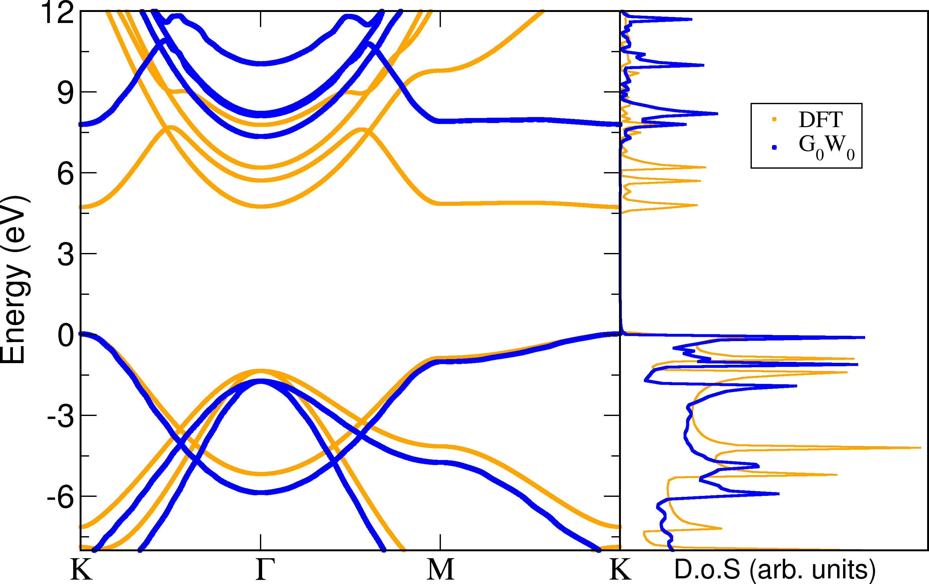
As mentioned in the Introduction, the only experimental work we are aware off is the one from Ref. Nagashima et al., 1995, which in fact estimates the band gap based on theoretical works that used mean field calculations to predict the electronic properties of bulk h-BN. Mean field theories such as DFT underestimate the band gap value of semiconductors and insulator materials. They obtain a wide range of possible values, from 4.6 to 7.0 eV. We believe that a value closer to 7.0 eV is more reliable, since the gap value for the bulk materials are lower when compared to the monolayer counterpart. And is actually closer to the ones obtained by works referred in Table 1. Still, more experimental work is needed.
Ref. Nagashima et al., 1995 also calculated the width of the valence bands, and they found no good agreement with theoretical works of the time. Table 4 shows the width of the valence bands as calculated with DFT, and the experimental determination of Ref. Nagashima et al., 1995. The -band is the one that has its highest energy at the K-point, while the and are the bands that have the highest energy at the point. Table 4 shows that DFT results differ from the experimental ones by values greater than 0.5 eV in all cases. On the other hand, results differ from the experimental results by values equal or smaller than 0.1 eV.
| Width of bands [eV] | band | band | band |
|---|---|---|---|
| This work (DFT) | 5.20 | 5.78 | 7.49 |
| This work () | 5.90 | 6.42 | 8.24 |
| ExperimentalNagashima et al. (1995) | 5.80 | 6.50 | 8.20 |
We also calculated the effective masses of the highest valence band and lowest conduction band using both and DFT (Table 5). We found no differences between and DFT, except for the effective mass at K on the first conduction band (DFT value greater by ). Thus we conclude that DFT calculations are reliable to obtain the values of the effective masses in this material.
| Effective mass | ||||
|---|---|---|---|---|
| Symmetry points | K | M | ||
| Valence band | 0.63 | 0.82 | 1.09 | 0.46 |
| Conduction band | 0.83 | 0.95 | 1.27 | 0.35 |
Ref. Blase et al., 1995 also calculated the effective mass at the point for the conduction band, and obtained a value of with only slight variations for different planar directions. In our work we obtained differences of between different directions in reciprocal space at the point.
III BSE results
After determining the conduction and valence band states, the electron-hole pair states are determined using the Bethe-Salpeter (BSE) equation. The imaginary part of the dielectric function is thenRohlfing and Louie (2000)
| (1) |
where is the energy for an excitonic state , is the velocity matrix element, and is the direction of the polarization of incident light with energy . is the electron charge.
If we do not consider excitonic effects, the expression becomes a transition between single particle statesRohlfing and Louie (2000)
| (2) |
which is a random phase approximation (RPA). The labels denotes valence (conduction) band states, and denotes the single particle momentum (only vertical transitions are considered).
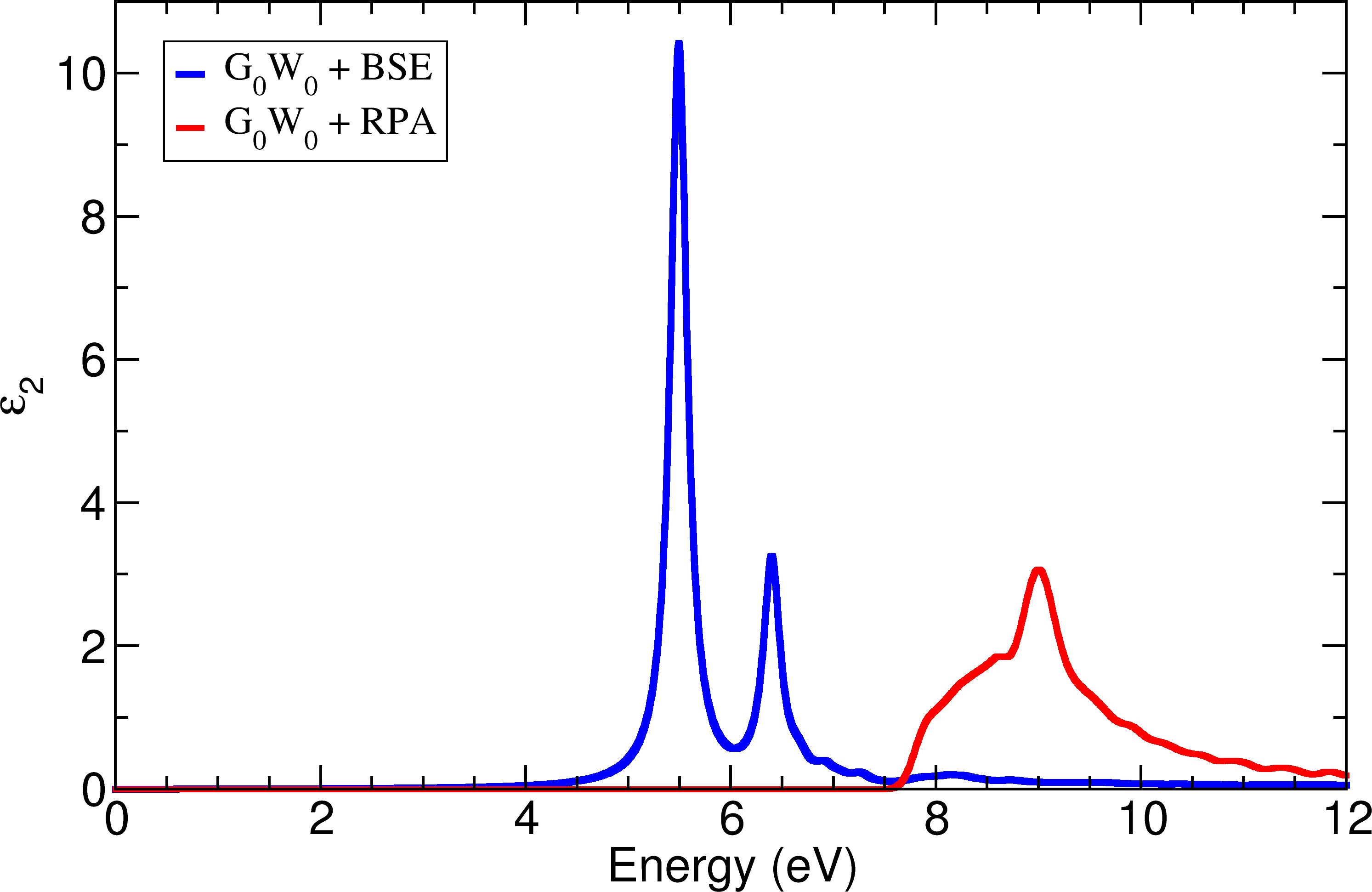
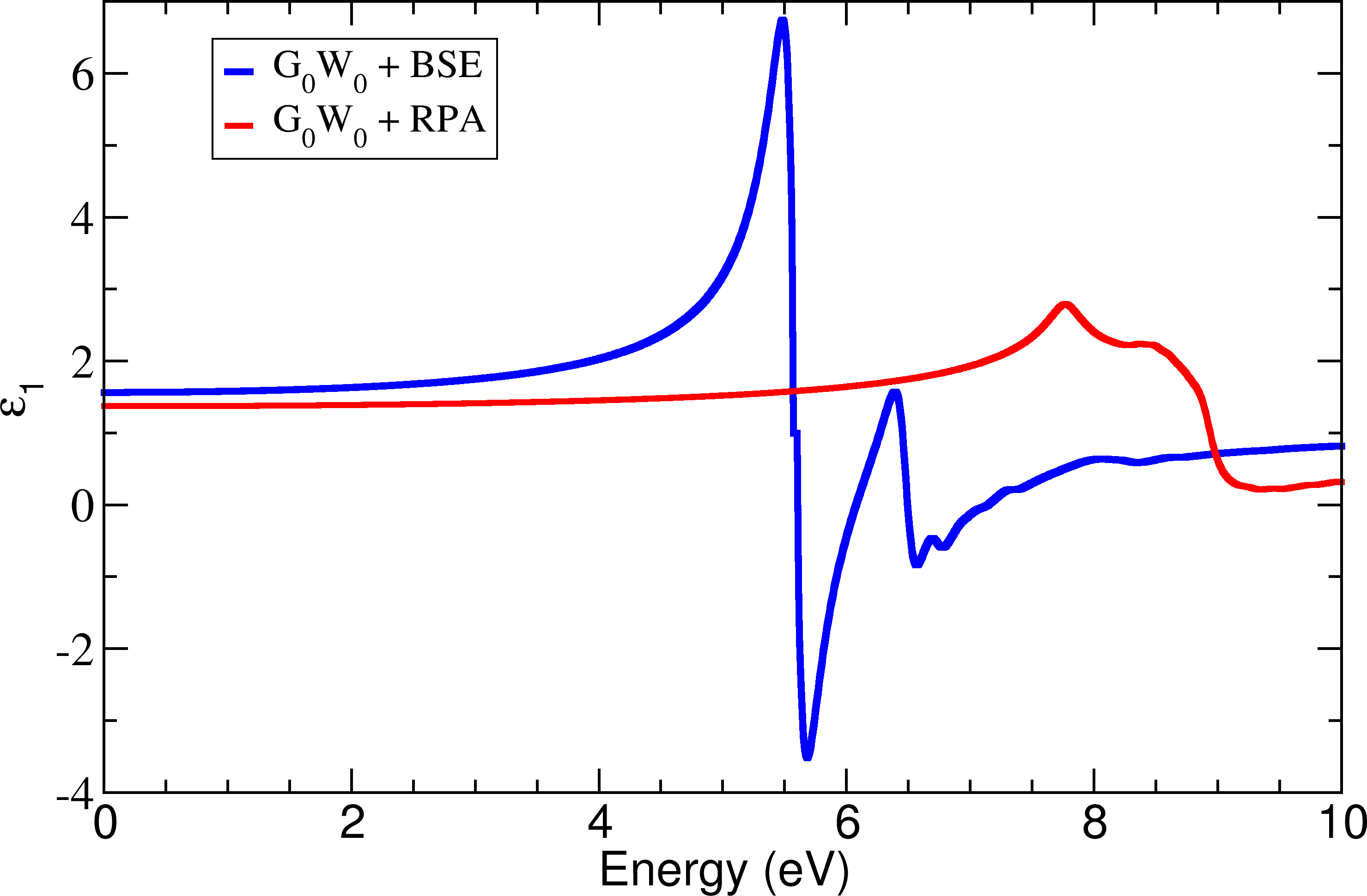
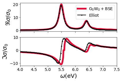
Fig. 2 shows the imaginary part of the dielectric function calculated by BSE, done on top of a calculation with a grid of -points. The convergence of the band structure with a particular grid of -points does not imply that BSE will be converged with the same grid. An interpolation with a fine grid of -points was needed to achieve convergence. Fig. 2 also shows the imaginary part of dielectric function without excitonic effects. The first peak has an energy of 5.58 eV and the second peak has an energy of 6.48 eV. In Table 3 we summarize the gap values of the band structure, the optical gap and the excitonic binding energy. Fig. 3 shows the real part of the dielectric function calculated with and without excitonic effects.
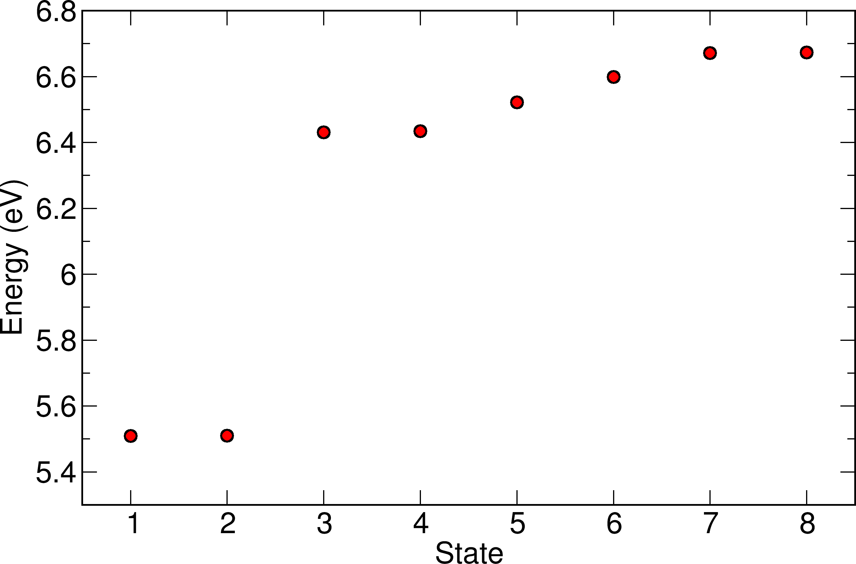
We also calculated the eigenvalues of the two particle states. Figure 4 shows the energies of the 8 lowest energy excitonic states. From now we label each state by the corresponding energy in an ascending order. The pairs of states (1,2), (3,4), and (7,8) are degenerate. States 1 and 2 are the degenerated ground state. We plot the probability density obtained from the BSE for these eight excitonic states in Fig. 5. These plots show the probability to find an electron at position if the hole is located at . We set the hole localized slightly above the nitrogen atom. The results were calculated using a coarse grid of -points and a BSE interpolation of -points. It can be noticed the complementarity of the degenerate states. For instance, if one adds the probability density of states 3 and 4, the symmetry of the lattice is recovered. And the same can be seen for the other degenerate states. The work of Ref. Galvani et al., 2016 has also studied the excitonic states. Their results are in good agreement with the ones obtained from this work.
1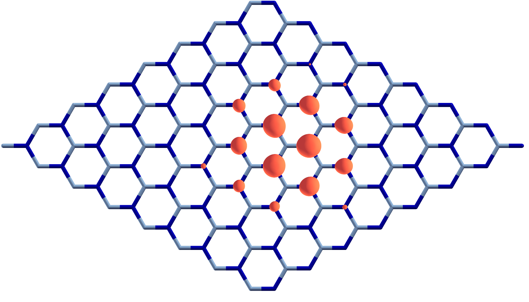
|
2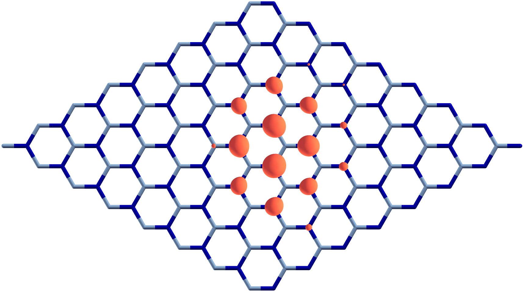
|
3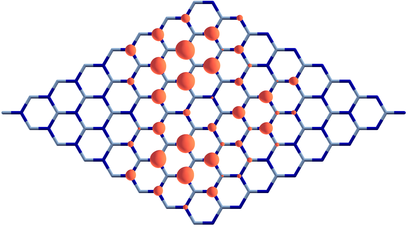
|
4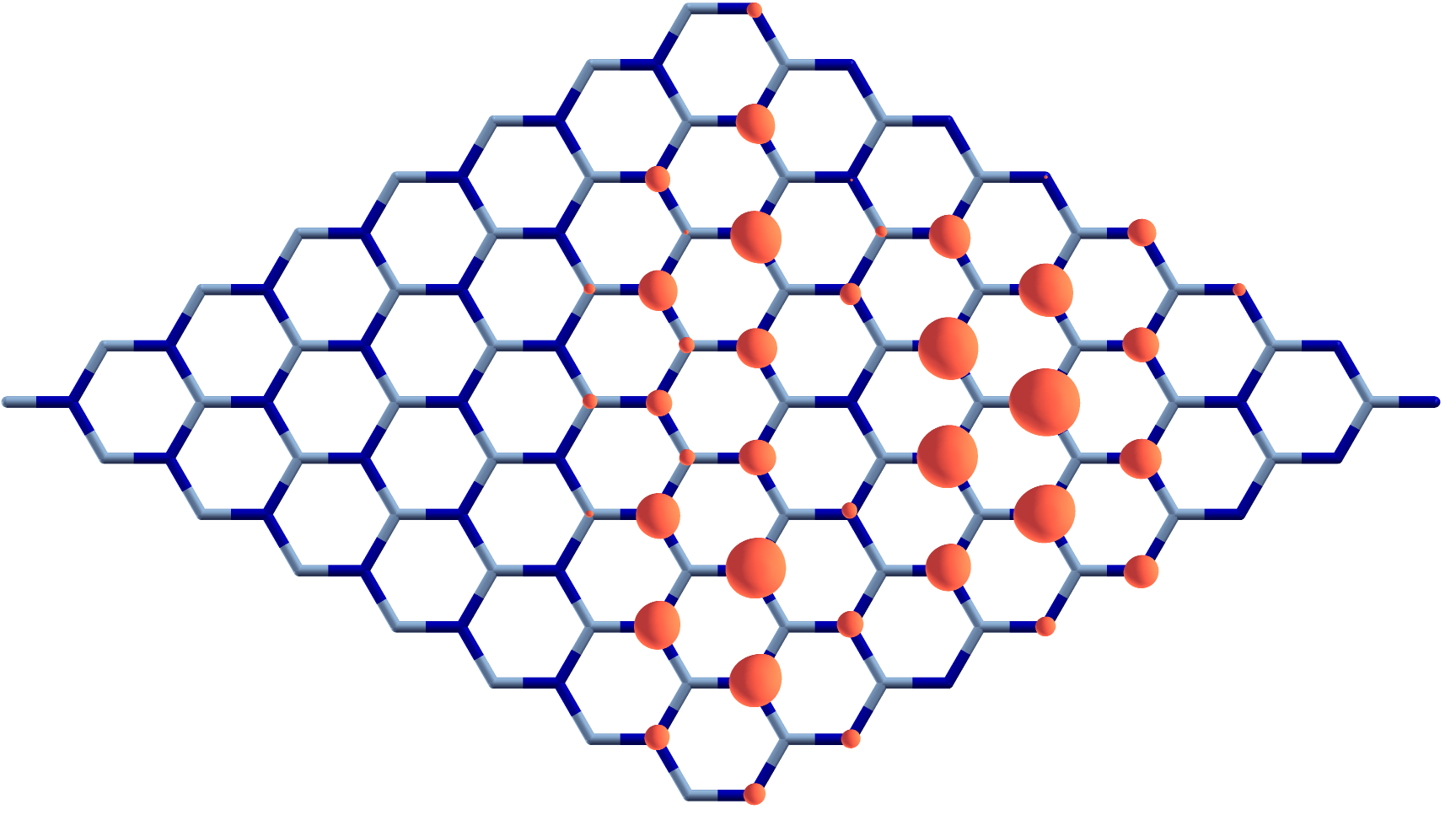
|
5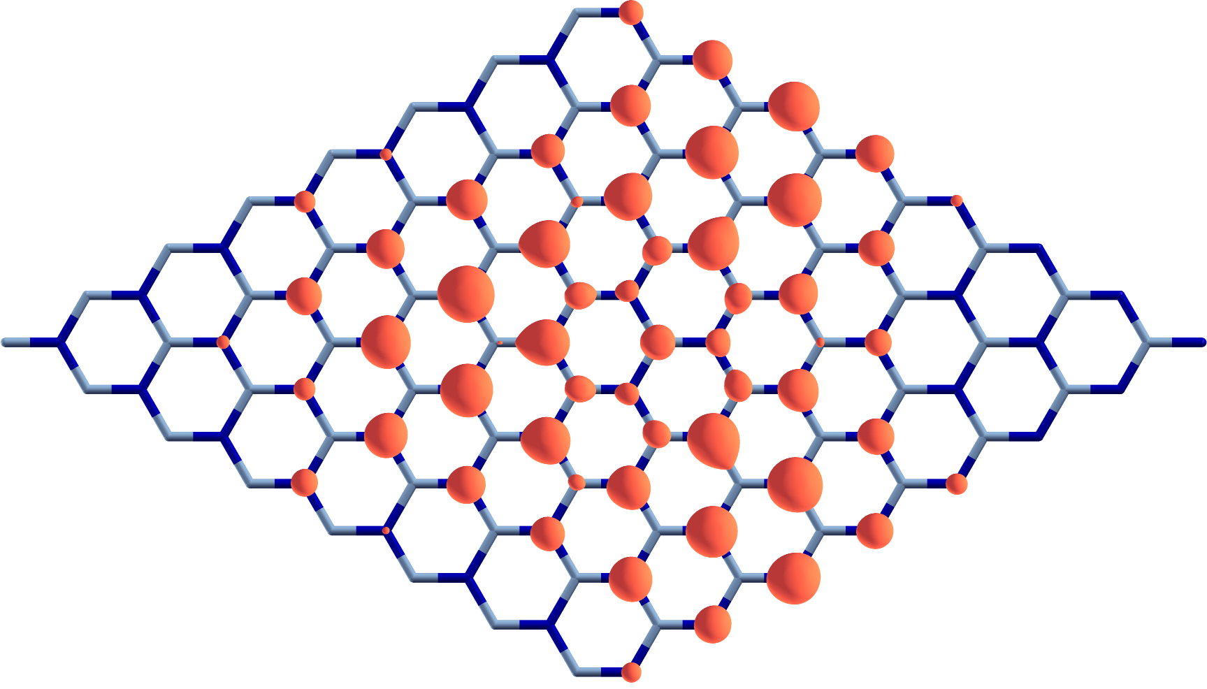
|
6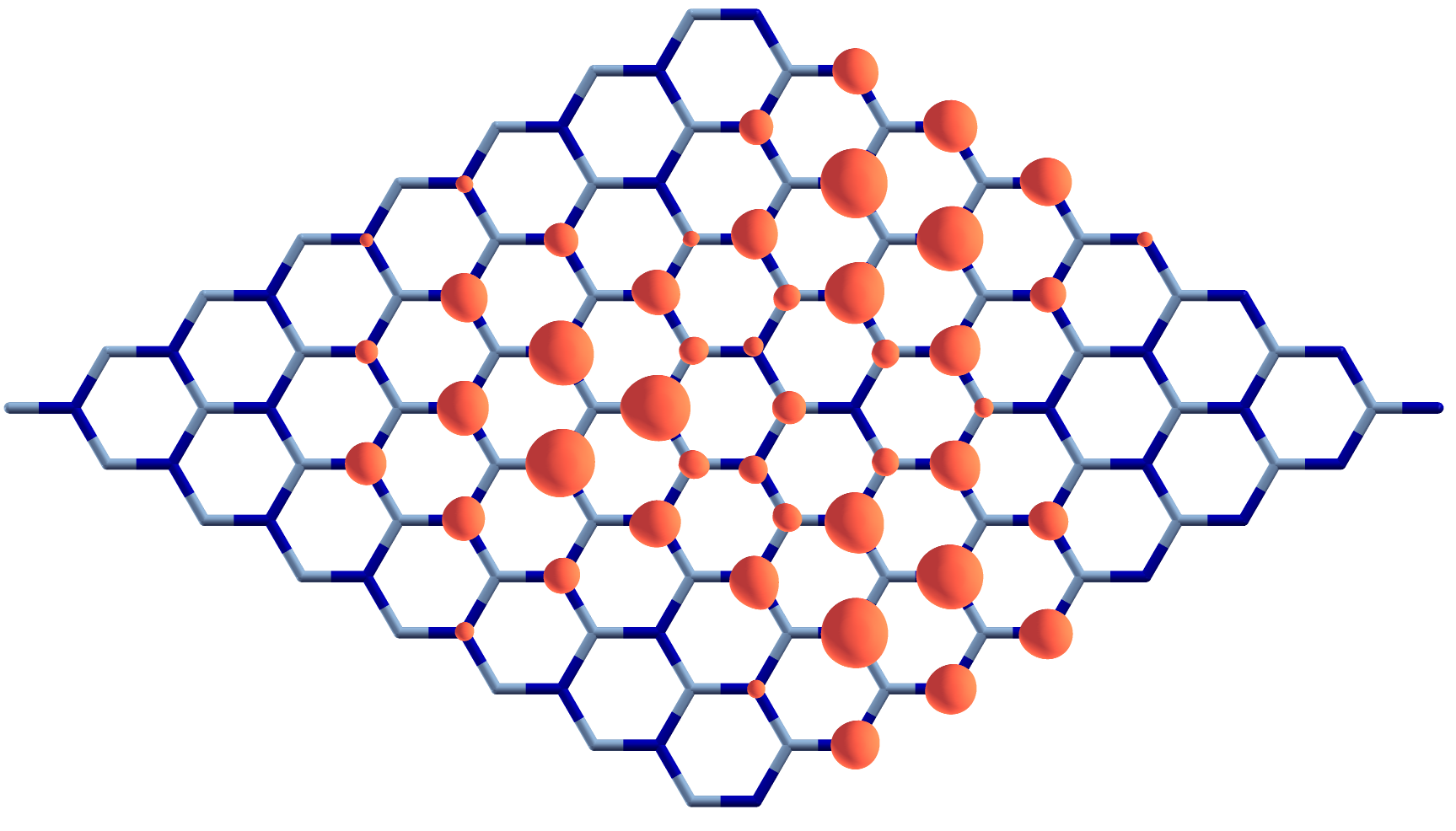
|
7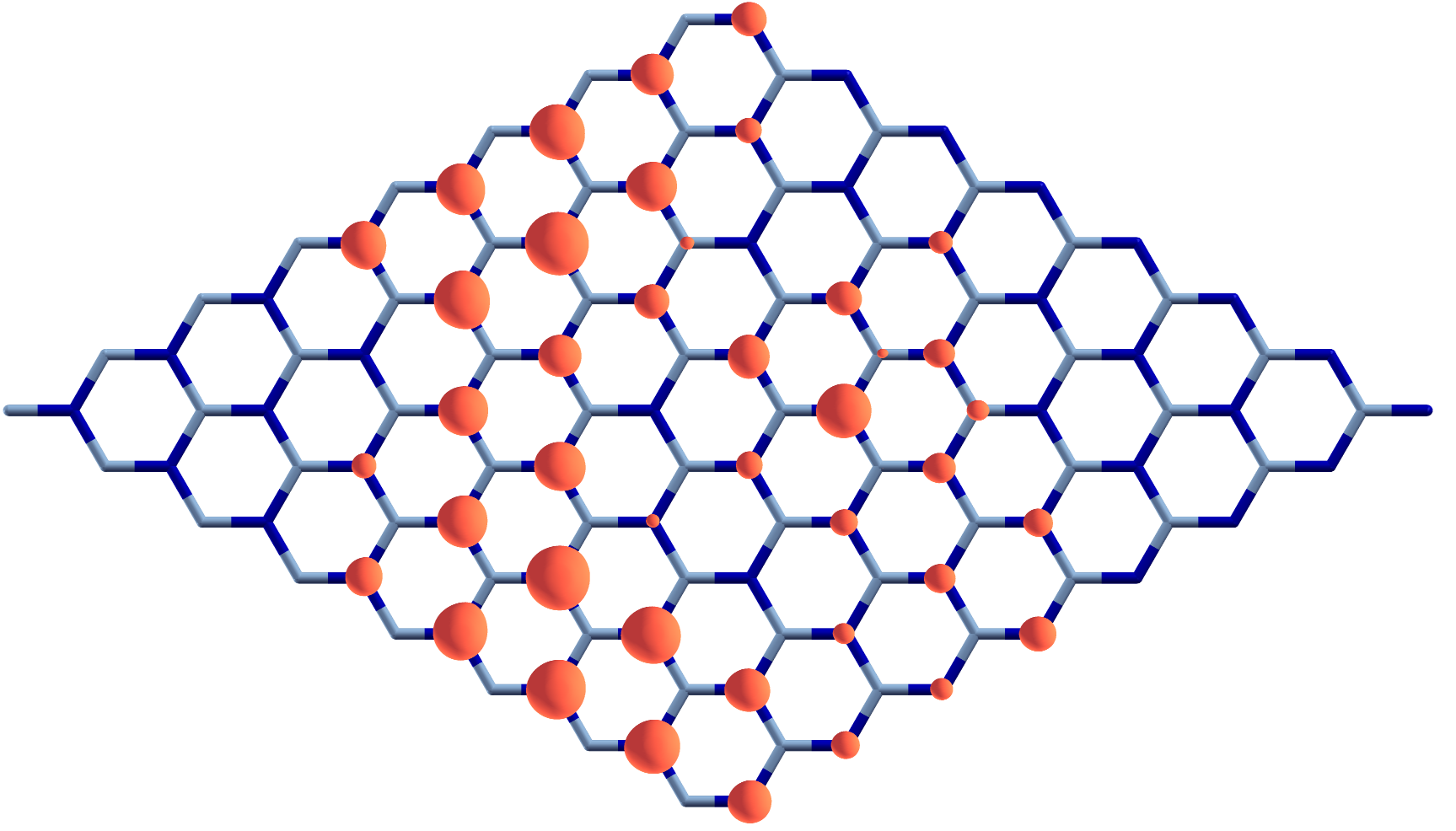
|
8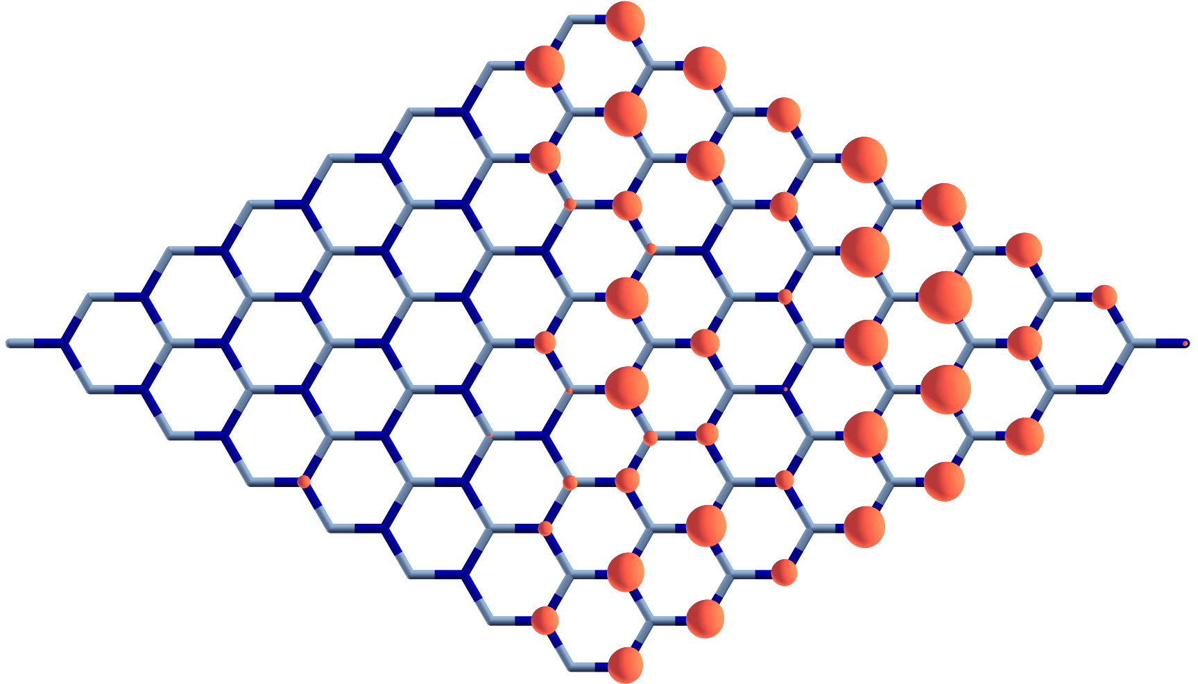
|
IV BSE in the equation of motion formalism and the Elliot formula
In this section we will follow the approach of the equation of motion derived in Ref. Chaves et al., 2017 and detailed in the Appendix A. The formalism is grounded on the calculation of the expected value of the polarization operator after we introduce an external electric field of intensity and frequency that couples with the electron gas in the 2D material. The optical conductivity and other properties can be obtained from the macroscopic relations. The starting point of our model is an effective Dirac hamiltonian,Ribeiro and Peres (2011) that can be obtained from a power series expansion of the tight-binding hamiltonian. The electron-electron interaction for a 2D material is given by the Keldysh potential.Cudazzo et al. (2011) This effective model only considers the top valence band and the bottom conductance band.
From the equation of motion we derive the following BSE:
| (3) |
where , is the interband transition amplitude, is the transition energy renormalized by the exchange self-energy and is a term that renormalizes the Rabi-Frequency, is the dipole matrix element and is the occupation difference, given by the Fermi-Dirac distribution. See Appendix A for more details.
From the homogeneous part of Eq. (3) we can obtain the exciton energies and the wave functions. Using the procedure explained in Ref. Chaves et al., 2017, we can obtain the corresponding Elliot formula for the optical conductivity:
| (4) |
where labels the exciton state, is the exciton linewidth, the exciton energy, the corresponding exciton weight and . Fig. 6 shows that the +BSE described in section III fits well to the Elliot formula, with a very good agreement in the real part and a small shift in the imaginary part. The energies and weights of the fit for the +BSE and the equation of motion method are compared in table 6. We use the parameters from Ref. Ribeiro and Peres, 2011: Å, eV , eV. The Keldysh potential parameter was calculated in Ref. Galvani et al., 2016 to be Å. We can see a excellent agreement between the exciton energies of both methods. The difference in the weights can be explained by the oversimplification of the Dirac hamiltonian used for the Elliot formula and consequently the less accurate dipole matrix elements that enter their calculation.
| (eV) | (eV) | |||
|---|---|---|---|---|
| +BSE | 5.48 | 0.088 | 6.41 | 0.027 |
| Eq. of Motion | 5.52 | 0.354 | 6.53 | 0.045 |
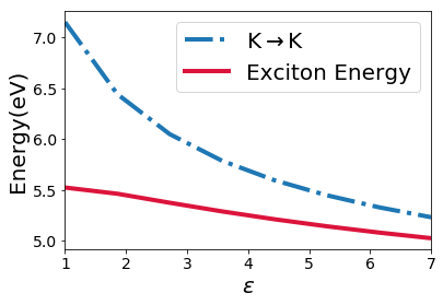
Finally, we used the equation of motion to predict the behavior of the exciton energy and the KK transition energy as a function of the environment dielectric constant. The result can be seen in Fig. 7. There is a strong decrease in the KK transition energy and an almost linear behavior, also decreasing, of the first exciton energy as the external dielectric constant increases. This effect is simple to understand, since a large dielectric constant screens more effectively the electron-electron interaction.
V Exciton-Polaritons
In this section we discuss the exciton-polariton modes in 2D hBN. Those modes are electromagnetic evanescent waves along the direction perpendicular to the hBN sheet. We assume that the hBN monolayer is cladded between two uniform, isotropic media with dielectric constants and and that the hBN sheet is in the -plane. So the electromagnetic mode is evanescent in the axis and proportional to . The modes can be classified as transverse magnetic or transverse electric (TM/TE).
The dispersion relation for the TM mode is given by the solution given in Ref. Bludov et al., 2013:
| (5) |
and for the TE mode:
| (6) |
with the hBN optical conductivity and:
| (7) |
where is the exciton-polariton in-plane wavevector and is the velocity of light in vacuum. We shall consider the simplest case of . A rule of thumb is that when ( ) TM (TE) modes are supported.
V.1 Complex Complex
First, we note that both Eqs. (5) and (6) are complex. Therefore, for a given () real, the solution will be a complex (). Each of these approaches (complex or complex ) lead to different dispersion relations for the exciton-polaritons as discussed elsewhere.Arakawa et al. (1973); Halevi and Fuchs (1984); Archambault et al. (2009); Conforti and Guasoni (2010); Udagedara et al. (2011) Both complex and complex approaches give the same results when an active media is used to balance the losses.Udagedara et al. (2011) The complex approach is suitable when the polariton is excited in a finite region of space with a monochromatic wave, while the complex approach is valid instead when the entire sample is excited by a pulsed light.Archambault et al. (2009)
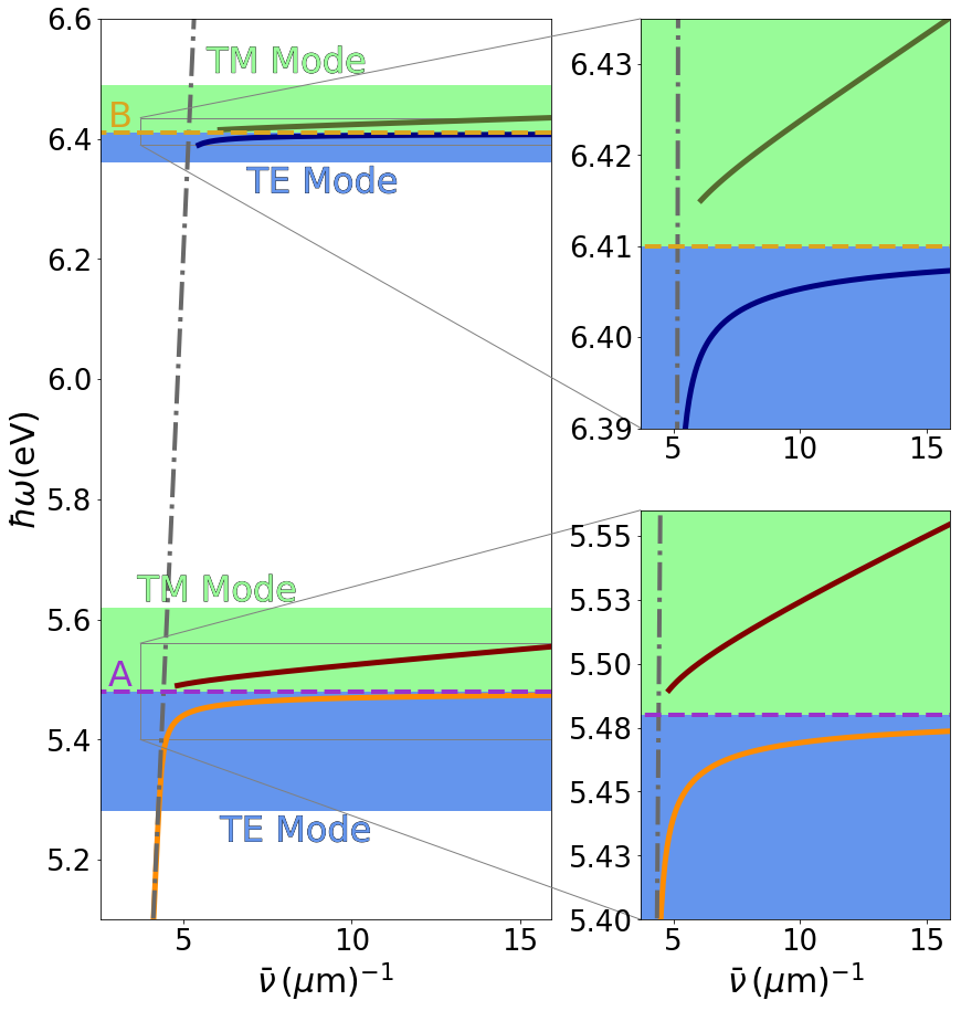
The dispersion relation for both the TE and TM modes in the complex approach was obtained by solving Eqs. (5) and (6) and using the Elliot formula (4) with the parameters of table (6) for the G0W0+BSE calculation and a damping of eV. The result is shown in Fig. 8, where and denote the first two excitonic energies. Both TE and TM modes can have a large localization (high or ) in this case. The TE mode has a flat dispersion relation that approaches the exciton energy as goes to infinity. As expected, the TM mode has a higher frequency than the exciton energy while the TE mode has a lower frequency. We point out that, and contrary to graphene, the TE mode presents a high degree of localization.
In the complex approach both excitons and support polaritons. This can be understood by examining Eq. (4). As approaches , the corresponding contribution to the optical conductivity diverges. This quantity can be infinitely negative or positive depending on the real part of the frequency approaching from the right or the left, supporting TM and TE modes respectively. Fig. 8 also shows that the electrostatic limit is approached near both exciton energies. In that limit the lifetime of the TM exciton-polariton can be calculated from (see Appendix B):
| (8) |
where is the fine-structure constant and is the contribution that arises from the background conductivity provenient from interband transitions and other excitonic states. For a negligible background , the exciton-polariton lifetime is proportional to the inverse of the exciton linewidth .
Next we shall consider the case of complex . There will be then a simple relation to obtain for a given frequency (assuming ):
| (9) |
with TM/TE and from Eqs. (5) and (6) we have:
| (10a) | |||
| (10b) | |||
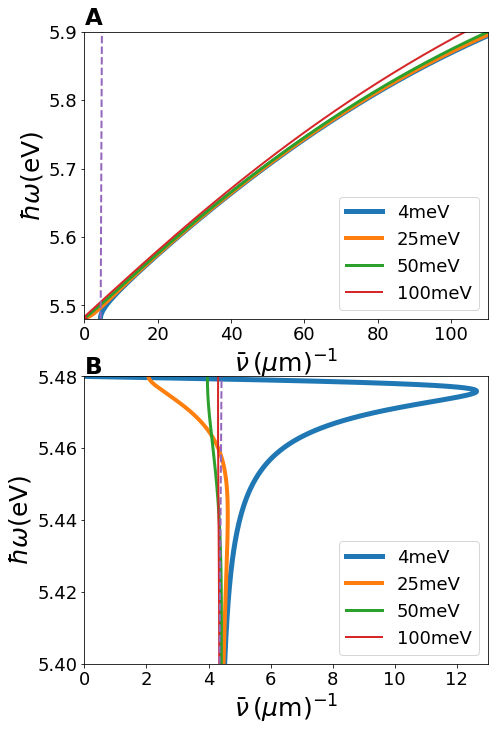
The condition for the existence of polaritons is . These equations allowed us to calculate the dispersion relation shown in Fig. 9 for several values of the damping constant . The dependence of the parameter of excitons was studied for WS2 in Ref. Cadiz et al. (2017) as function of temperature, showing that the linewidth decreases as the temperature decreases. From Fig. 9 we can see that the TE mode is strongly supressed except when the damping has the very low value of meV, close to the intrinsic line-width. The opposite happens for the TM mode, for which the dispersion relation is almost insensitive to the damping .
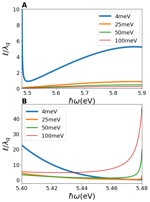
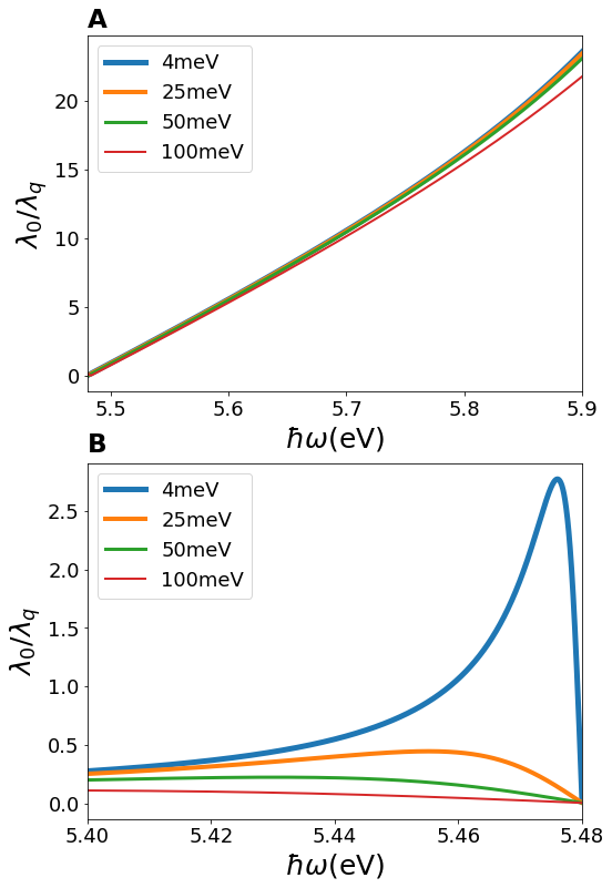
An important figure of merit is the ratio of the propagation length to the exciton wavelength , as it indicates if a polariton can propagate before extinction, that is shown in Fig. 10 for several values of . The TM mode is highly supressed except for the very low meV, while the TE mode has higher propagation rate and two different qualitative behaviors. For larger , the propagation rate increases with the frequency while the opposite happens for meV. A better understanding of this behavior can be achieved if we consider the confinement ratio , with being the wavelength of the free-radiation (see Figure 11). The confinement of the TM modes increases with increasing frequency and have a negligible dependence. On the other hand, the TE modes are poorly confined, with the confinement going to zero faster with increasing . This explains the large propagation rate in this case: the poorly confined field is essentially attenuated free radiation, i.e., there are no more excitons being excited, but the radiation field is attenuated by the material free charges.
The overall conclusion is that 2D hBN is a good platform for exciton-polaritons when we consider the complex approach for both TM and TE modes. In the complex approach, the results show that exciton-polariton can be observed only for meV.
V.2 UV radiation mirror
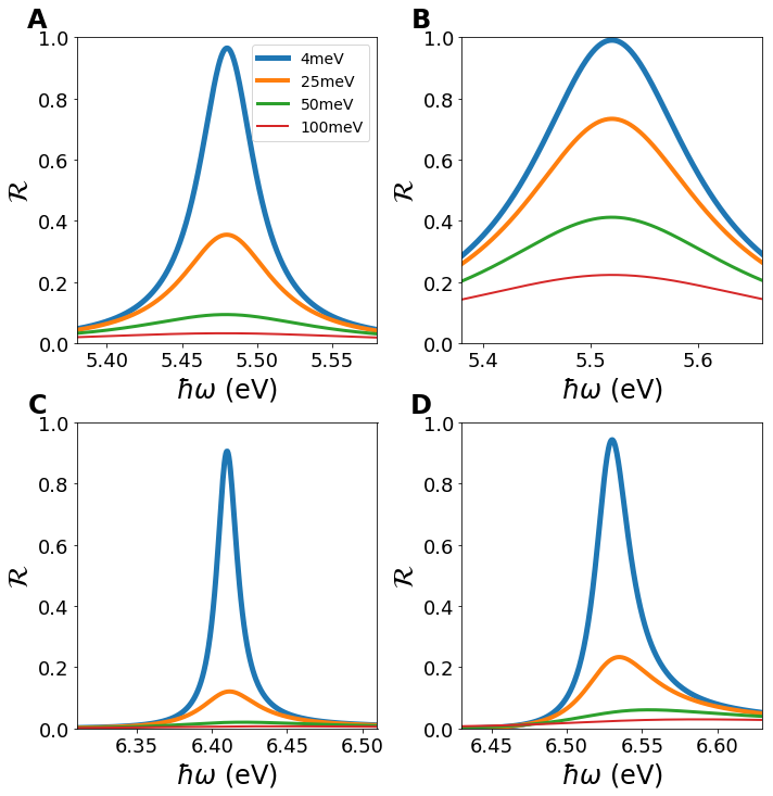
It was pointed out recently that excitons in MoSe2 can lead to very high reflection of electromagnetic radiation Back et al. (2018); Scuri et al. (2018). In this section we show that the same occurs with hBN, but in a different spectral range. We consider a free-standing hBN monolayer. In this case the reflection is given by:Gonçalves and Peres (2016)
| (11) |
where , is the fine structure constant and . Fig. 12 shows that the reflection can reach almost 100 for the value meV at the exciton energy. This is a consequence of the very high weights for hBN that appears in the Elliot formula (see table 6). We emphasize that those results are for a free-standing hBN sheet. The value can be controlled by the temperature as discussed in the sections before. As shown in Fig. 7, the exciton energy and therefore the reflection peak can be controlled by varying the external dielectric constant.
VI Conclusion
We calculated the band structure of 2D hexagonal boron nitride using DFT and the approximation. Then the Bethe-Salpeter equation was used to determine the excitonic energies of hBN. We determined the values of the band gap, optical gap, excitonic binding energies using a first principles approach. The results are in very good agreement with the ones obtained using a very different approach, namelly the equation of motion formalism and the Elliot formula, which are also presented in this paper. This latter formalism allowed us to study the optical properties for both the TM and TE modes. Our results show that 2D hBN is a good candidate to polaritonics in the UV range. We also show that a single layer h-BN can act as an almost perfect mirror for ultraviolet electromagnetic radiation.
Acknowledgments
R.M.R. and N.M.R.P. acknowledge support from the European Commission through the project “Graphene-Driven Revolutions in ICT and Beyond" (Ref. No. 785219), COMPETE2020, PORTUGAL2020, FEDER and the Portuguese Foundation for Science and Technology (FCT) through project PTDC/FIS-NAN/3668/2014 and in the framework of the Strategic Financing UID/FIS/04650/2013.
References
- Bao et al. (2016a) J. Bao, K. Jeppson, M. Edwards, Y. Fu, L. Ye, X. Lu, and J. Liu, Electronic Materials Letters 12, 1 (2016a).
- Bao et al. (2016b) J. Bao, M. Edwards, S. Huang, Y. Zhang, Y. Fu, X. Lu, Z. Yuan, K. Jeppson, and J. Liu, Journal of Physics D: Applied Physics 49, 265501 (2016b).
- Amorim et al. (2016) B. Amorim, R. M. Ribeiro, and N. M. R. Peres, Phys. Rev. B 93, 235403 (2016).
- Banszerus et al. (2016) L. Banszerus, M. Schmitz, S. Engels, M. Goldsche, K. Watanabe, T. Taniguchi, B. Beschoten, and C. Stampfer, Nano Letters 16, 1387 (2016), pMID: 26761190, http://dx.doi.org/10.1021/acs.nanolett.5b04840 .
- Jung et al. (1) J. Jung, A. M. DaSilva, A. H. MacDonald, and S. Adam, Nature Communications 6, 1 (1), arXiv:1403.0496 .
- Duan et al. (2016) J. Duan, X. Wang, X. Lai, G. Li, K. Watanabe, T. Taniguchi, M. Zebarjadi, and E. Y. Andrei, Proceedings of the National Academy of Sciences 113, 14272 (2016), http://www.pnas.org/content/113/50/14272.full.pdf .
- Li et al. (2016) X. Li, S. Sundaram, Y. El Gmili, T. Ayari, R. Puybaret, G. Patriarche, P. L. Voss, J. P. Salvestrini, and A. Ougazzaden, Crystal Growth & Design 16, 3409 (2016), http://dx.doi.org/10.1021/acs.cgd.6b00398 .
- Vuong et al. (2017) T. Q. P. Vuong, G. Cassabois, P. Valvin, E. Rousseau, A. Summerfield, C. J. Mellor, Y. Cho, T. S. Cheng, J. D. Albar, L. Eaves, C. T. Foxon, P. H. Beton, S. V. Novikov, and B. Gil, 2D Materials 4, 021023 (2017).
- Basov et al. (2016) D. Basov, M. Fogler, and F. G. de Abajo, Science 354, aag1992 (2016).
- Low et al. (2017) T. Low, A. Chaves, J. D. Caldwell, A. Kumar, N. X. Fang, P. Avouris, T. F. Heinz, F. Guinea, L. Martin-Moreno, and F. Koppens, Nature materials 16, 182 (2017).
- Watanabe et al. (2011) Y. Watanabe, W. Inami, and Y. Kawata, Journal of Applied Physics 109, 023112 (2011).
- Mattiucci et al. (2012) N. Mattiucci, G. D’Aguanno, H. O. Everitt, J. V. Foreman, J. M. Callahan, M. C. Buncick, and M. J. Bloemer, Optics express 20, 1868 (2012).
- McMahon et al. (2013) J. M. McMahon, G. C. Schatz, and S. K. Gray, Physical Chemistry Chemical Physics 15, 5415 (2013).
- Yang et al. (2013) Y. Yang, J. M. Callahan, T.-H. Kim, A. S. Brown, and H. O. Everitt, Nano letters 13, 2837 (2013).
- Maidecchi et al. (2013) G. Maidecchi, G. Gonella, R. Proietti Zaccaria, R. Moroni, L. Anghinolfi, A. Giglia, S. Nannarone, L. Mattera, H.-L. Dai, M. Canepa, et al., Acs Nano 7, 5834 (2013).
- Ross and Schatz (2014) M. B. Ross and G. C. Schatz, The Journal of Physical Chemistry C 118, 12506 (2014).
- Watson et al. (2015) A. M. Watson, X. Zhang, R. Alcaraz de La Osa, J. M. Sanz, F. González, F. Moreno, G. Finkelstein, J. Liu, and H. O. Everitt, Nano letters 15, 1095 (2015).
- Alcaraz de la Osa et al. (2015) R. Alcaraz de la Osa, J. Sanz, A. Barreda, J. Saiz, F. González, H. Everitt, and F. Moreno, The Journal of Physical Chemistry C 119, 12572 (2015).
- Gutierrez et al. (2016) Y. Gutierrez, D. Ortiz, J. M. Sanz, J. M. Saiz, F. Gonzalez, H. O. Everitt, and F. Moreno, Optics express 24, 20621 (2016).
- Gutiérrez et al. (2018) Y. Gutiérrez, R. Alcaraz de la Osa, D. Ortiz, J. M. Saiz, F. González, and F. Moreno, Applied Sciences 8, 64 (2018).
- Kumamoto et al. (2011) Y. Kumamoto, A. Taguchi, N. I. Smith, and S. Kawata, Biomedical optics express 2, 927 (2011).
- Knight et al. (2012) M. W. Knight, L. Liu, Y. Wang, L. Brown, S. Mukherjee, N. S. King, H. O. Everitt, P. Nordlander, and N. J. Halas, Nano letters 12, 6000 (2012).
- Nagashima et al. (1995) A. Nagashima, N. Tejima, Y. Gamou, T. Kawai, and C. Oshima, Physical Review B 51, 4606 (1995).
- Hedin (1965) L. Hedin, Phys. Rev. 139, A796 (1965).
- Hedin and Lundqvist (1970) L. Hedin and S. Lundqvist, Solid State Physics 23, 1 (1970).
- Salpeter and Bethe (1951) E. E. Salpeter and H. A. Bethe, Phys. Rev. 84, 1232 (1951).
- Albrecht et al. (1998) S. Albrecht, L. Reining, R. Del Sole, and G. Onida, Phys. Rev. Lett. 80, 4510 (1998).
- Blase et al. (1995) X. Blase, A. Rubio, S. G. Louie, and M. L. Cohen, Phys. Rev. B 51, 6868 (1995).
- Sahin et al. (2009) H. Sahin, S. Cahangirov, M. Topsakal, E. Bekaroglu, E. Akturk, R. T. Senger, and S. Ciraci, Phys. Rev. B 80, 155453 (2009).
- Berseneva et al. (2013) N. Berseneva, A. Gulans, A. V. Krasheninnikov, and R. M. Nieminen, Phys. Rev. B 87, 035404 (2013).
- Cudazzo et al. (2016) P. Cudazzo, L. Sponza, C. Giorgetti, L. Reining, F. Sottile, and M. Gatti, Phys. Rev. Lett. 116, 066803 (2016).
- Wirtz et al. (2006) L. Wirtz, A. Marini, and A. Rubio, Phys. Rev. Lett. 96, 126104 (2006).
- Galvani et al. (2016) T. Galvani, F. Paleari, H. P. C. Miranda, A. Molina-Sánchez, L. Wirtz, S. Latil, H. Amara, and F. Ducastelle, Phys. Rev. B 94, 125303 (2016).
- Ferreira and Ribeiro (2017) F. Ferreira and R. M. Ribeiro, Phys. Rev. B 96, 115431 (2017).
- Shih et al. (2010) B.-C. Shih, Y. Xue, P. Zhang, M. L. Cohen, and S. G. Louie, Phys. Rev. Lett. 105, 146401 (2010).
- Berger et al. (2010) J. A. Berger, L. Reining, and F. Sottile, Phys. Rev. B 82, 041103 (2010).
- Deslippe et al. (2012) J. Deslippe, G. Samsonidze, D. A. Strubbe, M. Jain, M. L. Cohen, and S. G. Louie, Computer Physics Communications 183, 1269 (2012).
- Hybertsen and Louie (1986) M. S. Hybertsen and S. G. Louie, Phys. Rev. B 34, 5390 (1986).
- Rohlfing and Louie (2000) M. Rohlfing and S. G. Louie, Phys. Rev. B 62, 4927 (2000).
- Giannozzi et al. (2009) P. Giannozzi, S. Baroni, N. Bonini, M. Calandra, R. Car, C. Cavazzoni, D. Ceresoli, G. L. Chiarotti, M. Cococcioni, I. Dabo, A. Dal Corso, S. de Gironcoli, S. Fabris, G. Fratesi, R. Gebauer, U. Gerstmann, C. Gougoussis, A. Kokalj, M. Lazzeri, L. Martin-Samos, N. Marzari, F. Mauri, R. Mazzarello, S. Paolini, A. Pasquarello, L. Paulatto, C. Sbraccia, S. Scandolo, G. Sclauzero, A. P. Seitsonen, A. Smogunov, P. Umari, and R. M. Wentzcovitch, Journal of Physics: Condensed Matter 21, 395502 (19pp) (2009).
- Perdew et al. (1996) J. P. Perdew, K. Burke, and M. Ernzerhof, Phys. Rev. Lett. 77, 3865 (1996).
- Monkhorst and Pack (1976) H. J. Monkhorst and J. D. Pack, Phys. Rev. B 13, 5188 (1976).
- Chaves et al. (2017) A. Chaves, R. Ribeiro, T. Frederico, and N. Peres, 2D Materials 4, 025086 (2017).
- Ribeiro and Peres (2011) R. M. Ribeiro and N. M. R. Peres, Phys. Rev. B 83, 235312 (2011).
- Cudazzo et al. (2011) P. Cudazzo, I. V. Tokatly, and A. Rubio, Physical Review B 84, 085406 (2011).
- Bludov et al. (2013) Y. V. Bludov, A. Ferreira, N. Peres, and M. Vasilevskiy, International Journal of Modern Physics B 27, 1341001 (2013).
- Arakawa et al. (1973) E. Arakawa, M. Williams, R. Hamm, and R. Ritchie, Physical Review Letters 31, 1127 (1973).
- Halevi and Fuchs (1984) P. Halevi and R. Fuchs, Journal of Physics C: Solid State Physics 17, 3869 (1984).
- Archambault et al. (2009) A. Archambault, T. V. Teperik, F. Marquier, and J.-J. Greffet, Physical Review B 79, 195414 (2009).
- Conforti and Guasoni (2010) M. Conforti and M. Guasoni, JOSA B 27, 1576 (2010).
- Udagedara et al. (2011) I. B. Udagedara, I. D. Rukhlenko, and M. Premaratne, Physical Review B 83, 115451 (2011).
- Cadiz et al. (2017) F. Cadiz, E. Courtade, C. Robert, G. Wang, Y. Shen, H. Cai, T. Taniguchi, K. Watanabe, H. Carrere, D. Lagarde, et al., Physical Review X 7, 021026 (2017).
- Back et al. (2018) P. Back, S. Zeytinoglu, A. Ijaz, M. Kroner, and A. Imamoğlu, Physical Review Letters 120, 037401 (2018).
- Scuri et al. (2018) G. Scuri, Y. Zhou, A. A. High, D. S. Wild, C. Shu, K. De Greve, L. A. Jauregui, T. Taniguchi, K. Watanabe, P. Kim, et al., Physical Review Letters 120, 037402 (2018).
- Gonçalves and Peres (2016) P. A. D. Gonçalves and N. M. R. Peres, An Introduction to Graphene Plasmonics (World Scientific, 2016).
- Rodin et al. (2014) A. S. Rodin, A. Carvalho, and A. H. Castro Neto, Phys. Rev. B 90, 075429 (2014).
Appendix A Equation of motion formalism
The total hamiltonian that we consider in the equation of motion approach is where we have the Dirac hamiltonian:
| (12) |
the dipole interaction hamiltonian:
| (13) |
and the electron-electron interaction:
| (14) |
where we used the field operator:
| (15) |
with the eigenvector of :
| (16) |
and eigenvalues:
| (17) |
We note that the electron-electron interaction for charges confined in a 2D material is given by the Keldysh potential:Cudazzo et al. (2011),Rodin et al. (2014)
| (18) |
The expected value of the polarization operator for the 2D Dirac equation can be written as:
| (19) |
takes into account the spin and valley degeneracy, labels the valence () or the conduction () band. The dipole matrix element is:
| (20) |
The interband transition amplitude is defined as:
| (21) |
where ( ) is the creation (annihilation) operator in band in the Heisenberg picture.
As explained in Ref. Chaves et al., 2017, from the equation of motion for the transition amplitude we can derive the following Bethe-Salpeter Equation:
| (22) |
where is the renormalized transition energy:
| (23) |
where the exchange self-energy is included as
| (24) |
where are defined in Eq. (26). We define where is the Fermi-Dirac distribution and which gives us the difference in occupation between valence and conductance bands for a vertical transition. Finally, the integral term is:
| (25) |
The homogeneous part of equation 22, obtained by setting , can be used to calculate the excitons wavefunctions and energies. From the inhomogeneous solution of 22, the macroscopic polarization can be calculated using Eq. 19 and from there it follows the optical conductivity, permittivity and absorbance.
The overlap of four wavefunctions is given by the function:
| (26) |
Appendix B Exciton in the polariton eletrostatic limit
In the electrostatic limit the TM exciton-polariton equation read as:
| (27) |
with the solution:
| (28) |
where can be a complex quantity, the polariton lifetime is given by , and:
| (29) |
from (28) we can see that excitons-polaritons always exist in TMD’s systems. For the parameters considered, , so the exciton-polariton will always exists for energies higher than the exciton energy. This term also defines the exciton-polariton bandwidth, for :
| (30) |