Performance of CMOS pixel sensor prototypes in ams H35 and aH18 technology for the ATLAS ITk upgrade111© 2018. This manuscript version is made available under the CC-BY-NC-ND 4.0 license.
Abstract
Pixel sensors based on commercial high-voltage CMOS processes are an exciting technology that is considered as an option for the outer layer of the ATLAS inner tracker upgrade at the High Luminosity LHC. Here, charged particles are detected using deep n-wells as sensor diodes with the depleted region extending into the silicon bulk. Both analog and digital readout electronics can be added to achieve different levels of integration up to a fully monolithic sensor. Small scale prototypes using the ams CMOS technology have previously demonstrated that it can achieve the required radiation tolerance of and detection efficiencies above . Recently, large area prototypes, comparable in size to a full sensor, have been produced that include most features required towards a final design: the H35demo prototype produced in ams H35 technology that supports both external and integrated readout and the monolithic ATLASPix1 pre-production design produced in ams aH18 technology. Both chips are based on large fill-factor pixel designs, but differ in readout structure. Performance results for H35DEMO with capacitively-coupled external readout and first results for the monolithic ATLASPix1 are shown.
keywords:
ATLAS ITk upgrade, High Luminosity LHC, Silicon pixel sensor, Monolithic active pixel sensor, CMOS, HV-MAPS1 Introduction
Tracking detectors at future colliders have to fulfil increasingly demanding requirements. Their environment will contain a higher density of tracks, at higher rate, with a higher radiation dose over their lifetime compared to current detectors. This necessitates high granularity detectors even far away from the interaction point and consequently large instrumented surface areas. The planned ATLAS Inner Tracker (ITk) upgrade [1, 2] is one such detector that is designed to withstand the environment at the planned high luminosity large hadron collider. Sensors for the outer layer of the ATLAS ITk pixel tracker have to cope with an integrated radiation dose of up to over its lifetime.
Silicon pixel detectors are the only technology that can provide the granularity, rate capability, and radiation hardness. Traditionally they are implemented as hybrid pixel sensors. Traversing particles generate free charges in a fully depleted passive sensor diode. Pixelated electrodes on the sensor are connected via bump-bonding to a dedicated readout chip. The readout chip contains both analog amplifiers and digital processing logic and handles the triggering and readout.
While this separation of concerns allows each component to be optimized separately it also introduces additional challenges. A large charge signal is required to generate a large enough voltage signal over the total capacitance of the sensor diode and the readout electronics. This necessitates a thick, fully depleted sensor diode with a high voltage bias to deplete it. As an example, the central modules used in the ATLAS IBL detector are built from thick planar sensors, with bias voltages foreseen to reach , bump-bonded to a thick readout chips [3]. The complexity of the production process, i.e. separate sensor and readout production and hybridization, can be a limiting factor to production capabilities. Yield factors compound and due to the many steps involved the production can not easily scale to large number of sensors and large instrumented surface areas.
Pixel sensors based on CMOS technology enable simpler devices with a reduced material budget by integrating some or all of the readout electronics directly into one chip. Commercial production enables cheap sensors with greatly simplified production complexity, suitable to instrument large surface areas with high granularity sensors.
In the remainder of this paper, basic concepts are introduced and different implementations of CMOS-based pixel sensors using ams technology are presented. Then, specific prototypes and the status of ongoing prototype evaluations are discussed.
2 ams CMOS prototypes
The ams technology is a set of commercial CMOS processes that are available in and structure sizes [4]. All processes can use nMOS and pMOS transistors and support high voltages of up to . High-resistivity substrates up to are also available.
Previous small-scale prototypes based on this technology used integrated amplifiers and comparators in combination with an external readout chip. They could be operated with efficiencies above for fluences up to using both neutron and proton irradiation [5], demonstrating the radiation hardness of this technology. Other small-scale prototypes demonstrated the feasibility of integrating different levels of readout logic onto the same chip [6, 7].
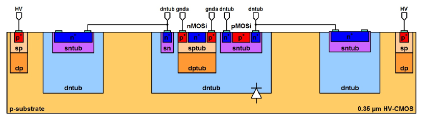
Two large-scale pixel sensor prototypes, H35DEMO and ATLASPix1, have been recently produced to show the viability of this technology for full-sized production sensors as an upgrade option for ATLAS ITk and to test different aspects of the technology. All prototypes are based on so-called large fill-factor designs. The large fill-factor refers to the size of the sensor diode compared to the pixel pitch. In these designs, the pixel electronics are located inside a deep n-type implant in a p-type substrate. The deep n-type implant and the substrate form the sensor diode that is depleted by applying a bias voltage. Usually bias from the top side is used; back-bias could also be employed but requires additional back-side processing. Figure 1 shows a cross-section of the pixel implants for the H35DEMO prototype along the large pitch direction. Here, three separate sensor diodes are connected together to reduce the total sensor capacitance while maintaining a homogeneous depletion. Figure 2 shows the equivalent pixel implants cross-section for the ATLASPix1 prototype. Due to a smaller size only a single diode implantation is used.
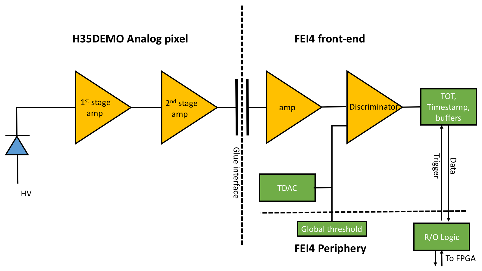
H35DEMO is produced in H35 technology with a total size of and a pixel pitch of [8]. It comprises four independent matrices: two monolithic matrices with integrated readout and two analog matrices that integrate only per-pixel amplifiers. On the first monolithic matrix each pixel contains amplifiers and comparator while on the second matrix only the amplifiers are located in the pixel and the comparator is located in the chip periphery. Evaluation results for the two monolithic matrices were previously reported by Cavallaro et al. [9] and Terzo et al. [10]. The analog matrices provide an amplified analog signal that is then readout by a capacitively coupled FE-I4 readout chip as shown in figure 3. The two analog matrices differ in the layout of their in-pixel electronics. Within each analog matrix there are different submatrices with additional small variations of the integrated electronics.
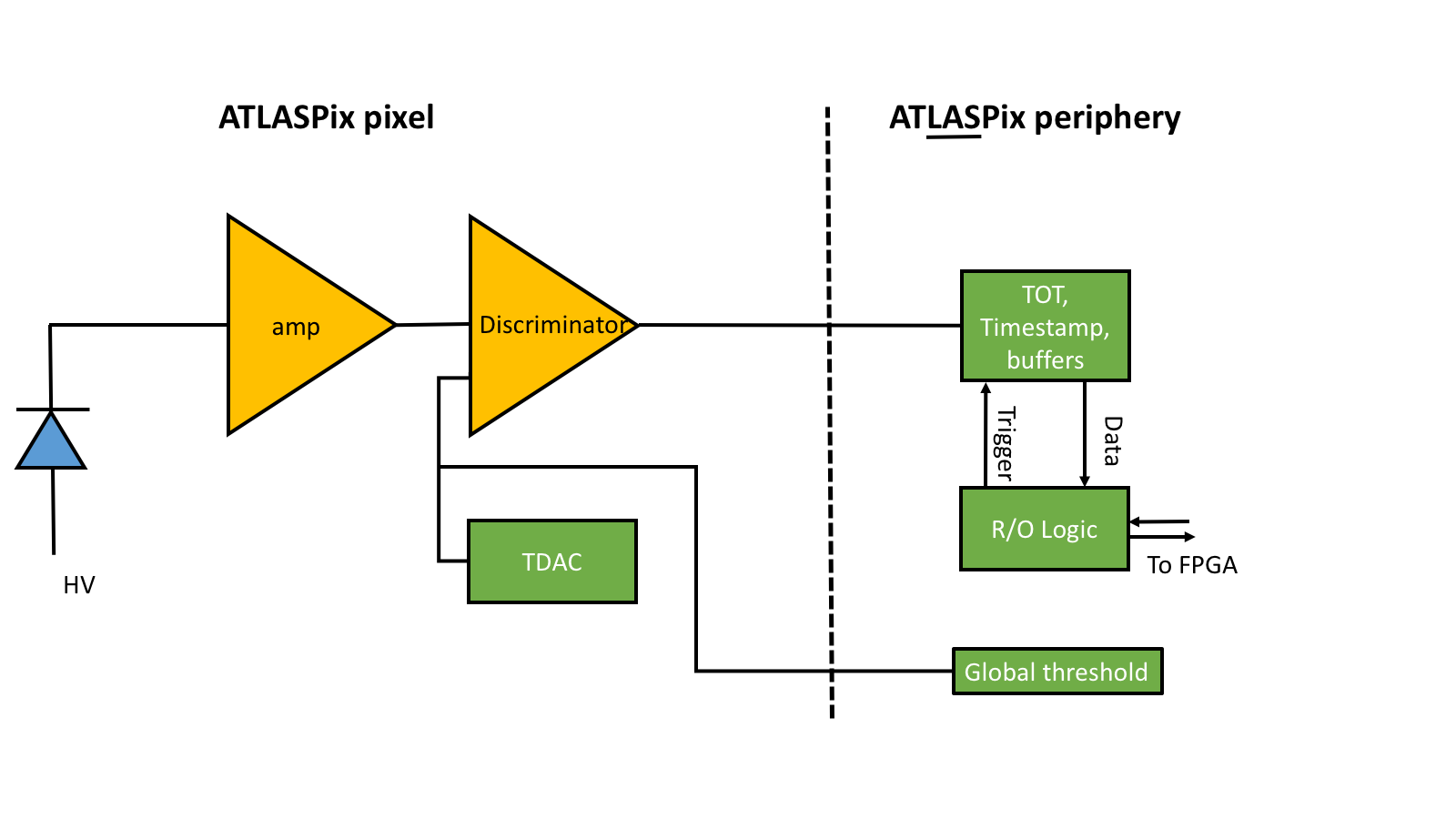
ATLASPix1 is a monolithic prototype with integrated readout logic and a total size of approximately produced in aH18 technology. It comprises three independent matrices — M2, Simple and IsoSimple — that differ in readout architecture and pixel pitch. M2 has a pixel pitch of and uses a triggered readout architecture. Simple and IsoSimple have a pixel pitch of and use an untriggered column-drain architecture. The IsoSimple matrix has an additional isolation p-well, as shown in figure 2, and use full CMOS transistor in its comparator logic. The Simple matrix only uses nMOS logic and misses the isolation p-well. As shown in figure 4, all matrices have the per-pixel amplifier and comparator located inside each pixel which are connected to additional logic in the digital periphery.
3 Beam tests
The operational performance of both prototypes was tested in beam test setups. Measurements with the H35DEMO were performed in spring 2017 at the Fermilab MTEST facility using the primary proton beam and in summer 2017 at the CERN north area beam facilities using a secondary mixed hadron beam. Measurements with the ATLASPix1 prototype were performed in October 2017 at the CERN north area facilities also using a secondary mixed hadron beam.
Reference tracks were measured using the Geneva beam telescope. It uses six ATLAS IBL modules with a pixel pitch of to measure particle positions [11]. The sensors are arranged in an optimized geometry with rotated and inclined planes to maximize charge sharing and enhance the resolution. The telescope and FE-I4-based devices-under-test are readout using the RCE/HSIO2 data acquisition system [11]. Triggers are provided by hit coincidences on the first and the last plane with a variable integration time between 8 and 16 time bins of .
The H35DEMO prototypes with capacitively coupled FE-I4 readout sensors can be read out directly using the RCE/HSIO2 system. The ATLASPix1 is operated with an independent data acquisition system based on a commercial Xilinx Nexys FPGA board in combination with a custom control and readout board developed at KIT. It is controlled via USB2 using a custom software. Integration into the telescope system is achieved via a trigger-busy scheme. The trigger signal from the telescope is used by the FPGA to write data only for triggered events into a separated stream. Synchronisation between the two systems happens offline based on trigger counting and timestamps.
Particle tracks are reconstructed with the Proteus reconstruction software [12] using only the data from the telescope planes. Proteus performs hit clustering, weighted center-of-gravity position, and detector alignment. Initial coarse alignment is based on hit correlations and subsequent fine alignment uses track residuals. Reconstructed track positions and the full reconstruction covariance matrix are propagated into the local system of the device-under-test and are then used to calculated residuals and efficiency.
4 H35DEMO results
A systematic evaluation of the performance of the two H35DEMO analog matrices has been performed. In this configuration only analog electronics, i.e. signal amplifiers and shapers, but no digital readout logic is integrated on the CMOS chip. It can therefore be used to test the performance of the sensor and the analog electronics independent of the readout logic by using the well-tested FE-I4 readout chip. Detailed evaluation results for the H35DEMO analog matrices have previously been reported by Benoit et al. [13]. Only a high-level overview is provided here to give the reader a full picture of all ams CMOS prototypes.
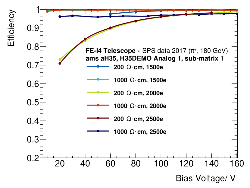
Figure 5 shows the resulting global efficiency measured for one submatrix of the first analog matrix for different device configurations as a function of the sensor bias voltage. The threshold quoted is the threshold set on the coupled FE-I4 readout chip. Since the initial signal is already amplified and shaped by the integrated amplifiers on the H35DEMO the effective threshold in terms of generated charge in the sensor is smaller. As expected, a clear dependence is seen on both substrate resistivity and threshold. A higher substrate resistivity leads to larger signal and therefore to a higher efficiency for the same threshold and bias. The same is true for lower threshold. For both shown substrate resistivities an operational region with efficiencies above can be found. The measured efficiency is comparable to or better than results from traditional hybrid modules with bump-bonded passive sensors and fulfil the efficiency requirement of for the outer layer of the ATLAS ITk upgrade [2].
5 ATLASPix1 results
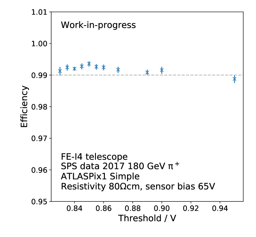
Given the availability of prototype samples and time constraints measurements could only be performed for the ATLASPix1 Simple matrix of one unirradiated sample with a substrate resistivity of . These measurements test both the analog performance of the sensor and the integrated readout logic.
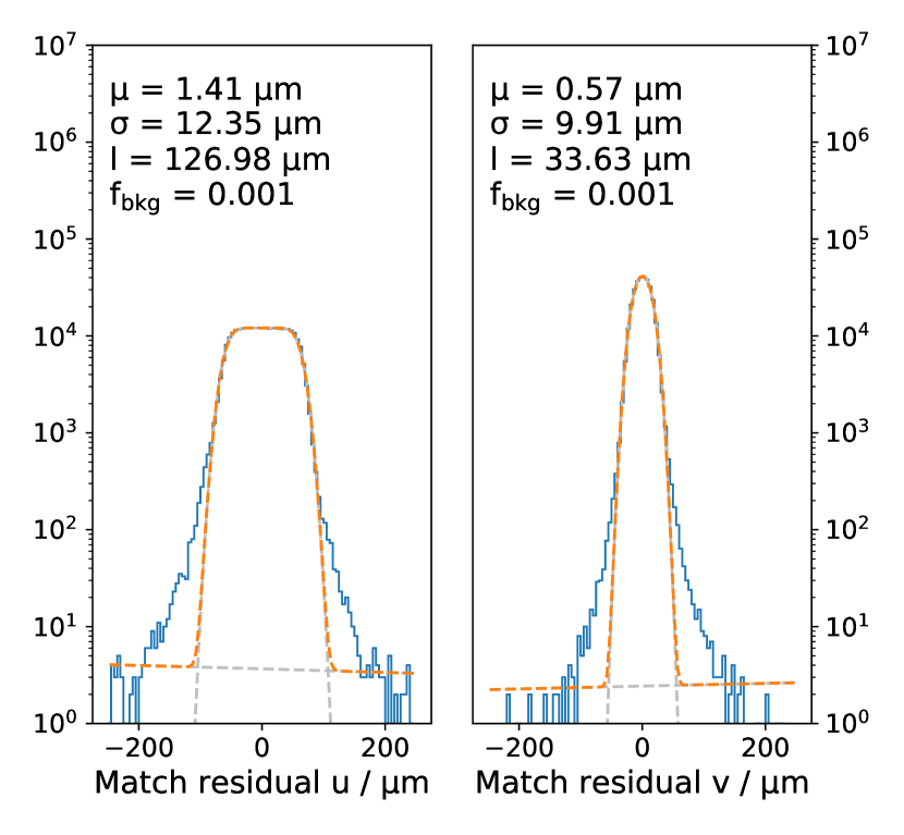
Figure 6 shows the residuals between reconstructed track position and estimated cluster position on the device-under-test for one particular configuration. A matching cut of along both dimensions is used to associate tracks to clusters. The fitted function models the expected response from a pixel of width assuming a telescope resolution of . The vanishing mean along both axis shows that the system is well-aligned. The fitted pixel width along the long u direction is consistent with the pitch. Along the short direction v the fitted width is smaller than the pitch as a result of increased charge sharing. In both cases the background fraction due to mismatches or noise hits is negligible.
Using tracks and clusters within the matching cut, the global efficiency can be calculated as the fraction of tracks with an associated cluster and the total number of tracks. Tracks are only considered within a selected region-of-interest in the central part of the sensors. This avoids edge effects, low statistic regions, and some pixels that were incorrectly tuned. No other cuts or masks are used inside the region-of-interest. The resulting efficiencies as a function of the global threshold are shown in figure 7. The efficiency stays almost constant and with the majority of the measurements above for the selected threshold range. The error bars represent only the statistical uncertainty and do not include systematic effects e.g. known-bad pixels and tuning effects. Additional measurements indicate that the efficiency drops to approximately at a threshold of .
6 Summary
Multiple prototype sensors for the ATLAS ITk upgrade using ams H35 and aH18 CMOS technology have been produced. The H35DEMO is a large scale prototype that can be operated both as a monolithic system with an integrated readout and as a hybrid sensor with a capacitively coupled FE-I4 readout chip. The ATLASPix1 is a first large scale, monolithic prototype designed specifically for the ATLAS ITk upgrade. Both prototypes could be operated in a beam test setup with efficiencies above . This shows that large scale, CMOS pixel sensors in ams technology can be build and operated with a variety of readout options and are a suitable option for the outer layer of the ATLAS ITk upgrade. The ATLASPix1 results only show its basic functionality. Additional performance increases due to better tuning and higher substrate resistivity are expected in the future. Systematic measurements of irradiated ATLASPix1 prototypes with a variety of irradiation sources are currently ongoing to verify previous measurements of radiation hardness with small prototypes [5].
Acknowledgments
The authors gratefully acknowledge the support by the CERN PS and SPS instrumentation team and Fermilab Test Beam Facilities. The authors thank Andreas Nürnberg and Dominik Dannheim for fruitful discussions and collaboration. The research presented in this paper was supported by the SNSF grants 20FL20_173601, 200021_169015 and 200020_169000. This project has received funding from the European Union’s Horizon 2020 research and innovation programme under grant agreement No 675587.
References
- ATLAS Collaboration [2017a] ATLAS Collaboration, Technical Design Report for the ATLAS Inner Tracker Strip Detector, Technical Report CERN-LHCC-2017-005. ATLAS-TDR-025, CERN, Geneva, 2017a.
- ATLAS Collaboration [2017b] ATLAS Collaboration, Technical Design Report for the ATLAS ITk Pixel Detector, Technical Report ATL-COM-ITK-2017-073, CERN, Geneva, 2017b.
- ATLAS Collaboration [2010] ATLAS Collaboration (ATLAS Collaboration), ATLAS Insertable B-Layer Technical Design Report, Technical Report CERN-LHCC-2010-013. ATLAS-TDR-19, CERN, 2010.
- ams AG [2018] ams AG, High Voltage CMOS Processes, 2018. URL: http://ams.com/eng/Products/Full-Service-Foundry/Process-Technology/High-Voltage-CMOS.
- Benoit et al. [2018] M. Benoit, et al., Testbeam results of irradiated ams h18 hv-cmos pixel sensor prototypes, Journal of Instrumentation 13 (2018) P02011.
- Augustin et al. [2015] H. Augustin, et al., The MuPix high voltage monolithic active pixel sensor for the Mu3e experiment, JINST 10 (2015) C03044.
- Augustin et al. [2017] H. Augustin, et al., The MuPix System-on-Chip for the Mu3e Experiment, Nucl. Instrum. Meth. A845 (2017) 194–198. arXiv:1603.08751.
- Vilella et al. [2016] E. Vilella, et al., Prototyping of an hv-cmos demonstrator for the high luminosity-lhc upgrade, Journal of Instrumentation 11 (2016) C01012.
- Cavallaro et al. [2017] E. Cavallaro, et al., Studies of irradiated AMS H35 CMOS detectors for the ATLAS tracker upgrade, JINST 12 (2017) C01074. arXiv:1611.04970.
- Terzo et al. [2017] S. Terzo, et al., Characterisation of novel prototypes of monolithic HV-CMOS pixel detectors for high energy physics experiments, JINST 12 (2017) C06009. arXiv:1705.05146.
- Benoit et al. [2016] M. Benoit, et al., The fe-i4 telescope for particle tracking in testbeam experiments, Journal of Instrumentation 11 (2016) P07003.
- Kiehn et al. [2018] M. Kiehn, et al., Proteus: Pixel telescope reconstruction, https://gitlab.cern.ch/unige-fei4tel/proteus, 2016–2018.
- Benoit et al. [2017] M. Benoit, et al., Test beam measurement of ams H35 HV-CMOS capacitively coupled pixel sensor prototypes with high-resistivity substrate (2017). URL: arXiv:1712.08338. arXiv:1712.08338.