Tailoring Materials for Mottronics:
Excess Oxygen Doping of a Prototypical Mott Insulator
Abstract
The Mott transistor is a paradigm for a new class of electronic devices—often referred to by the term Mottronics—, which are based on charge correlations between the electrons. Since correlation-induced insulating phases of most oxide compounds are usually very robust, new methods have to be developed to push such materials right to the boundary to the metallic phase in order to enable the metal-insulator transition to be switched by electric gating.
Here we demonstrate that thin films of the prototypical Mott insulator LaTiO3 grown by pulsed laser deposition under oxygen atmosphere are readily tuned by excess oxygen doping across the line of the band-filling controlled Mott transition in the electronic phase diagram. The detected insulator to metal transition is characterized by a strong change in resistivity of several orders of magnitude. The use of suitable substrates and capping layers to inhibit oxygen diffusion facilitates full control of the oxygen content and renders the films stable against exposure to ambient conditions, making LaTiO3+x a promising functional material for Mottronics devices.
The rich electronic phase diagram of transition metal oxides caused by strong electron correlations offers new perspectives for future device applications, often referred to as Mottronics. One particularly striking approach is the Mott transistor. In contrast to semiconductor devices, here an electronic phase transition rather than the mere manipulation of charge is employed as a switch. One possible realization is a Mott insulator (OFF-state) that is reversibly driven into a metallic phase (ON-state). Mott insulators as ”failed metals” have metallic charge carrier densities at integer band-filling, but exhibit insulating behavior due to strong on-site Coulomb interactions of the valence electrons. Detuning the band-filling, e.g., by applying an external electric field, can trigger the Mott transition (MT) into the correlated metal phase rendering all previously localized electrons mobile in the ON-state. Besides the large ON/OFF ratio and fast switching speed in such devices, the high charge carrier concentration allows for further miniaturization beyond the current limits set by the extremely small number of carriers in nanoscale semiconductor devices.
The downside of the high charge carrier density, however, is the need for large electric fields to significantly change the band-filling and thereby trigger the phase transition. Such high fields can indeed be achieved by liquid ion gating, which was successfully applied to demonstrate the advanced functionalities of Mott transistors in VO2 and NiNdO3, but may not be suitable for scalable electronics.
Recently, the realization of a Mott transistor involving only moderate electric gate fields was suggested. Dynamical mean field theory (DMFT) based simulations have demonstrated that materials in the Mott insulating phase, but already near the MT, are highly sensitive to external parameters such as strain and temperature, and also electric fields. To reach the operating point close to the transition into the correlated metal phase, the development of methods to tune a material’s position in the electronic phase diagram is crucial. In principle there are two ways to approach the MT, either by decreasing the on-site Coulomb interaction relative to the electron bandwidth (bandwidth controlled MT) or by changing the band-filling (filling controlled MT).
Here, we report on the filling controlled MT in LaTiO3+x (LTO) thin films driven by excess oxygen doping. The material’s tendency to over-oxidize makes the fabrication of LTO thin films challenging, but offers a precise tunability of the band-filling once full control over the oxygen stoichiometry is gained.
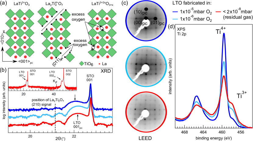
Due to their strong on-site Coulomb interactions and narrow bandwidths 3 perovskites are intensively studied as prototypical Mott systems. The series SrVO3-CaVO3-LaTiO3-YTiO3 exhibits a trend towards increasing electron localization from an enhanced effective electron mass in the metallic vanadates to increasing charge gaps (0.2…1 eV) in the Mott insulating titanates. Recently, it was pointed out that the drastic change of the electronic properties in these seemingly similar materials is based on the progression of an orthorhombic distortion towards the GdFeO3-type structure. In the undistorted cubic perovskite SrVO3 the three bands are degenerate with an effective band-filling of favoring the correlated metal phase. In the distorted titanates, however, the splitting of the levels gives rise to Mott insulating behavior. Stoichiometric LaTiO3 is therefore a prototypical single band Mott insulator and, as indicated by its small Mott gap, already close to the transition into the correlated metal phase.
Further approaching the MT appears possible by -doping with excess oxygen, since LaTiO3 is the endmember of the homologous series LanTinO3n+2. Here, excess oxygen is hosted in the (011)-planes of the pseudocubic (pc) perovskite unit cell with the index denoting the distance between these planes in unit cells ranging from to . The structure of the two endmembers LaTiO3 and La2Ti2O7 with a corresponding configuration of (Ti3+) and (Ti4+) is sketched in Figure 1(a). The existence of these oxygen rich phases poses challenges for the fabrication of stoichiometric LaTiO3 thin films, since the energetically favored valence is Ti4+ and unintentional and uncontrolled over-oxidation may easily occur.
In order to systematically investigate the effects of over-oxidation we fabricated a series of LTO thin films by pulsed laser deposition (PLD) at typical growth parameters on SrTiO3 (STO) substrates in oxygen background pressures of mbar and lower. The structural characterization by x-ray diffraction (XRD) and low-energy electron diffraction (LEED) is depicted in Figure 1(b) and (c) and reveals a general trend: the quality of the diffraction pattern improves for films fabricated in lower oxygen pressure as judged by the Laue intensity oscillations in XRD and the overall contrast and width of the Bragg peaks in LEED. Furthermore, an increase of the lattice constant is detected by XRD for growth in an oxygen pressure of mbar, as indicated by arrows in Figure 1(b). Besides LaTiO3 no other phases are detected. Especially the absence of the La2Ti2O7 signal at 2 and any diffraction peaks from binary titanate compounds as seen in Refs.Ohtomo et al., 2002a and Grisolia et al., 2014 demonstrate the phase purity of the films. Note that the 2x2 surface reconstruction with respect to the pc unit cell in LEED is in line with the GdFeO3-type perovskite structure.
The effect of doping is studied by monitoring the valence of the titanium cations as probed by x-ray photoelectron spectroscopy (XPS) of the Ti 2 core level. Due to the screening by the additional 3 electron the binding energy of the Ti 2 core level of Ti3+-ions is reduced with respect to that of Ti4+-ions, making this core level an excellent measure of the 3 band-filling. The measurements were carried out in situ, i.e., keeping the samples in ultra high vacuum after PLD growth, to avoid any post-fabrication oxidation. As is clear from Figure 1(d), all samples suffer from strong over-oxidation. Even for fabrication in vacuum ( mbar) the dominating valency is Ti4+, corresponding to an electronic occupancy far away from half band-filling. Similar to the La2Ti2O7 phase, breaking the shared corners of adjacent TiO6 octahedra allows the incorporation of excess oxygen ions but—in contrast to La2Ti2O7—only locally and in a random manner as sketched for the LaTiO3+x case in Figure 1(a). Such randomly distributed excess oxygen does not result in coherent Bragg peaks, making diffraction techniques insensitive to this kind of over-oxidation. Therefore a direct characterization of the electronic properties is crucial and an analysis of the merely structural properties may be misleading.
At this point, we briefly comment on the implications of these results for oxide heterostructures, in which LTO is frequently integrated as an electron donor layer. In such structures special care about the titanium valency should be exercised, since the observation of Ti4+ in the LTO layer may not prove the intended electron transfer. It rather could signal the over-oxidation discussed above.
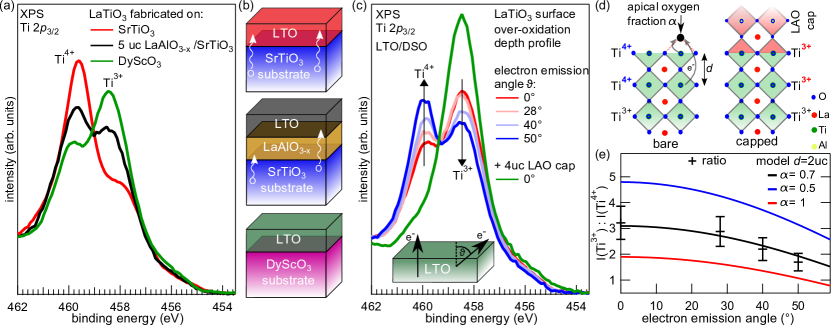
Avoiding over-oxidation, i.e., gaining control of the oxygen stoichiometry in LTO thin films is an essential prerequisite for controlled -doping. Due to the elevated temperatures required during thin film fabrication substantial oxygen diffusion between substrate and film is expected. Since STO is prone to oxygen vacancy formation upon vacuum annealing and exhibits a high oxygen diffusion coefficient, we expect a strong oxygen out-diffusion from this substrate material. This hypothesis is tested by introducing an epitaxial LaAlO3-x (LAO) buffer layer between substrate and LTO film to block the oxygen out-diffusion. As depicted in Figure 2(a), these samples indeed exhibit an increased Ti3+ signal (black curve) but still show a dominant Ti4+ contribution. The latter can be further reduced by employing DyScO3 (DSO) substrates such that the Ti3+ signal is prevailing. Upon reducing the Ti4+ content, the structural properties as characterized by RHEED and LEED further improve. A layer-by-layer growth mode and an atomically flat and clean LTO surface is achieved for fabrication on DSO substrates as discussed in detail in Section S1 (Supporting Information). Note that for epitaxy on DSO substrates the best structural properties and lowest Ti4+ content are achieved for growth in an oxygen background pressure of mbar, and not in vacuum as for STO based samples (see Figure S2, Supporting Information). Without a sizable oxygen out-diffusion from the DSO substrate, additional oxygen needs to be supplied to reach the optimal oxidation conditions for the growth of LTO thin films.
The origin of the remaining over-oxidation on DSO based samples is of a different nature, as revealed by angle-dependent XPS measurements presented in Figure 2(c). Increasing the photoelectron emission angle towards grazing emission—and thereby decreasing the effective probing depth —results in a strong enhancement of the Ti4+ signal. This demonstrates that the remaining over-oxidation is limited to a strongly confined surface layer on the length scale of the photoelectron inelastic mean free path . A plausible origin for this surface over-oxidation is the adsorption of additional oxygen ions at the apical sites completing the surface TiO6 octahedra and removing two electrons per anion from the LTO film, as sketched in Figure 2(d). Such apical oxygen ligands have already been detected by scanning tunneling microscopy on the surface of the related perovskite SrVO3. A quantitative evaluation of the Ti3+ to Ti4+ intensity ratio supports this scenario and is plotted in Figure 2(e). Due to an apical oxygen coverage , a surface layer containing Ti4+-ions with an extension of unit cells is assumed. The angle-dependent XPS data is best reproduced for uc and a coverage 75%. Details of the model calculation can be found in Section S3 (Supporting Information).
These apical oxygen sites can be blocked by an epitaxial LAO capping layer. Since the cations in the LAO capping layer are of the same oxidation states as the cations in bulk LTO, the situation for the topmost TiO2 layer (the former surface layer) is similar to bulk LTO. The oxygen octahedra are completed and the lanthanum and aluminum cations of the capping layer supply their share of electrons, thereby avoiding an electron depletion from Ti3+-ions (see Figure 2(d)). LAO-capped LTO thin films grown on DSO substrates indeed exhibit no Ti4+ signal indicating a stoichiometric LaTi3+O3 thin film (see green spectrum in Figure 2(c)). Furthermore the capping layer prevents any further oxidation upon exposure to air which is crucial for future device fabrication (see Section S4, Supporting Information).
We like to point out here that the complex over-oxidation mechanisms in LTO thin films have recently led to confusion about the line shape of the 2 spectrum in transition metal oxides. It has been argued that photoemission final states always lead to a Ti4+ signal even for stoichiometric LTO exclusively comprised of Ti3+-ions. Our measurements, however, give proof that this is not the case. Rather, a pure Ti3+ spectrum without any detectable additional satellite structures is observed. For reference the Ti 2 photoemission and the Ti edge x-ray absorption spectra of stoichiometric LTO thin films are provided in Figure S5 (Supporting Information).
Having demonstrated how to gain control of the oxygen stoichiometry, we now deliberately tune the over-oxidation to drive the filling controlled MT.
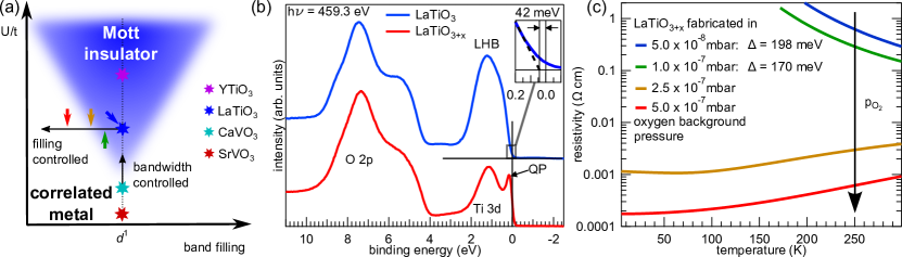
The electronic phase diagram as function of correlation strength vs. band-filling is schematically depicted in Figure 3(a), where is the on-site Coulomb repulsion and the intersite hopping integral. For orientation also the series of prototypical -materials discussed above is included. The different members (colored stars) are situated on different positions along the bandwidth controlled MT, which is depicted by the vertical arrow. Reducing the band-filling by supplying excess oxygen allows us to continuously change the position along the filling controlled MT, marked by the horizontal arrow and starting from stoichiometric LTO (blue star) in Figure 3(a). As shown above, additional oxygen can easily be incorporated in LTO thin films by increasing the oxygen pressure applied during thin film fabrication. Every excess oxygen ion removes two electrons from the titanium 3 band, which eventually leads to a transition into the correlated metal phase.
We employ resonant photoemission at the Ti absorption edge to monitor the Ti 3 spectral function across the transition. Note that the samples were measured in situ and without an LAO capping. The photoelectron inelastic mean free path in this experiment is high enough to probe the bulk LTO film below the over-oxidized surface layer. For the employed photon energy of eV, and the relative contribution of the bulk signal is about 50. Furthermore, the resonant conditions strongly and selectively enhance the Ti 3 photoemission signal. The resulting spectra of a stoichiometric and a -doped LTO thin film are depicted in Figure 3(b). In the stoichiometric case a single Ti 3 feature is observed near the chemical potential and identified as the lower Hubbard band (LHB) characteristic for the Mott insulating phase. Interestingly, the over-oxidized surface layer on these bare LTO samples does not lead to metallic charge carriers, signalled by the absence of a Fermi cutoff. The most plausible scenario is that the surface layer rather forms areas with a band-filling of , i.e., with no contribution to the Ti 3 spectrum, and subjacent or adjacent stoichiometric areas in the Mott insulating phase with a band-filling. Thus, no trace of intermediately doped (i.e. metallic) areas is detected. The onset of the LHB is found at a binding energy of meV, which is a lower limit for the Mott gap between the upper and the lower Hubbard band. The presence of a lower Hubbard band and a gap size of at least meV indicate that the Ti 3 electrons are fully localized.
For the -doped sample, labeled LaTiO3+x in Figure 3(b), a Fermi cutoff and the typical two peak structure of a correlated metal, consisting of a coherent quasi-particle peak (QP) and an incoherent LHB, is observed. These findings demonstrate that fabrication of LTO thin films at elevated oxygen pressure is a suitable method to reduce the band-filling and trigger the MT.
To directly probe the transport properties, which are crucial for device applications, we have also performed complementary temperature dependent resistivity measurements. As depicted in Figure 3(c), an activated behavior is observed for stoichiometric samples fabricated in an oxygen pressure of mbar. An Arrhenius-type temperature dependence of the resistivity with reproduces the data and yields a Mott gap of meV. Upon -doping by means of increasing the oxygen growth pressure, the gap initially decreases to meV for growth in mbar of oxygen before it collapses for higher oxygen pressures as indicated by the metal-like temperature dependence. The change of resistivity is drastic as the phase boundary is crossed, being a factor of approx. 100 at room temperature and even several orders of magnitude higher at low temperatures. The resulting positions of these samples in the electronic phase diagram are marked by arrows in the corresponding colors in Figure 3(a).
The characteristics of the MT described above make the material an exciting candidate for Mott transistors. Samples on the insulating side of the phase transition exhibit a Mott gap of about meV, large enough to avoid thermally activated transport crucial for a well defined OFF-state. The phase transition is easily reached by -doping and yields a change of orders of magnitude in conductivity. In addition, the material’s position relative to the band-filling induced MT can be adjusted by an easily controlled fabrication parameter, i.e., the oxygen pressure.
Besides the band-filling control demonstrated above, fabrication of LTO as thin films allows for further tuning of the electronic properties. For instance, the bandwidth can be effectively reduced by decreasing the film thickness in favor of the Mott insulating phase. Strain engineering and thereby manipulating the in-plane lattice parameter is another approach and works both ways—increasing and decreasing allows to shift the material towards the correlated metal and Mott insulating phase, respectively.
The possibility to relocate the material’s position in the electronic phase diagram is especially important for the optimization of the operating point of future Mott transistor devices. As discussed above, approaching the phase transition from the insulating side is predicted to make the material susceptible to moderate electric fields, thereby allowing for conventional field effect setups.
Turning from the high controllability of the electronic properties in LTO thin films to the practical realization of a field effect based Mott transistor, the material’s perovskite crystal structure is advantageous. This material class offers many epitaxially compatible functional compounds, ready for the design of all-oxide devices. For instance the two main components of a field effect device, dielectric and electrode, can be realized by the high- material STO and highly conductive SrRuO3 or SrVO3, respectively.
In summary, we have established a suitable method to control the band-filling in the prototypical Mott insulator LTO by excess oxygen doping. The films can readily accommodate excess oxygen ions, which was demonstrated as an effective way of -doping to control the material’s electronic properties. The choice of the substrate was found to be crucial to gain control of the oxygen stoichiometry. Films grown on STO are inherently over-oxidized, while fully stoichiometric LTO thin films were fabricated on DSO substrates. These are important steps in material development towards the realization of a Mott transistor, which elegantly utilizes the concept of conventional field effect setups, while harnessing at the same time the peculiar electronic properties caused by electron correlations.
Experimental Section
Substrate termination: A TiO2 surface termination of STO (001) substrates was achieved by rinsing in deionized water, etching with
hydrofluoric acid, and subsequent annealing in oxygen as described elsewhere. ScO2-terminated surfaces of DSO (110) (orthorhomic notation) were prepared by annealing in oxygen, followed by etching in NaOH. All substrates were supplied by CrysTec GmbH.
LaTiO3 thin film epitaxy by pulsed laser deposition (PLD): A PLD system with a base pressure in the 10mbar range was used to fabricate the LTO thin films. To stabilize oxygen pressures in the 10mbar range at elevated temperatures, a UHV anneal of the substrates at 500C was performed prior to the ablation process. The substrate temperature during ablation was held at C. Temperature control was realized by an infrared laser (nm) and a two color pyrometer, both directed to the back side of the sample holder. The LTO material was ablated from a polycrystalline LaTiO3+x target by a KrF excimer laser (nm) with a laser fluency of J/cm2 at a repetition rate of Hz and a target-to-substrate distance of mm. The resulting growth rate was 30 pulses per unit cell, as monitored by RHEED intensity oscillations. The thickness of the fabricated LTO thin films was between 20 and 40 uc. For samples fabricated in oxygen background pressure, the oxygen dosing valve was closed directly after the ablation process and the samples were cooled down to room temperature in vacuum. The LAO capping layers were ablated from a single crystalline LaAlO3 target with J/cm2 and Hz in an oxygen background atmosphere of mbar. During epitaxy of the capping the substrate was held at C.
LTO thin film characterization: The PLD chamber is attached to a UHV cluster with a base pressure in the mbar range, allowing for an in situ characterization by XPS and LEED directly after the PLD growth. The XPS setup utilizes a monochromatized Al Kα x-ray source and an Omicron EA-125 electron analyzer with an overall energy resolution of approx. 0.40 eV. Resonant photoemission measurements were performed at the two-color beamline I09 at DIAMOND Light source using linearly polarized light with a photon energy of 459.3 eV. Hard x-ray photoemission was performed on the same spot (size 30m x 50m) with a photon energy of 3 keV. The spectra were recorded with an EW4000 photoelectron analyzer (VG Scienta, Uppsala, Sweden) equipped with a wide-angle acceptance lens. A portable UHV chamber with a base pressure in the 10mbar range equipped with a NEG pump was used to ship the samples to DIAMOND light source and prevent oxidation during transport. Temperature dependent resistivity measurements were performed in the Van-der-Pauw geometry using a Quantum Design Physical Properties Measurement System (PPMS) on LTO thin films capped with 5 uc LAO to prevent oxidation in air. Electrical contacts on the LTO thin films were realized by ultrasonic wire bonding with Al wires.
Supporting Infromation
Supporting Information is available online or from the authors.
Acknowledgements
The authors are grateful for funding support from the Deutsche Forschungsgemeinschaft (FOR 1162 and SFB 1170 ”ToCoTronics”) and acknowledge Diamond Light Source for time on beamline I09 under proposal SI14106, SI15200, SI15856, and NT18372. The authors would also like to thank D. McCue for his superb technical support at the I09 beamline. We also acknowledge fruitful discussion with M. Bibes and R. Aeschlimann.
References
- Takagi and Hwang (2010) H. Takagi and H. Y. Hwang, Science 327, 1601 (2010).
- Ahn et al. (2003) C. H. Ahn, J.-M. Triscone, and J. Mannhart, Nature 424, 1015 (2003).
- Son et al. (2011) J. Son, S. Rajan, S. Stemmer, and S. J. Allen, J. Appl. Phys. 110, 084503 (2011).
- Nakano et al. (2012) M. Nakano, K. Shibuya, D. Okuyama, T. Hatano, S. Ono, M. Kawasaki, Y. Iwasa, and Y. Tokura, Nature 487, 459 (2012).
- Inoue and Rozenberg (2008) I. H. Inoue and M. J. Rozenberg, Advanced Functional Materials 18, 2289 (2008).
- Mazza et al. (2016) G. Mazza, A. Amaricci, M. Capone, and M. Fabrizio, Physical Review Letters 117, 176401 (2016).
- Newns et al. (1998) D. M. Newns, J. A. Misewich, C. C. Tsuei, A. Gupta, B. A. Scott, and A. Schrott, Applied Physics Letters 73, 780 (1998).
- Imada et al. (1998) M. Imada, A. Fujimori, and Y. Tokura, Reviews of Modern Physics 70, 1039 (1998).
- Inoue (2005) I. H. Inoue, Semicond. Sci. Technol. 20, 112 (2005).
- Castell et al. (2003) M. R. Castell, D. A. Muller, and P. M. Voyles, Nature Materials 2, 129 (2003).
- Chudnovskiy et al. (2002) F. Chudnovskiy, S. Luryi, and B. Spivak, Future Trends in Microelectronics: The Nano Millenium, edited by S. Luryi, J. M. Xu, and A. Zaslavsky (Wiley, Hoboken, New Jersey, 2002) p. 148.
- Scherwitzl et al. (2010) R. Scherwitzl, P. Zubko, I. G. Lezama, S. Ono, A. F. Morpurgo, G. Catalan, and J.-M. Triscone, Advanced Materials 22, 5517 (2010).
- Zhong et al. (2015) Z. Zhong, M. Wallerberger, J. M. Tomczak, C. Taranto, N. Parragh, A. Toschi, G. Sangiovanni, and K. Held, Physical Review Letters 114, 246401 (2015).
- Fujimori et al. (1992) A. Fujimori, I. Hase, H. Namatame, Y. Fujishima, Y. Tokura, H. Eisaki, S. Uchida, K. Takegahara, and F. M. F. de Groot, Physical Review Letters 69, 1796 (1992).
- Arima et al. (1993) T. Arima, Y. Tokura, and J. B. Torrance, Physical Review B 48, 17006 (1993).
- Haverkort et al. (2005) M. W. Haverkort, Z. Hu, A. Tanaka, G. Ghiringhelli, H. Roth, M. Cwik, T. Lorenz, C. Schüßler-Langeheine, S. V. Streltsov, A. S. Mylnikova, V. I. Anisimov, C. de Nadai, N. B. Brookes, H. H. Hsieh, H.-J. Lin, C. T. Chen, T. Mizokawa, Y. Taguchi, Y. Tokura, D. I. Khomskii, and L. H. Tjeng, Physical Review Letters 94, 056401 (2005).
- Pavarini et al. (2004) E. Pavarini, S. Biermann, A. Poteryaev, A. I. Lichtenstein, A. Georges, and O. K. Andersen, Physical Review Letters 92, 176403 (2004).
- Lichtenberg et al. (2001) F. Lichtenberg, A. Herrnberger, K. Wiedenmann, and J. Mannhart, Progress in Solid State Chemistry 29, 1 (2001).
- Ohtomo et al. (2002a) A. Ohtomo, D. A. Muller, J. L. Grazul, and H. Y. Hwang, Applied Physics Letters 80, 3922 (2002a).
- Disa et al. (2015) A. S. Disa, D. P. Kumah, A. Malashevich, H. Chen, D. A. Arena, E. D. Specht, S. Ismail-Beigi, F. J. Walker, and C. H. Ahn, Physical Review Letters 114, 026801 (2015).
- Ohtomo et al. (2002b) A. Ohtomo, D. A. Muller, J. L. Grazul, and H. Y. Hwang, Nature 419, 378 (2002b).
- Biscaras et al. (2012) J. Biscaras, N. Bergeal, S. Hurand, C. Grossetête, A. Rastogi, R. C. Budhani, D. LeBoeuf, C. Proust, and J. Lesueur, Physical Review Letters 108, 247004 (2012).
- Wong et al. (2010) F. J. Wong, S.-H. Baek, R. V. Chopdekar, V. V. Mehta, H.-W. Jang, C.-B. Eom, and Y. Suzuki, Physical Review B 81, 161101 (2010).
- Takizawa et al. (2006) M. Takizawa, H. Wadati, K. Tanaka, M. Hashimoto, T. Yoshida, A. Fujimori, A. Chikamatsu, H. Kumigashira, M. Oshima, K. Shibuya, T. Mihara, T. Ohnishi, M. Lippmaa, M. Kawasaki, H. Koinuma, S. Okamoto, and A. J. Millis, Physical Review Letters 97, 057601 (2006).
- Chang et al. (2013) Y. J. Chang, L. Moreschini, A. Bostwick, G. A. Gaines, Y. S. Kim, A. L. Walter, B. Freelon, A. Tebano, K. Horn, and E. Rotenberg, Physical Review Letters 111, 126401 (2013).
- Lin et al. (2015) C. Lin, A. Posadas, T. Hadamek, and A. A. Demkov, Physical Review B 92, 035110 (2015).
- Grisolia et al. (2014) M. N. Grisolia, F. Y. Bruno, D. Sando, H. J. Zhao, E. Jacquet, X. M. Chen, L. Bellaiche, A. Barthélémy, and M. Bibes, Applied Physics Letters 105, 172402 (2014).
- Cao et al. (2016) Y. Cao, X. Liu, M. Kareev, D. Choudhury, S. Middey, D. Meyers, J.-W. Kim, P. J. Ryan, J. W. Freeland, and J. Chakhalian, Nature Communications 7, 10418 (2016).
- Schneider et al. (2010) C. W. Schneider, M. Esposito, I. Marozau, K. Conder, M. Doebeli, Y. Hu, M. Mallepell, A. Wokaun, and T. Lippert, Applied Physics Letters 97, 192107 (2010).
- Dudy et al. (2016) L. Dudy, M. Sing, P. Scheiderer, J. D. Denlinger, P. Schütz, J. Gabel, M. Buchwald, C. Schlueter, T.-L. Lee, and R. Claessen, Advanced Materials 28, 7443 (2016).
- Paladino et al. (1965) A. E. Paladino, L. G. Rubin, and J. S. Waugh, Journal of Physics and Chemistry of Solids 26, 391 (1965).
- Henrich et al. (1978) V. E. Henrich, G. Dresselhaus, and H. J. Zeiger, Physical Review B 17, 4908 (1978).
- Posadas et al. (2017) A. B. Posadas, K. J. Kormondy, W. Guo, P. Ponath, J. Geler-Kremer, T. Hadamek, and A. A. Demkov, J. Appl. Phys. 121, 105302 (2017).
- Sing et al. (2009) M. Sing, G. Berner, K. Goß, A. Müller, A. Ruff, A. Wetscherek, S. Thiel, J. Mannhart, S. A. Pauli, C. W. Schneider, P. R. Willmott, M. Gorgoi, F. Schäfers, and R. Claessen, Physical Review Letters 102, 176805 (2009).
- Okada et al. (2017) Y. Okada, S.-Y. Shiau, T.-R. Chang, G. Chang, M. Kobayashi, R. Shimizu, H.-T. Jeng, S. Shiraki, H. Kumigashira, A. Bansil, H. Lin, and T. Hitosugi, Physical Review Letters 119, 086801 (2017).
- Yoshimatsu et al. (2010) K. Yoshimatsu, T. Okabe, H. Kumigashira, S. Okamoto, S. Aizaki, A. Fujimori, and M. Oshima, Physical Review Letters 104 (2010), 10.1103/PhysRevLett.104.147601.
- Yoshimatsu et al. (2016) K. Yoshimatsu, H. Okabe, T. Oshima, S. Ueda, and A. Ohtomo, Physical Review B 93, 195159 (2016).
- Okhay et al. (2013) O. Okhay, A. Tkach, A. Wu, and P. M. Vilarinho, Journal of Physics D: Applied Physics 46, 505315 (2013).
- Moyer et al. (2013) J. A. Moyer, C. Eaton, and R. Engel-Herbert, Advanced Materials 25, 3578 (2013).
- Koster et al. (1998) G. Koster, B. L. Kropman, G. J. H. M. Rijnders, D. H. A. Blank, and H. Rogalla, Applied Physics Letters 73, 2920 (1998).
- Kleibeuker et al. (2012) J. E. Kleibeuker, B. Kuiper, S. Harkema, D. H. A. Blank, G. Koster, G. Rijnders, P. Tinnemans, E. Vlieg, P. B. Rossen, W. Siemons, G. Portale, J. Ravichandran, J. M. Szepieniec, and R. Ramesh, Physical Review B 85, 165413 (2012).