Doped and Codoped Silicon Nanocrystals: the Role of Surfaces and Interfaces
Abstract
Si nanocrystals have been extensively studied because of their novel properties and their potential applications in electronic, optoelectronic, photovoltaic, thermoelectric and biological devices. These new properties are achieved through the combination of the quantum confinement of carriers and the strong influence of surface chemistry. As in the case of bulk Si the tuning of the electronic, optical and transport properties is related to the possibility of doping, in a controlled way, the nanocrystals. This is a big challenge since several studies have revealed that doping in Si nanocrystals differs from the one of the bulk. Theory and experiments have underlined that doping and codoping are influenced by a large number of parameters such as size, shape, passivation and chemical environment of the silicon nanocrystals. However, the connection between these parameters and dopant localization as well as the occurrence of self-purification effects are still not clear. In this review we summarize the latest progress in this fascinating research field considering free-standing and matrix-embedded Si nanocrystals both from the theoretical and experimental point of view, with special attention given to the results obtained by ab-initio calculations and to size-, surface- and interface-induced effects.
keywords:
Semiconducting nanocrystals, quantum confinement effects, doping, surface physics1 Introduction
Silicon has become the most studied material in the past decades owing to its unique characteristics: Si is the second most abundant element (after oxygen) in the Earth’s crust, making up 25.7% of its mass; it can be produced with impurity levels of less than ; it remains a semiconductor at higher temperatures than germanium; its native oxide is easily grown in a furnace and forms a better semiconductor/insulator interface than any other material. Silicon is not only easy to handle and fairly simple to manufacture but it is also cheap. Moreover it shows excellent electrical properties, high stability, optimal thermal characteristics and high mechanical strength. For these motives, this environmental friendly material is the most used element in semiconductor industry and, today, it represents the electronic material per excellence. It is also commonly used for solar or photovoltaic applications and its role in the optoelectronic industry is becoming more and more important.
However, the rapid evolution in the electronic, optoelectronic and photovoltaic sectors is facing severe constrictions due to the actual physical limits of Si-based technologies[1, 2, 3]. Some examples are: i) the limitations in the operating speed of microelectronic devices due to interconnects, ii) bulk Si is an indirect band-gap material which emits in the infrared region with very low efficiency, iii) radiative recombination times in Si are very large, so the de-excitation dynamics are strongly affected by the occurrence of fast non-radiative recombinations mechanisms, iv) bulk Si shows a significant free carrier absorption and Auger recombination rates which impede population inversion and, hence, optical gain, v) its band gap impedes fully exploitation of solar radiation in photovoltaic applications, vi) the absence of a bulk second-order dipolar nonlinear optical susceptibility due to the bulk crystal centrosymmetry, that do not permit to use bulk Si in order to produce a wide variety of wavelengths from an optical pump.
The increasing demand for new, innovative and more efficient devices has driven scientists to explore new functionalities in Si-based materials. In photonics the main interest lies in the possibility to merge electronics and photonics on the same chip and therefore to render Si a good light emitter. Moreover the introduction of second-order nonlinearity by proper material engineering would be highly desirable, because the all-optical data management requires nonlinear silicon photonics [4]. Finally, for photovoltaic applications we have to add to Si new features in order to maximize solar radiation harvesting and to minimize loss by thermalization processes.
The advent of nanoscience and nanotechnologies and the consequent scaling down of Si structures to nanometer sizes have opened new possibilities to overcome the inability of bulk-Si as efficient light emitter. Moreover, the capacity of altering energy gap and optoelectronic properties by size reduction, and therefore to enhance solar light harvesting, has opened new possibilities in the development of new efficient, nanostructured, Si-based solar cell devices.
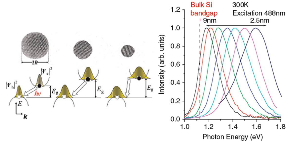
It has been suggested that the problems related to the indirect band-gap of bulk-Si might be overcome in highly confined systems. For example, in low-dimensional Si-based nanostructures such as porous-Si, a quantum sponge made up of Si nanostructures, nanowires (Si-NWs) and nanocrystals (Si-NCs), the possibility to achieve efficient visible photoluminescence (PL) has been demonstrated [5, 6, 7, 8]. In these nanostructures the low-dimensionality causes the zone folding of the conduction band minimum of bulk Si, that is located near the -point, thus introducing a quasi-direct band gap. Moreover the quantum confinement (QC) effect associated with the reduced size of the nanosystems enlarges the energy band gap enabling light emission in the visible range [9]. This effect can also enhance the spatial localization of electron (e) and hole (h) wave functions and their overlap, and therefore the probability of e-h recombination (see Fig. 1).
.
Among the different Si-based nanostructures, Si-NCs have attracted, from the beginning, much interest because they exhibit very bright visible PL (see Fig. 1), which is tunable with respect to the dimension of the Si-NCs [10], and sample dependent high quantum yields, ranging from 1 up to 60. The quantum yields can be enhanced by careful surface passivation and by avoiding oxygen contamination during all stages of the Si-NC preparation [11]. Moreover optical gain in Si-NCs has been successfully observed and discussed [12, 13, 14, 15, 16, 17, 18, 19] as well as giant Raman gain [20, 21]. Finally carrier multiplication effects in excited carrier dynamics after the absorption of a single high-energy photon have been observed in ensemble of Si-NCs, proving thus the possibility of better exploiting processes of photo-generated carriers to increase solar cell performances [22, 23, 24, 25, 26, 27, 28, 29].
The possibility to exploit the size, shape and surface termination [30] of the Si-NCs togheter with their low toxicity and good biocompatibility has prompted their application in several broad fields such as microeletronics [2, 31, 32], photonics [33, 34], non-linear optics [35, 36, 37], secure communications [36], photovoltaics, in the so-called third-generation solar cells, solar fuels [3, 38, 39, 40, 41, 42, 43], thermoelectrics [44, 45] and biomedicine [46, 47, 48, 49, 50].
Visible PL in Si nanostructures has been attributed to transition between states localized inside the Si-NC [51, 52, 53, 54], or between defects and/or interface states [55, 56, 57, 58, 59, 60]. Despite the discussion on which of the above mechanisms primarily determines the emission energy is still open, recent results seem to indicate the coexistence of both the effects, whose relevance depends on the structural properties of the sample [55, 56, 61, 62, 63, 64, 65, 66, 67, 68, 69, 70, 71]. In particular, it was suggested that for diameters above a certain threshold (from about 3 nm up to diameters of the order of two times the bulk Si exciton Bohr radius, about 9 nm) the emission peak of the Si-NCs simply follows the QC model, while interface states assume a crucial role only for small-sized Si-NCs (less than 3 nm) [69, 72, 73, 74].
It is well known that an additional degree of freedom in semiconductor materials design is given by the introduction of impurities. Controlled doping is at the heart of the modern Si-based semiconductor industry. The best known example is the p-n junction. Here elements of the column III and V, like the B and P atoms, are used to electrically dope the Si by introducing positive holes or negative electrons. The presence of the doping atoms changes remarkably the optical and electronic properties of the hosting material. B and P impurities introduce very shallow levels in the band gap of bulk Si, above the valence band and below the conduction band, than can be efficently ionized at room temperature increasing dramatically the conductivity of bulk Si.
Doping in Si-NCs, as in bulk semiconductor devices, can be used to alter in a controllable way the electronic, optical and transport properties of nanomaterials. As a consequence, intentional doping with n- and p-type impurities can be exploited to design and realize novel devices based on Si-NCs.
The possibility of enhancing the electrical conductivity of nanosized systems has been attempted, for instance, by obtaining porous Si from n- or p-doped bulk Si by means of an electrochemical etching [75]. Nevertheless, even for the larger mesoporous samples, a very low conductivity was measured, despite the fact that the etching process does not remove the impurities from the system [76]. This suggests that the ionization of the impurities at room temperature may be strongly quenched with respect to the bulk. Therefore the possibility of generating free charge carriers from impurity states can be limited by size effects.
Regarding the optical properties, the introduction in the Si-NC of an isoelectronic impurity can circumvent the indirect gap behavior of bulk Si. However Si does not possess proper isoelectronic impurities that can strongly localize excitons at room temperature and enhance the PL intensity. An alternative approach is given by codoping. i.e. the formation of Si nanocrystals with the same number of n- and p-type impurities [77]. The first attempts to dope Si-NCs started about 20 years ago. The results obtained revealed that doped Si-NCs showed different properties with respect to the doped Si-bulk [78, 79].
For example a shallow impurity level in bulk may become a deep level at the nanoscale. In bulk Si the level of doping lies in the interval 1013-1018 cm-3. In a Si-NC of about 2 nm in diameter, which possess more than 200 Si atoms, the introduction of a single impurity atom corresponds to a doping level of about 1020 cm-3, that is a quite different situation. Despite the large number of works dedicated to the study of doped and codoped Si-NCs, important issues still exist. The effective dopant location (within the nanocrystals, at their surface-interface, or in the surrounding matrix?), the occurrence of self-purifications effects (that is the tendency of the Si-NC to expel the dopant atoms to its surface) as well as the role played by the chemical environmental of the Si-NC are issues not yet solved by the scientific community [76, 78, 79, 80, 81, 82, 83, 84, 85, 86, 87].
Experimentally, several factors contribute to make the interpretation of the measurements on these systems a difficult task. First of all, independently on the fabrication technique, in experimental samples there aren’t two identical Si-NCs. For instance, samples show a strong dispersion in the Si-NC size, that is difficult to determine. In this case it is possible that the observed quantity does not correspond exactly to the mean size but instead to the most responsive Si-NCs [88]. Moreover, Si-NCs synthesized by different techniques often show different properties in size, shape and in the interface structure. Finally, in solid nanocrystal arrays some collective effects caused by electron, photon, and phonon transfer between Si-NCs can render more complicated the interpretation of the experimental results.
The aim of this review is to summarize the latest progress in the fascinating research field related to the understanding of the doping in Si-NCs with n- and p-type impurities. It should be pointed out that in these last few years some review articles on this topic have been published[41, 78, 79, 89, 90]. At variance with these reviews, since the role of theoretical modelings and simulations has becomed more an more important, we will give particular attention to the theoretical outcomes. Moreover we will focus our attention not only on single doped Si-NCs but also on compensated codoped Si-NCs, a very interesting and rapidly growing field. Mainly, we will consider B and P as dopant atoms due to their high solid solubility in silicon and because they are the most commonly used impurities in experiments.
In this work we will use the notation ”doped Si-NCs” to indicate systems where B and/or P atoms are incorporated in Si-NCs. However, in principle, it would be better to speak about impurity atoms in the case of simple incorporation and of dopants in the case of activated impurities. Nevertheless in line with the use in the literature we will adopt the term dopant; it will be clear from the discussion the real meaning of this term.
The review is organized as follows. First, in section 2 we will sketch the ab-initio models used for the calculations of the structural, electronic and optical properties of the nanostructures. In section 3 we will review the experimental results regarding doped free-standing Si-NCs, with particular focus on the theoretical outcomes (see subsections 3.1 and 3.2). Section 4 is instead devoted to the discussion of the properties of matrix-embedded doped Si-NCs; a subsection is dedicated to the theoretical results (subsection 4.1). Transport is discussed in section 5, whereas section 6 is entirely devoted to the study of codoped compensated Si-NCs. Conclusions are presented in section 7.
2 Theoretical Modelling
.
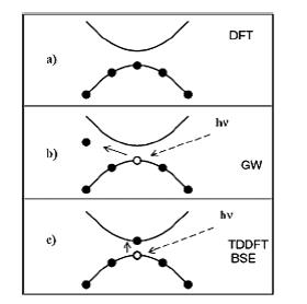
The structural, electronic and optical properties of complex systems are nowadays accessible, thanks to the impressive development of theoretical approaches and to the availability of High-Performance Computing platforms. Surfaces, nanostructures, and even biological systems can now be studied within ab-initio methods [19, 87]. In principle, within the Born-Oppenheimer approximation to decouple the ionic and electronic dynamic, the equation that governs systems of strongly interacting particles is the Many-Body (MB) equation whose solution is a formidable task. Among all, the single-particle Density Functional Theory (DFT) is one of the most popular methods to study ground state properties of systems of interacting particles. This approach allows to map an interacting quantum MB system into a fictitious system of non-interacting particles. The Green function approach, instead, permits to calculate the excitations of a system of interacting particles by mapping the MB electronic problem into a problem of weakly interacting quasi-particles, where the quasi-particle describes the particle plus its screened interaction with the rest of the system. Fig. 2 shows some schemes used to calculate ground state properties, band structures, and optical spectra: DFT for ground state properties, GW for band structure calculations (charged excitations), and the Bethe-Salpeter equation (BSE) and the time dependent (TD) DFT approaches for optical spectra (neutral excitations).
Concerning DFT, it is worth noting that the Kohn-Sham (KS) equations, on which the method is based, represent a fictitious auxiliary system with no physical meaning. Nevertheless, their eigenvalues are often interpreted as one-electron excitation energies corresponding to the excitation spectra of the system upon removal or addition of an electron, and DFT is in this way used to calculate band structures. The qualitative agreement with experiments is often remarkable. The quantitative agreement, instead, depends on the approximations used to describe the exchange-correlation energy in the KS equations. The most used approximations, named local density approximation (LDA) and generalised gradient approximation (GGA), lead to a systematic underestimation of the semiconductor energy gap. This fact can be overcomed by computing quasiparticle energies within the GW scheme. This approach represents the most refined method for the band structure calculation of solids, surfaces, nanostructures and for the determination of the energy levels of molecules and atoms. GW well describes direct and inverse photoemission spectroscopies (see panel b of Fig. 2), where the final state is a charged system since one electron have been removed or add to the system, but fails to describe optical excitations. A correct description of optical spectra (see panel c of Fig. 2) for both free-standing and embedded Si-NCs requires an appropriate treatment of the local field effects [72, 73] and an exhaustive calculation of the electron-hole interaction, that can be obtained by solving the BSE within the Many-Body Perturbation Theory (MBPT) [91].
In the DFT+MBPT approach, therefore, a detailed estimation of the optoelectronic properties of a system requires: (i) the optimization of the atomic positions obtained by minimizing the interatomic forces on each atom without any symmetry constraint, (ii) the calculation of the Kohn-Sham states and energies, (iii) the inclusion of quasiparticle corrections withing the GW approximation and (iv) the resolution of the excitonic Hamiltonian, for instance using the BSE approach.
It is now a widespread belief among the nanoscience research community that ab-initio approaches constitute a unique and very powerful instrument to control and design the properties of novel materials and devices with an accuracy that complements experimental observations [91].
In the next sections we will review, together with experimental outcomes, theoretical results regarding both free-standing (Section 3) and matrix-embedded doped Si-NCs (Section 4) with particular attention to the determination of formation energies and self-purification effects, the electronic and optical properties, the role of the Si-NC surfaces and interface terminations. Most of the presented results habe been obtained within the DFT using the LDA for the exchange-correlation energy. As previously pointed out, this approximation leads to an underestimation of semiconductor energy gaps. Nevertheless the results obtained through LDA are interesting for several reasons: i) the inclusion of MB effects is very computationally demanding and thus limited to very small nanocrystals [92], ii) an almost complete compensation of self-energy and excitonic effects [68, 93, 94] has been observed in silicon based nanostructures, thus rendering the LDA based optoelectronic outcomes useful, iii) often scientists are interested in trends and trends will remain similar on going from the independent-particle approximation to the many-body approach.
3 Free-standing Nanocrystals
Free-standing Si-NCs are attractive due to the possible fabrication of large area optoelectronic devices by vacuum-free printable processes and for their use in biological applications. Researchers have employed several methods to obtain free-standing Si-NCs, among these we note laser pirolysis[95] and thermal dissociation [96, 97, 98], laser ablation[99], plasma synthesis[100], liquid [101] and solid phase synthesis[102]. Several excellent reviews about different routes utilized to synthetize free-standing Si-NCs are appeared[41, 103, 104, 105, 106].
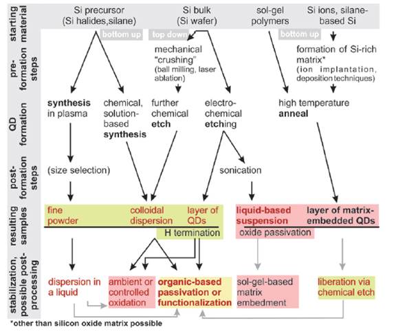
Figure 3 shows an overview of the steps usually followed for the generation of free-standing Si-NCs. Through these techniques is possible to have a good control of the Si-NCs size and shape [104] and to synthetize high quality Si-NCs [107] with PL peaks spanning the entire visible spectrum [108, 109] and with a high quantum yield up to 60 [11]. The surface of the Si-NCs can be covered by different species and functional groups [30, 104]. Dasog et al.[109], for instance, have synthetized colloidal Si-NCs of 3-4 nm in diameter functionalized with alkyl, amine, phosphine, and acetal functional groups. They proved that the PL of the Si-NCs can be effectively tuned across the entire visible spectral region without changing particle size, thus elucidating the role of surface termination. Doped Si-NCs with diameter down to 3 nm have been synthetized using different strategies [89, 90, 110, 111, 112, 113]. Among all, Fujii and coworkers developed an efficient procedure [114, 115, 116, 117, 118, 119, 120] where Si, SiO2, P2O5 or B2O3 were simultaneously sputter-deposited and then annealed in N2 gas atmosphere. During annealing the B- or P-doped Si-NCs were grown in borosilicate (BSG) or phosphosilicate (PSG), i. e. B- or P-doped silica, glass matrices. Then the Si-rich BSG or PSG films were peeled from the plates and annealed in a N2 gas atmosphere to obtain Si-NCs embedded in BSG or PSG matrices. To isolate Si-NCs from the matrices, these films were dissolved in HF solution in ultrasonic bath. This process led to a HF solution containing isolated Si-NCs, that were separated from the solution by centrifugation obtaining in the concentrator a Si-NC powder. Methanol was then added to disperse the Si-NCs.
The properties of free-standing doped Si-NCs have been investigated by absorption, PL and PL excitation (PLE) spectroscopies [109, 110, 111, 114, 116, 121, 122, 123, 124, 125, 126, 127], atomic force microscopy (AFM) [128], atom probe tomography (APT) and proximity histogram analysis [129], electrically detected magnetic resonance (EDMR) [120, 130, 131], electron paramagnetic resonance (EPR) [111, 120, 124, 130, 132, 133, 134, 135], field effect transistor (FET) measurements [136], Fourier transform infrared spectroscopy (FTIR) [124, 125, 126, 127], Kelvin probe force microscopy[128], nuclear magnetic resonance (NMR) [111], Raman spectroscopy [118, 123, 133], secondary-ion mass spectroscopy (SIMS) and inductively coupled plasma atomic emission spectroscopy (ICP-AES) [110, 135], trasmission electron microscopy (TEM) and high-resolution TEM (HRTEM) [111, 114, 116, 120, 123, 125, 127] and, finally, x-ray photoelectron spectroscopy (XPS) [109, 116, 118, 123, 124].
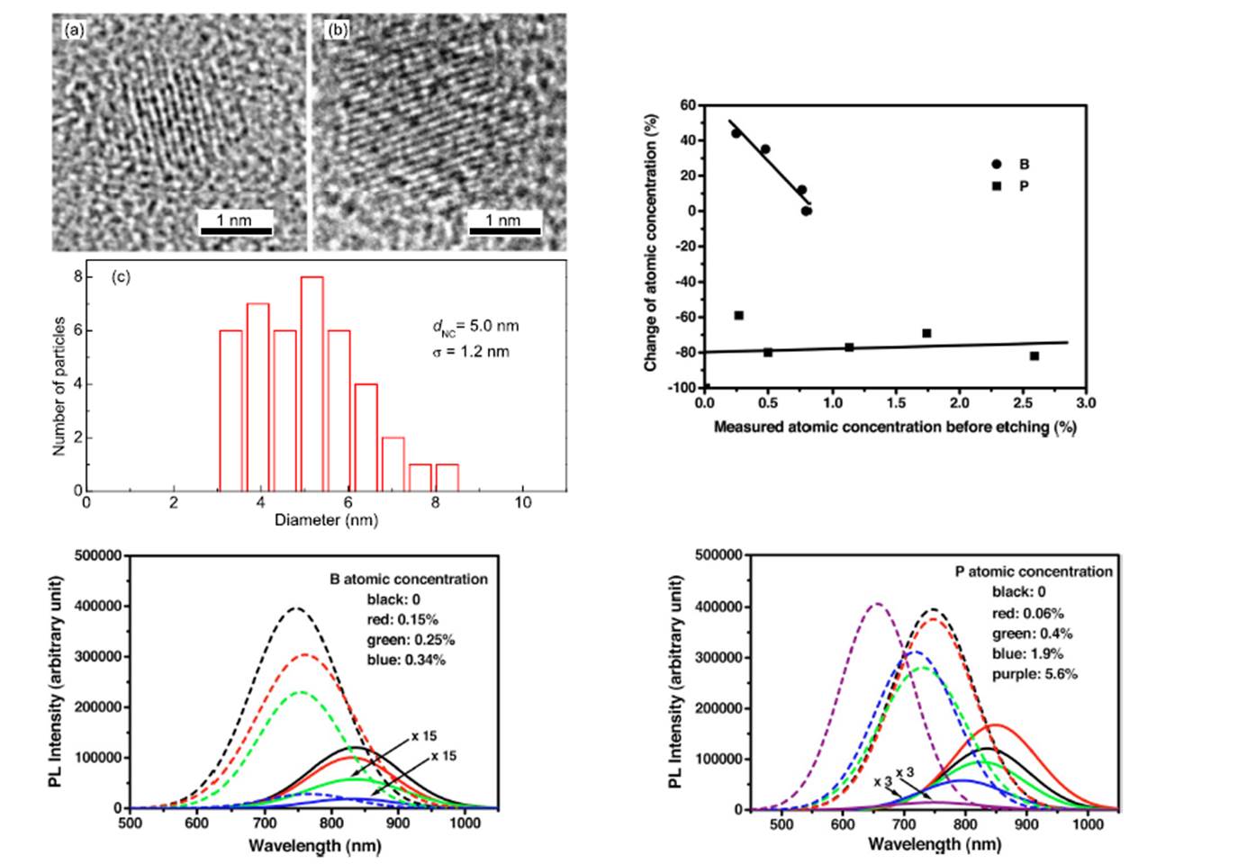
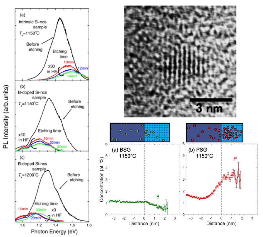
Resuming the experimental information (see Fig. 4 and Fig. 5) one can say that the dopant concentration can be adjusted in a very wide range [110, 123, 133, 135] even if only a small part of the dopants are activated [135, 136, 137]. Moreover doping efficiency depends both on Si-NCs size and on Si-NCs environment [120]. For a review on the experimental results regarding doping efficiency and electrical activity of doped Si-NCs the reader is referred to Refs: [89, 90]. The doped Si-NCs have a good crystallinity, showing that the lattice spacing with respect to undoped Si-NCs is not affected for P-doped Si-NCs, whereas it is slightly reduced for B-doped ones, owing to the smaller size of the B atom [114, 123] (see top left panel of Fig. 4 and bottom panel of Fig. 5)
Experiments pointed out that the hyperfine splitting (HFS) shows a clear size dependence [130] and that impurities are mainly incorporated in substitutional sites [114, 120, 131, 132, 134]. Still regarding the dopant location, several studied pointed out that B atoms prefer to stay in the Si-NC core, whereas P atoms prefer to reside at the Si-NC surface [110, 122, 135] (see top right panel of Fig. 4), even if this result can be reversed depending on the Si-NCs preparation condition [114, 129] (see top right panel of Fig. 5). The PL properties of both B-and P- doped Si-NCs show a shift of the PL maximum to lower energies. Regarding the PL intensity, in the case of B doping there is a decrease with an increase in the doping concentration, whereas for P-doping the intensity becomes smaller at small P concentration and subsequently increases at large concentration [110, 114] (see the bottom panel of Fig. 4 and the left panel of Fig. 5).
3.1 Ab-Initio calculations: formation energies, role of sizes, surfaces, capping species and vacancies
From a theoretical point of view, DFT-based ab-initio calculations for free-standing Si-NCs have been performed in real space [87] or in reciprocal space [138]. The first approach doesn’t show problems connected with spurious interaction between replicas of NCs. The second one, implementing a supercell approach, requires large cells (thus large vacuum regions) to prevent interactions between a NC and its image. Moreover in the case of charged systems, the reciprocal space approach requires a procedure to neutralise the background charge. The dangling bonds at the surface of the Si-NCs are usually passivated with H atoms, which excludes the occurrence of effects induced by the presence of surface dangling bond states and surface reconstructions. Although Si-NCs are usually oxidized, there are numerous experiments where the dangling bonds at the surface are passivated with H [10]. Moreover, as pointed out by several authors, in H-terminated Si-NCs HOMO and LUMO wavefunctions don’t contain contributions from H atoms [62, 64, 93, 139, 140, 141]. As a consequence, changing in the energy gap can be only induced by size reduction (QC effect) or by introducing substitutional impurities.
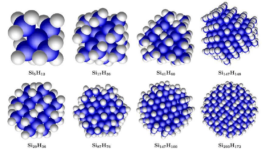
Concerning the shape of the Si-NCs, one can consider both spherical and faceted Si-NCs. The spherical Si-NCs are obtained, from Si bulk, by cutting Si atoms outside a sphere of a particular diameter, whereas the faceted Si-NCs result from a shell-by-shell construction procedure, in which one starts from a central atom and adds shells of atoms successively. Figure 6 shows a cartoon of faceted and spherical Si-NCs.
In the Si-bulk crystal B and P impurities replace substitutionally Si in the lattice and show sp3 hybridization, while in Si-NCs the dopant atom could be either inside or at the surface. Therefore in the case of Si-NCs the considered dopant locations are all the substitutional sites, starting from the center of the Si-NC and moving the impurity to the other substitutional sites in the entire Si-NC (one follows this procedure because both EPR [134] and EDMR [131] have demonstrated that impurities are not interstitials). By taking into account only one impurity per Si-NC one can simulate a wide range of high doping concentrations, which vary approximately from 2x1020 cm−3 (1 mol) to 7x1021 cm−3 (20 mol).
Starting from a SinHm-NC the formation energy for a neutral X impurity can be defined as the energy needed to insert the X atom with chemical potential within the Si-NC after removing a Si atom, that is:
| (1) |
where E is the total energy of the system, is the total energy per atom of bulk Si, and is the total energy per atom of the impurity.
Before looking at the results of the formation energy, it is interesting to look at the changes induced on the structural properties by the presence of an impurity placed at the centre of the Si-NC [80, 80, 92, 142, 143, 144]. After ionic relaxation performed without symmetry constraints, the first neighbors of the impurity in the Si-NC experience different displacements. For the B-doped Si-NCs, while the Si-Si bond lengths remain almost unchanged, some reconstructions occur around the impurity. The overall structure has symmetry, with an impurity displacement along the direction. Such displacement leads to one longer and three shorter and equal Si-impurity distances. While the longer bond is “almost” independent on the Si-NC size, the shorter one increases with the Si-NC size. It is interesting to note that, instead, the relaxation of a bulk Si supercell containing the B impurity leads to an “almost” configuration, in which the four B-Si bonds are practically the same. The relaxation of the P-doped Si-NCs leads to a nearly symmetry, in which the differences between the four P-Si bonds are negligible. This means that, for doped Si-NCs, there is a difference in the behavior between trivalent and pentavalent atoms, i.e. the amount of the relaxation around the impurity is directly related to the impurity valence. Concerning the dependence on the shape of the Si-NCs, the differences of bond lengths are clear. As a rule, the Si-X bond lengths of faceted Si-NCs are longer than the ones calculated for the spherical ones, even when they have similar average radii.
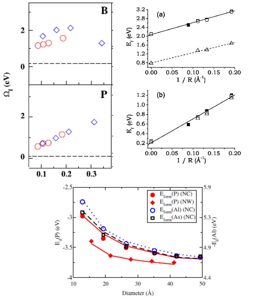
Formation energies, calculated from Eq. 1 and reported in Fig. 7, are strongly connected with the structural properties of the system. For B and P, the formation energy decreases as the Si-NC size increases, thus showing that larger Si-NCs can more easily sustain the B- or P-doping. It also shows an almost linear dependence on the reciprocal radius of the Si-NCs. A comparison between faceted and spherical Si-NCs shows that the incorporation of a B impurity costs more energy for the faceted Si-NC, whereas is nearly shape-independent for P. For both B- and P-doping the impurity formation energies are always higher in Si-NCs than in Si bulk. Moreover, for similar radius, calculations pointed out that B incorporation cost more than P segregation, in agreement with experimental outcomes [110]. Similar results have been obtained by other authors, confirming that the effect of size is much more evident for B-doping that for P-doping. [80, 84, 144, 145, 146, 147, 148, 149].
It was also possible to bring out the role of the relaxation with respect to that of Si-NC size (see Fig. 7). Three different sets of data were presented and discussed [81]. In the first situation (filled squares) the total energies were calculated keeping the Si-Si and Si-impurity distances fixed at the Si-Si bond length of bulk Si. In the second case (empty circles) the undoped Si-NC was firstly relaxed, and the optimized geometry was used for the doped Si-NC, thus neglecting the effects of the relaxation around the impurity. In the third situation (empty triangles) the doped Si-NC was fully relaxed after the insertion of the impurity. Looking at the results of Fig. 7, the atomic relaxation around the B impurity induces a significant reduction of the formation energy, which is nearly independent on the nanocrystal size. The same reduction is observed for P-doped Si-NCs, even if it is much less evident. Moreover, for impurity atom located at the Si-NC center, the variation of the formation energy with 1/R cannot be attributed only to the atomic relaxation around the impurity. This behavior is strongly connected with the QC effect and appears even without any relaxation (see the filled squares).
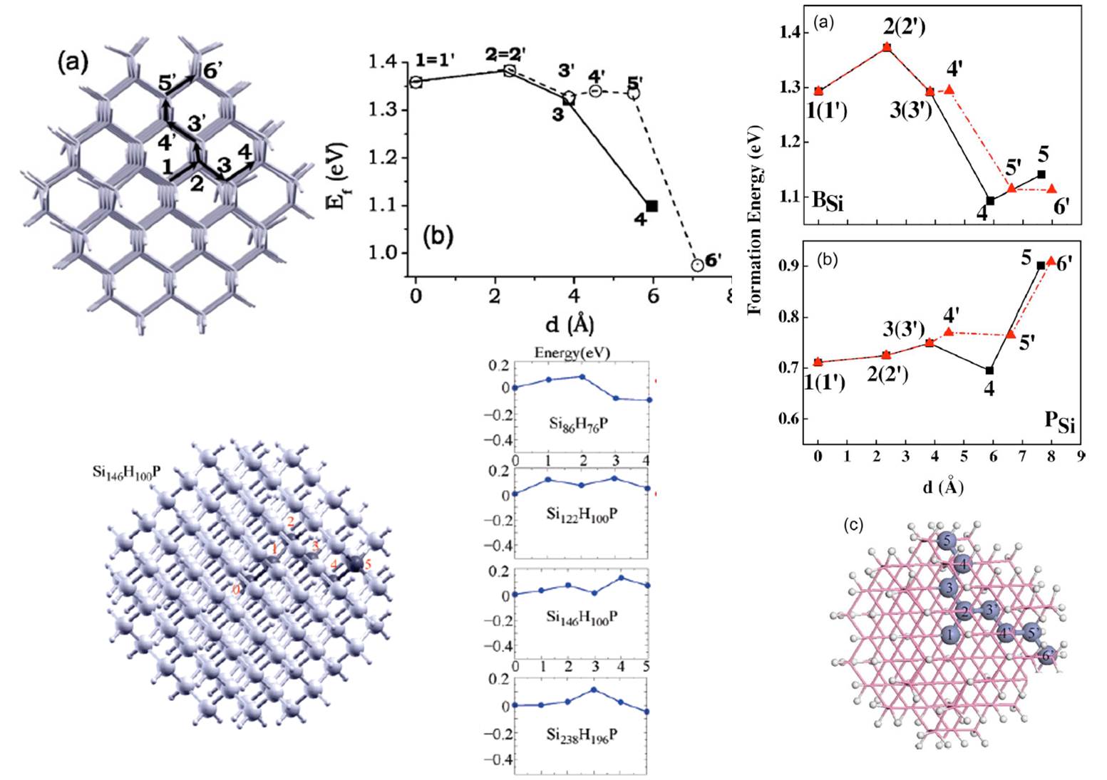
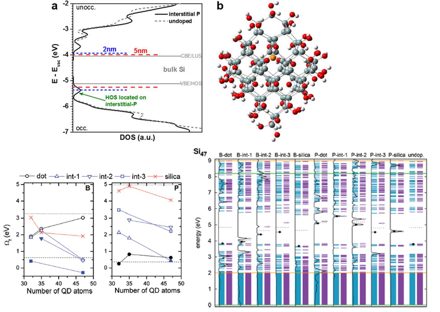
Important efforts were dedicated to the analysis of the formation energies as a function of the impurity position within the Si-NC [80, 81, 145, 150, 151]. This is an important point because the optical and electrical activities of the dopant atoms depend on their positions. Figure (8) (top) shows the formation energy for the B neutral impurity in a Si146BH100-NC [81]. The impurity is moved from the Si-NC center toward the surface along two paths. Since in the experiments the Si-NC surfaces depends on the synthesis conditions, impurity atoms directly located at the Si-NCs surface, i.e. bonded to H atoms, were not considered. The results show that the B atom tends to migrate toward the subsurface position. This is explained by considering that such positions are the only ones that allow a significant atomic relaxation around the impurity, because in the other cases the surrounding Si cage is quite stable. Thus, as the B atom is moved toward the surface the formation energy decreases, making subsurface positions more stable. The preference of B to be incorporated subsurface has been experimentaly established in the case of B-doped Si-NCs passivated by deuterium [121]. The bottom of Figure (8) shows the corresponding results for a P impurity [151]. It is clear that, in this case, for Si-NCs, whose diameter is smaller than about 2 nm, P tends to substitute Si near the surface. Otherwise, the Si-NC center is the energetically most favorable position. Similar results for B and P dopants are shown in the right panel of Fig. 8 [150].
These results have been interpreted in term of a self-purification effect for the smaller Si-NCs: below a diameter of about 2 nm the impurity atoms will be energetically expelled toward the surface and will be hardly incorporated [80, 83, 81, 144, 150, 152].
In particular, Chan et al. [84, 152] showed that this effect can be related to both the binding energy (BE) of the dopant (see below) and the interaction of the dopant with the surface. The binding energy contribution always originates a energy minimum at the Si-NC center, while the strain induced by the dopant dominates energy considerations at the surface. The competition between these two effects dictates the presence or not of self-purification effects.
However, the self-purification effects can be strongly influenced by the presence of defects, vacancies or different capping species used to saturate the dangling bonds at the interface; this fact explains the efficient incorporation of dopant atoms in small Si-NCs with diameter less than 2 nm [129, 153, 154, 155, 156].
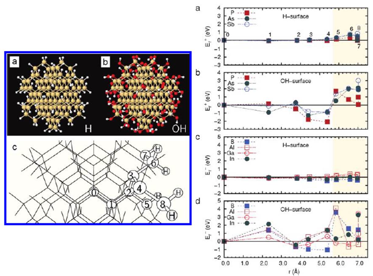
In this context, for example, Chelikosky’s group [157] showed that the mechanisms that move the B atom towards the Si-NC surface depend on the presence of a vacancy located at the center of the Si-NC. Vacancies can be formed more easily as the diameter of the Si-NC decreases and, in the presence of a vacancy that relieves the dopant induced stress, the B impurity prefers to stay in the vicinity of the vacancy, thus becoming more stable in the core of the Si-NC and mitigating the self-purification effect. Ma et al. [158] have studied how imperfections in the passivation of the Si-NC surface influence the dopant formation energy. They considered a faceted Si147H100-NC and they removed a H atom at the surface. The obtained results pointed out that, contrary to the full H-passivated case, the P impurity tends to substitute the Si atom with the dangling bond at the surface. On the contrary, the B atom still prefers to stay in a subsurface position, near to the unpassivated Si atoms. In a series of works Pi et al. [110, 159, 160, 161] demonstrated that, for a substitutional P impurity located at the Si-NC surface and possessing different bonding configurations, the most stable structure is obtained when P is not passivated by H while, in the case of B impurity, the most stable configuration is obtained when B is bounded with two H atoms. Moreover the formations energies for the B-doped Si-NCs are about 1 eV higher than those calculated for the corresponding P-doped cases, showing again that the incorporation of B impurities is less efficient than the incorporation of P impurities. Finally the role of a different Si-NC termination, namely silanol OH group, has been investigated[162, 163, 164, 165, 166]. Carvalho et al. [162], for instance, considered the OH-terminated Si86H76-NC (about 1.5 nm of diameter) that was obtained by replacing H capping atoms with OH groups. Through the calculation of the dependence of the formation energy on the dopant site, an important difference between hydride- and silanol-terminated Si-NCs emerged (see Fig. 9). As in previous studies [80, 81] their results pointed out that for H-terminated Si-NCs the P impurity prefers to stay in the core of the Si-NC, whereas for the B impurity the subsurface positions are the preferred. However in the case of OH-terminated Si-NC, the variation of the formation energy with respect to the impurity site occupation is much larger (of the order of 3 eV) than in the case of the Si-NC terminated by H atoms (of the order of 1 eV). Moreover on going from H-terminated to OH-terminated Si-NCs, whereas the B impurity still prefers the subsurface positions, this position become also preferred by the P impurity. Indeed in both cases the surface positions, where dopants form bonds with oxygen, are in general not the favored ones.
All these results show how the properties of doped Si-NCs strongly depend not only on the Si-NC size but also on Si-NC surfaces and interfaces.
As discussed before from the experimental point of view it is difficult to obtain information about the exact dopant location, nevertheless different techniques have been employed to this task. Regarding as-grown doped Si-NCs sequentially oxidized and HF etched [110] it seems that, in contrast with the theoretical results for H-terminated Si-NCs, B prefers to stay in the Si-NC core whereas P prefers to stay at the Si-NC surface. Nevertheless theory has proven that, for what concern the H-terminated Si-NCs with H deficiencies, the P impurity prefers to be located at the Si-NC surface and B in the core [158], in agreement with the experiments. Moreover, it is well know that experimental results depend on the Si-NCs synthesis procedures. This was confirmed, for instance, by Sugimoto et al.[114] which demonstrated that, by changing the etching time, it is possible obtain Si-NCs with an intrinsic core and a heavily B-doped shell. Moreover, as underlined by several authors [79, 123, 158], whereas the theoretical results concern the thermodynamic stability of the impurity atoms in the Si-NCs, in the experiments is not possible to separate the equilibrium properties from the kinetic effects, which play an important role with respect to doping.
Finally a systematic study of the plasmonic properties of Si-NCs doped with B and P through localized surface plasmon resonance demonstrated that the dominant doping mechanism for P is substitutional doping, whereas for B is surface doping [124].
3.2 Ab-initio calculations. Activation energies, impurity states, optical properties
As in the case of bulk Si, doping of Si-NCs is performed in order to tune their electronic properties. However, the simple incorporation of B or P impurities in the Si-NCs does not ensure the generation of free majority charge carriers by ionization of the dopant atom at room temperature. In a Si bulk system the extra hole associated to the B impurity creates an acceptor level, whereas for P impurity the extra electron creates a donor state. The activation of the impurities, of these states, is related to their binding energy (BE). The BE of the acceptor within a bulk crystal is defined as the energy difference between the defect level and the valence band maximum (VBM), whereas the BE of the donor is given by the energy difference between the conduction band minimum (CBM) and the defect level. In Si-NCs, as stated in Section 1, as consequence of QC effect, size reduction results in a enlargment of the band gap, consequently after doping the relative position of the defect energy level with respect to VBM and CBM strongly depends on the Si-NC size [150]. Moreover, differently from the bulk, the extra hole or electron tends to remain localized near the impurity[80, 82].
A more precise definition of the BE at the nanoscale is given by the impurity activation energy [80, 81, 143, 167]
| (2) |
| (3) |
where and give the Si-NC ionization energy and electron affinity, respectively, while the subscripts and refer to the pure (undoped) and doped system, respectively. The activation energy represents the energy required to ionize the P-doped Si-NC by removing an electron minus the energy gained by adding the electron to a pure Si-NC. Therefore, the ionization energy is given by
| (4) |
where is the number of electrons in a neutral P-doped Si-NC and and are the total energies of the ground state for the neutral and positively charged P-doped Si-NC. The electron affinity of undoped Si-NCs is given by
| (5) |
where and ) are the ground state total energies of a neutral and negatively charged Si-NC, respectively. Similar equations can be derived for the B impurity.
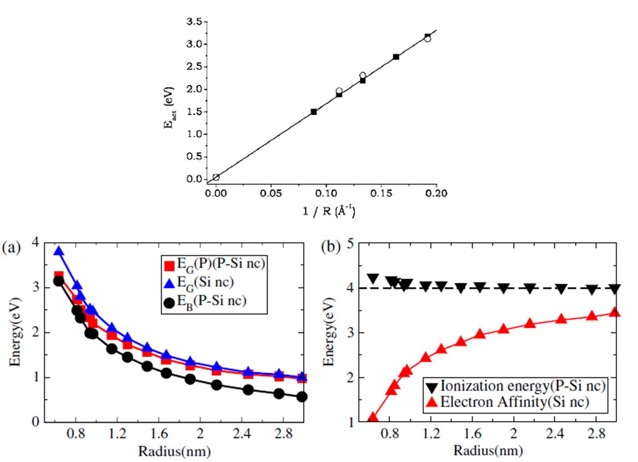
Calculated for B- and P-doped Si-NCs, with dopants located at the nanocrystal center, as a function of the Si-NC size are shown in the top panel of Fig. 10. The figure shows that scales almost linearly with the inverse of the Si-NC radius [81], indicating that the main contribution to is mainly due to the almost unscreened Coulomb interaction. This is a consequence of the reduction of the screening that is observable moving to the nanoscale [168] and that also leads to a strong localization of the impurity states [80]. The calculated activation energies for P-doped Si-NCs [81] are in fair agreement with those calculated in Ref. [80] and showed in the bottom panel of Fig. 10.
Here it is interesting to note that the behavior of the activation energy is mainly due to the decrease with size of the Si-NC electronic affinity, whereas the ionization energy depends weakly on Si-NC size. It is worthwhile to note that investigations by magnetic resonance of the P hyperfine splitting in doped Si-NCs [130] showed that the donor localization is dominated by a reduction in dielectric screening for Si-NCs with radii above 6 nm, whereas for radii below 2 nm quantum confinement dominates. In the intermediate region both dielectric and quantum confinement contribute to the donor wave-function localization. Finally a screening model, based on the Thomas-Fermi theory has highlighted the importance of surface polarization effects. The activation energies of the impurities calculated with this model are in close agreement with the ones obtained using the most computational demanding ab-initio procedures [169, 170, 171]. All these evidences show that in Si-NCs the impurity activation energies are quite large with respect to their Si bulk value (0.045 eV for both B and P), demonstrating that the impurity ionization in Si-NCs is strongly quenched with respect to the bulk, in agreement with the experiments [76, 133, 134]. The activation energy rapidly decreases by increasing the Si-NC size, as confirmed by the activation of P-dopants for large Si-NCs, observed by Kelvin force probe microscope (KFPM) [128].
The calculated dopant activation energy depends not only on the Si-NC size, but also on the position of the dopant atom in the Si-NC. On going from the Si-NC center to the Si-NC surface, shows variations up to 0.2 eV [80, 81, 84, 172]. Moreover by increasing doping concentration, strongly increases, as a consequence of the enhanced structural relaxation induced by the dopants in the Si-NC [173].
The knowledge of the impurity wave-function localization allows the calculation of the hyperfine splittings (HFS), which can detect the presence of dopants in electron paramagnetic resonance (EPR) experiments. Calculations of the HFS for P-doped Si-NCs with diameter up to 6 nm (impurity at the Si-NC center) [84] show a good agreement with the experimental results [174, 175]. Moreover the variations of the HFS calculated values with respect to the dopant position in Si-NCs give another indication of the possibility to obtain Si-NCs with P impurity localized in the Si-NC core.
It is interesting to note that, in the calculations of the vibrational properties and Raman spectra of P-doped Si-NCs [176], it has been found that i) the Si-NC vibrational density of states is only slightly modified by the presence of P-dopant atoms, regardless of its location, ii) the Raman spectra of doped Si-NCs are enhanced with respect to the undoped ones and are strongly dependent on the P-dopant position. Raman spectroscopy may, thus, be used as a method for characterizing not only Si-NC diameter, but also dopant location within the Si-NCs.
The theoretical results for the optical properties reflect the outcomes relative to the energy level diagrams [125, 139, 142, 172, 173, 177, 178]. Since group III and group V doped Si-NCs have an odd number of electrons, usually spin polarized calculations are performed. The relative position of the defect energy level, calculated with respect to the HOMO and LUMO states of the undoped NC, strongly depend on the Si-NCs size. In particular, an increase of the QC, which means a decrease of the Si-NC size, leads to the formation of deeper impurity levels [142, 150]. Moreover, differently from the bulk, the extra hole, or electron, tends to remain localized near the impurity[80, 92]. The impurity level with the lower energy (spin-up or spin-down) is occupied, while the level with higher energy is not occupied. Besides, the increase of the QC induced by size reduction leads to an enhancement of the differences in energy between the spin-up and spin-down impurity-related levels.
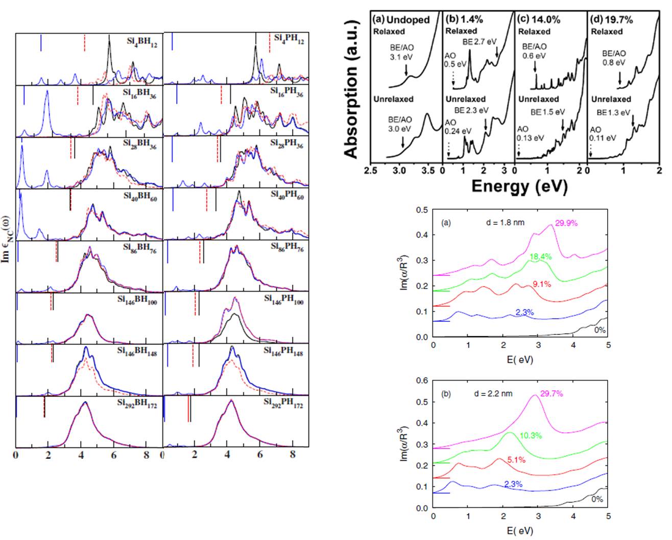
Figure 11 collects some theoretical results concerning the optical absorption properties. On the left we see that the lowest transition energy of the neutral B-impurity tends to zero, as the size of the doped Si-NCs increase. Moreover, the oscillator strength of this transition tends to decrease for large doped Si-NCs. The values of the lowest transition energies of the Si-NCs doped with the ionized B-impurity approach the lowest transition energy of the undoped Si-NCs. For the largest B-doped Si-NC the absorption spectrum looks practically the same of the undoped Si-NC. This shows that changes in the optical spectra of B-doped Si-NCs should be caused by neutral impurities. PL spectra due to the transition from the conduction band to the impurity level have been observed for B-doped free-standing Si-NCs (see discussion above regarding the experimental outcomes). Concerning P-doped Si-NCs the impurity-related peaks in the absorption are not so intense as in the case of B-doped Si-NCs. Moreover the values of the lowest transition energies of the Si-NCs doped with an ionized P atom are larger than the lowest transition energy of the Si-NCs doped with a neutral P impurity and resemble the ones of undoped Si-NCs. For large Si-NCs the role of the P doping is predicted to be more important with respect to that of B doping since the B-related peaks practically vanish for the largest Si-NC, in contrast to the P-related peaks.
Spin polarization plays clearly a role on the spectra of doped Si-NCs. Since the number of electrons in the two groups of spin states differs by one, the HOMO and LUMO of each group of states differ in energy. The minority-spin group of states has one electron less and its HOMO and LUMO are very close in energy, whereas the HOMO-LUMO energy difference of the majority-spin states corresponds roughly to the energy difference between the impurity level and the LUMO of the undoped system. The HOMO-LUMO transition of the minority-spin states presents a very high oscillator strength, and the transitions involving the impurity state and states below the HOMO give rise to intense peaks in the absorption. On the other hand, the spectra corresponding to the majority-spin states are very similar to the one of the undoped Si-NCs [177].
Also the dopants concentration and the induced structural deformation play an important role regarding the optical properties of doped Si-NCs. By means of a TDDFT study it has been showed (see top right in Fig. 11) that for structurally unrelaxed P-doped Si-NCs, sub-band absorption, related to electronic excitations from impurity, is induced by the presence of deep energy levels in the low energy region [173]. By increasing dopant concentration both the absorption onset and the band-edge absorption red-shift. Experimentally infra-red (IR) absorption has been observed in P-doped Si-NCs togheter with a red-shift of the PL [35]. After structural relaxation of the system [173] the situation does not change very much for lower dopant concentration. Anyway, an increase in the dopant concentration induces increasing structural relaxation, that remove deep impurity states from the band gap region (i.e. absorption onset and band-edge absorption coincide). Moreover a slight blue-shift is calculated at larger concentration. Tight-binding calculations [178] pointed out another interesting consequences of hyperdoping. By calculating the optical response of Si-NCs ideally doped with different and large concentrations of P atoms, a collective response of P-induced electrons was proven. This leads to localized surface plasmon resonance phenomena, ideal for the development of Si-based plasmonic devices, enabling silicon-compatible IR photonics at the nanoscale [125, 137].
4 Matrix-embedded Nanocrystals
Matrix-embedded Si-NCs offer advantages in terms of stability and low-cost manufacturability. Moreover they can be exploited to develop CMOS compatible devices and novel third-generation photovoltaic systems. Methods for the fabrication of matrix-embedded Si-NCs are the plasma enhanced chemical vapor deposition (PECVD) [179], the reactive magnetron sputtering [180], the ion implantation [181] and the formation of superlattices of alternating SiOx and SiO2 layers (see Fig. 3, for scheme of the different techniques used) [67, 182, 183]. Unfortunately, the high resistivity of the embedding matrix reduces the possibility to employ such materials in applications that require a high carrier mobility. For this reason, the possibility to introduce dopants has been explored in order to improve transport and other fundamental characteristics [78, 79].
For matrix-embedded Si-NCs the doping of nanostructures involves additional complications arising from the presence of both interfaces and materials with different affinities in hosting the dopant species [85]. In practice, experimental samples of matrix-embedded Si-NCs present inhomogeneous impurity concentrations that depend on the fabrication technique. In other words, since dopants tend to diffuse during the fabrication process, one cannot simply limit the doping to a selected region of the material. Therefore, in order to connect some physical results to the presence of dopants, we have to understand where the impurities are located, that is if they are in the nanostructures, at the interfaces or in the embedding matrix.
To accomplish this, many experimental techniques have been employed, together with ab-initio calculations.
Fabrication of doped Si-NCs follows two main procedures. In the first one, doping occurs during the Si-NCs synthesis, i.e. the dopants are incorporated without additional steps. In the second one, instead, doping occurs after the Si-NCs synthesis.
The first report of B and P doping performed during Si-NCs synthesis was due to the group of Fujii [186]. Si, SiO2, P2O5 or B2O3 were simultaneosuly sputter-deposited and then annealed in N2 gas atmosphere. During the annealing the B- or P-doped Si-NCs were grown in BSG or PSG, i e. B- or P-doped silica, glass matrices [35, 77, 120, 129, 155, 174, 175, 184, 185, 187, 188, 189, 190, 191]. The doped Si-NCs were investigated by HRTEM [185, 186, 189, 191], Raman[186], ESR [120, 174, 175, 192] absorption and PL spectroscopies [35, 77, 174, 175, 184, 185, 189, 191, 192], ATP and proximity histograms, that enable the visualization of the Si-NCs structure as well as of the dopant distribution with subnanometer resolution [129].
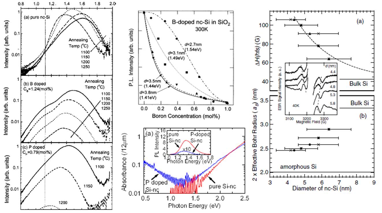
The obtained results pointed out that the presence of impurities during the synthesis affects the growth kinetics of the Si-NCs, resulting in a wide size distribution that depends on the annealing temperature and on the nature and concentration of dopants. Doped Si-NCs with a diameter ranging from 2.7 to 3.8 nm, slightly larger than the corresponding undoped Si-NCs grown using the same annealing temperature, were prepared [79]. The doped Si-NCs showed good crystallinity and were well separated from each other in the matrix. The PL spectra showed a quenching in the intensity (top center panel of Fig 12). For B doping, the quenching was found to increase with the NC size. This behavior was explained by assuming that B impurities were localized in substitutional sites in the Si-NCs and that they were responsible to promote non-radiative recombination mechanisms (Auger recombination) of trions formed by the photogenerated e-h pairs and the B-induced hole. Concerning the PL activity in P-doped systems, two opposite trends were recorded. Initially an increase in the PL intensity was detected, then, on increasing the P concentration, a decrease of the PL intensity was recorded. Also in this case this PL quenching was explained in term of Auger recombination, whereas the initial PL intensity increase was assigned to P passivation of the dangling bonds at the interface between the Si-NCs and the matrix.
In both cases, the PL spectra became broader, indicating the development of low energy features with respect to the undoped case (left panel of Fig. 12). Optical absorption in the infrared region, was observed for P-doped Si-NCs. In this region of frequencies, absorption increases when the P concentration increase and seems to be not affected by the presence of the PSG matrix. This effect was interpreted as the consequence of intra-conduction band transitions (bottom center panel of Fig 12) induced by the presence of the impurities. Quantum confinement of P donors in Si-NCs was evidenced through the clear dependence of the hyperfine splitting on the Si-NC size (left panel of Fig 12). Regarding the impurity location, APT and proximity histogram [129] revealed incorporation of B and P into the Si-NCs with clear differences. The B concentration sligthly decreased on going from the matrix to the Si-NC interfaces and from the Si-NC interfaces to the NC core. The P concentration started to increase about 1 nm far from the Si-NC interface, reaching a maximum in Si-NC core (see bottom panel of Fig 5).
B- and P-doped Si-NCs formed as multilayers in a SiO2 matrix have been fabricated, aiming at the development of silicon quantum dot based solar cells [40, 66, 155, 193, 194, 195, 196, 197, 198, 199, 200]. B-doped Si-NCs were formed by magnetron co-sputtering of Si, SiO2 and B2O3 targets, while for P-doped Si-NCs, Si, SiO2 and P2O5 targets were used. Doped Si-NCs were fabricated by PECVD using the superlattice approach, that permits to well control the size and the distribution of the Si-NCs [153, 154, 156, 201, 202, 203, 204, 205, 206, 207, 208, 209, 210, 211, 212]. The dopants location and the doping effects were studied through SIMS [196, 197, 201] and time-of-flight-SIMS (ToF-SIMS) [153, 209, 211], XPS [153, 154, 193, 207, 210], FTIR [66, 193, 195], TEM and HRTEM [40, 153, 193, 195, 198, 205, 207, 209, 210, 212], ESR [199, 205], glancing incidence x-ray diffraction (GIXRD) [40, 193, 200], absorption and PL spectra [40, 153, 193, 195, 199, 200, 201, 205, 206, 208, 212], XPS [195, 198, 205, 207], XANES [204], Raman [198, 205, 212], Rutherford backscattering spectrometry (RBS) [209] and APT and proximity histogram analysis [155, 202, 204, 208].
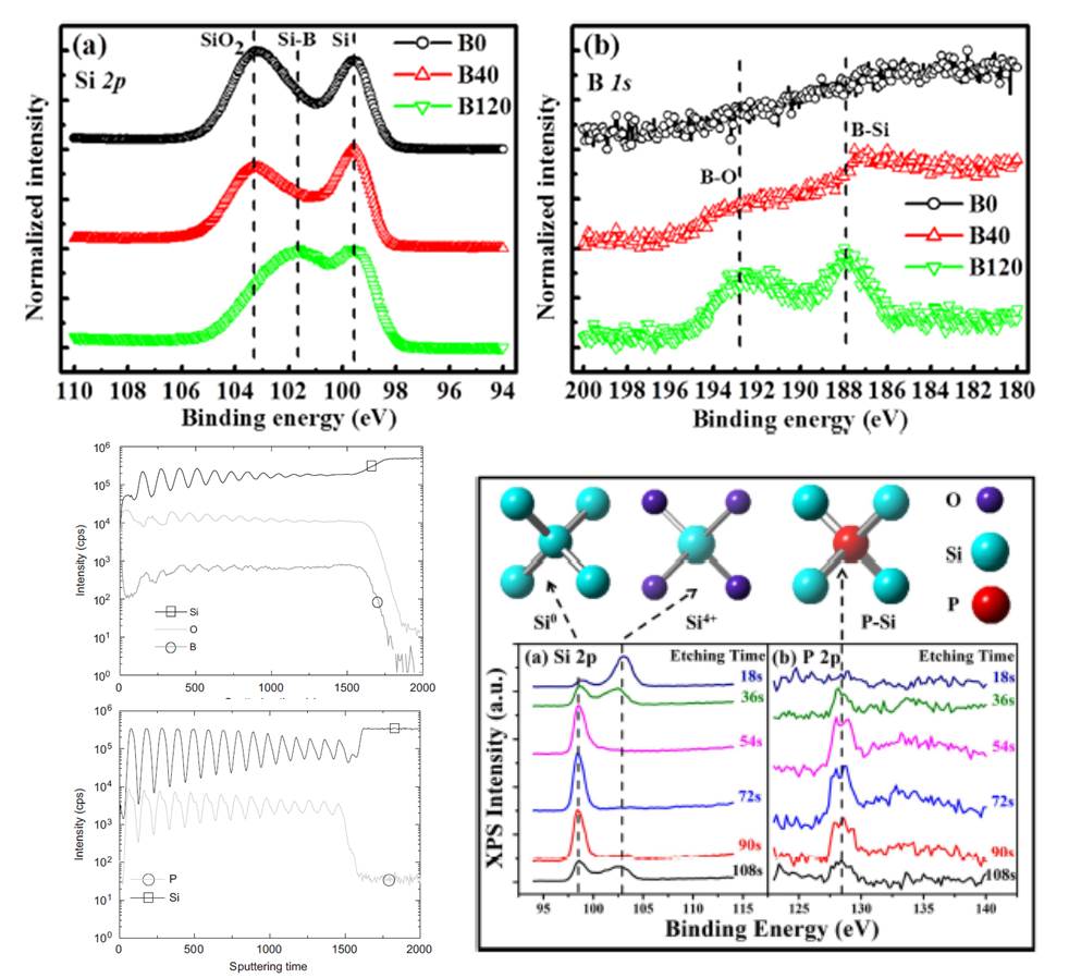
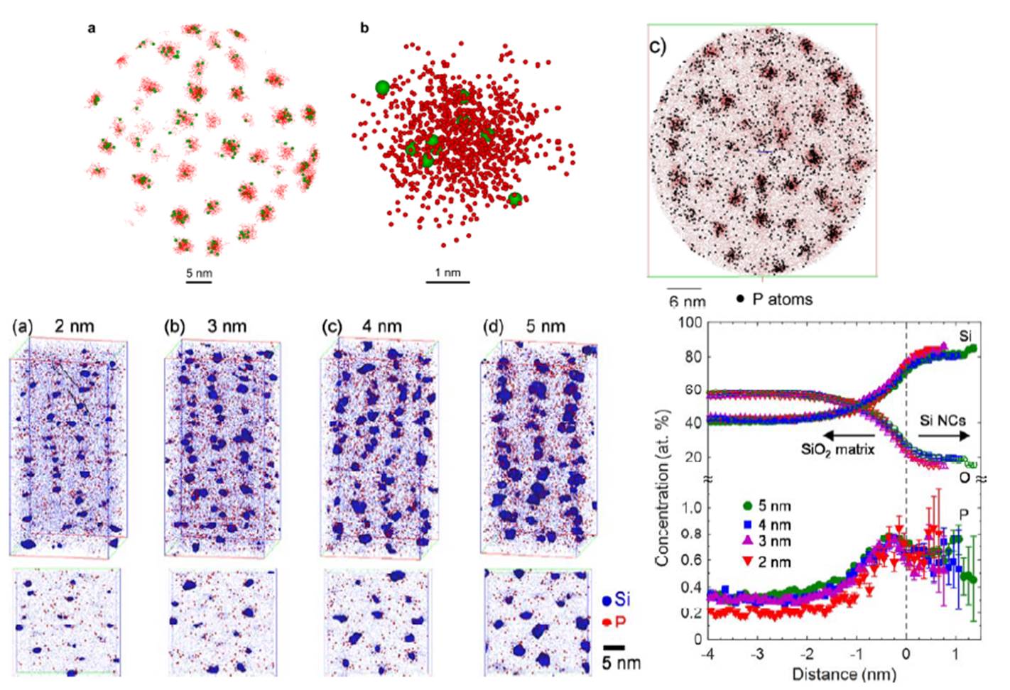
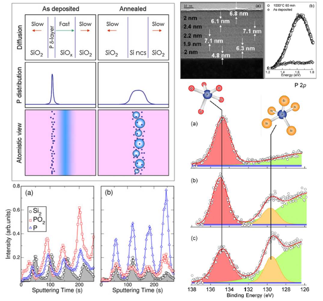
The behavior of the PL spectra was found to be similar to those of the doped Si-NCs embedded in BSG and PSG. SIMS data suggested that the dopants were located in the silicon layer and not in the silica layer [66, 193] (see Fig. 13, bottom left panel), while XPS data pointed out that B is either inside or at the surface of the Si-NCs, with a concentration equilibrium distribution of B between the Si and the SiO2 [198] (see Fig. 13, top panel). In the case of P, the XPS spectra suggested that most of the P atoms were located in the Si layer and at the Si/SiO2 interface [205] (see Fig. 13, bottom right panel). Even after high temperature annealing, P atoms did not tend to move into the SiO2 layer and were better incorporated in the Si-NCs [154, 209, 210]. APT and proxigram analysis were used to determine the dopants localization. Gnaser et al. [202] founded that the concentration of P was enhanced in the region of Si-NCs with a maximum at the Si/SiO2 interface; their results seemed to indicate the occurrence of self-purifications effects. Nevertheless the incorporation of P atoms in very small Si-NCs with diameter as small as 2 nm was demonstrated by the same group [156] (see Fig. 14). This result was confirmed by Perego et al. [153, 154] that, using a combination of TEM, ToF-SIMS and XPS, showed that P atoms are definitevely incorporated within Si-NCs of diameter of the order of 2 nm. These results have been interpreted as a consequence of the favored P diffusion towards the Si-rich region (see Fig. 15).
Indeed it has been demonstrated that ion beam synthesis, which is a well known approach to grow undoped Si-NCs embedded in SiO2, is also an efficient technique to grow doped Si-NCs with diameters of few nanometers, if the dopants are co-implanted with Si [213, 214, 215]. Combining the results obtained by APT, Raman, PL and PLE analysis, the authors concluded that P impurities tend to be efficiently incorporated in the Si-NC core whereas B atoms are mainly localized at the Si-NC/SiO2 interface (see Fig. 14, top left panel) [213, 214, 215].
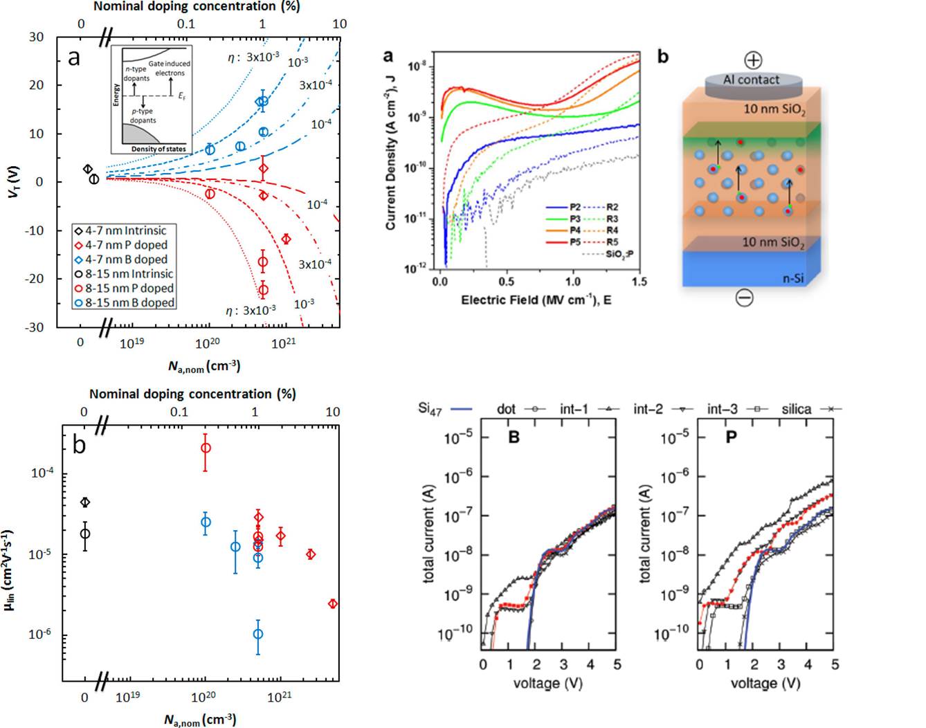
The electrical activity of matrix-embedded doped Si-NCs, monitored by current voltage measurements, demonstrated that majority carriers, originated from substitutional P-donors, must be generated to overcome significant P-ionization energies between 110 and 260 meV. In the absence of electrical fields at room temperature, however, no significant free carrier densities were detected [208].
As a consequence, it has been concluded that only a small fraction of P-atoms are in substitutional sites within the Si-NCs, while the majority of them, reside in interstitial sites. These atoms are considered to be at the origin of the PL quenching that was previoulsy assigned to the occurance of Auger recombination mechanisms [203, 204, 208]. Interestingly Almeida et al. [120] have studied both free and SiO2 embedded P-doped Si-NCs using EPR spectroscopy. Their results showed that P dopant atoms are prevalently incorporated at substitutional sites and act as donors. Moreover the donor electron density decreased by several order of magnitude when matrix-embedded Si-NCs were etched by HF to remove the SiO2 matrix and were subsequently exposed to air. Once more, these results pointed out that doping efficiency depends not only on the dopant location but also on the Si-NCs environment and on the doping strategies. A marked difference in effective mobility for B-doped Si-NCs has been evidentiated in sample obtained by diffusion or by in-situ doping methods, respectively [200].
Doping after synthesis is usually made by ion implantation in Si-NCs formed in SiO2 matrices [216, 217, 218, 219] or delivering a controlled amount of dopant atoms from a spatially separated diffusion source [209, 210, 211] (see Fig. 14). The first strategy suffers of implantation damages. The second, instead, make possible to decouple equilibrium properties from kinetics effects, thus providing, for the first time, results that can be compared directly with the theoretical predictions. These experiments show that high levels of P impurities can be introduced in the Si-NC core, trapped with a binding energy of 0.9 eV.
4.1 Ab-initio calculations. Formation energies and electronic properties
Contrary to the case of doping in H-terminated and OH-terminated Si-NCs, there are very few theoretical investigations regarding the study of doped Si-NCs embedded in a host matrix. The reason is related to the complicated models, characterized by a large number of atoms, that are needed to simulate these systems.
Carvalho et al. [164, 165] modeled the embedded Si-NC considering an approximate spherical Si crystalline core of 1.5 nm diameter, surrounded by a spherical shell of -cristobalite SiO2 with about 2 nm of outer diameter. This Si-NC contained 161 Si atoms and 196 O atoms. To generate a realistic amorphous SiO2 layer and a realistic Si-SiO2 interface, the Si-NC was submitted to an anneal at 1800 K using molecular dynamics simulations. Three different annealing times were used, that is t = 2.0, 2.3 and 2.6 ps (the relative configurations are labelled with I, II and III). The structures obtained from the simulations were subsequently fully relaxed at 0 K, and all the dangling bonds were passivated by H atoms. The new structures were then fully relaxed. The obtained systems were used to calculate electronic properties and dopants formation energies. The adopted procedure led to three different structures: the Si161O196H59-NC for the annealing I and II and the Si161O196H57-NC for the annealing III. As dopants either B (in their negative charge state) or P (in their positive charge state) were considered. The preferred locations for subsitutional impurities were investigated calculating and comparing the energy of doped Si-NCs obtained by replacing B or P for each of the Si atoms in the three situations. The results showed that the doping behavior for Si-NCs covered by a SiO2 shell differs from that of the corresponding H-terminated Si-NCs and that the behavior of P is different from that of B. Whereas the formation energy of B is nearly independent on the impurity location, with average formation energies only slightly lower at the interface, in the case of P doping the dopant has a strong preference to stay in the Si core and not in the SiO2 shell (see Fig. 16 bottom left panel). These outcomes were correlated to the fact that B atoms prefer to stay at interface locations where they form only three short Si-O bonds, while P atoms prefer to form a fourfold coordination with Si atoms.
A different encapsulated Si-NC was obtained by Ni et al. [220, 221]. Starting from the H-terminated Si71H84, they replaced H atoms with oxygens, which were then outwardly bonded by adding Si atoms. Finally, they passivated the system with H atoms to restore a fourfold coordination for all the Si atoms. The final system, that is the Si123O96H100, represented a Si-NC covered by a 0.25-nm-thick SiO2 shell. Effects induced by the presence of dangling bonds at the Si-SiO2 interface were also investigated. The obtained results for the formation energies were in agreement with those of Carvalho et al. [164, 165] for the fully passivated Si-SiO2 systems: B showed a small preference for the subinterface region, whereas P clearly preferred to stay in the Si-NC core. In contrast, when dangling bonds are induced in the system, B preferred to stay at the Si/SiO2 interface. It is important to note that the impurity formation energies are reduced on going from the H-saturated Si-NCs to the embedded ones. Moreover, electronic and optical properties still revealed the presence of deep levels in the band gap and light emission at energies smaller than the energy gap of the undoped system [220] (see Fig. 16 left panel).
Realistic calculations for Si-NCs embedded in a solid matrix were performed by Guerra et al. [166, 222]. SiO2-embedded Si-NCs were generated starting from a 3x3x3 -cristobalite-SiO2 matrix (for a total of 648 atoms), by removing all the O atoms inside a sphere whose radius determines the Si-NC size. The so-obtained Si-NC, embedded in the SiO2, presented perfectly coordinated atoms and the same Si-Si distance of -cristobalite, corresponding to about 3.2 Å. After the relaxation, the Si/SiO2 interface formed strongly stressed bonds, while far from the interface the bulk atomic densities were recovered [68]. Dopant impurities were introduced in a substitutional Si-site located in the Si-NC center, at the Si/SiO2 interface, or in the SiO2 matrix far from the Si-NC. Since the Si atoms at tn interface can be bonded to one, two or three O atoms (i.e., Si1+, Si2+, Si3+), for each structure all the possible oxidation types for the interfacial doping were considered. Each structure was fully relaxed after doping in order to include effects induced by structural rearrangements around the dopant atom.
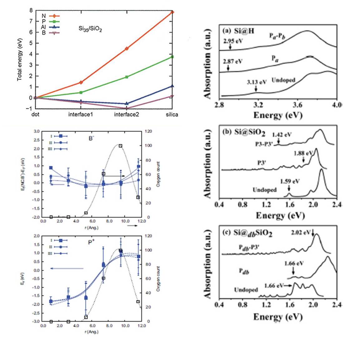
In Fig. 16 (top left panel) the calculated total energies for a Si35-NC (diameter of about 1 nm) embedded in SiO2, single-doped with a group-V (N or P) or a group-III (Al or B) atom placed at different substitutional sites, are shown. In the figure the minimum of each curve identifies the energetically favored site of the corresponding dopant. The data clearly indicate that for n-type doping (P and N) the impurity tends to settle in the Si-NC core, even for very small Si-NCs, confirming once more that dopant formation energies strongly depend on different interfaces. Instead, for p-type doping (Al and B) the interfacial sites are favored. Furthermore, it is clear that in all the considered cases the doping of the SiO2 region is unlikely to occur. In particular, P doping requires a very high formation energy in order to move the dopant atom from the Si-NC core to the silica; this is in agreement with the observation that for Si-NCs embedded in a SiO2 matrix, the matrix provides a strong barrier to P diffusion, inducing P segregation in the Si rich region [154, 210]. By contrast, still consistently with experiments [198], the diffusion of B toward SiO2 is significantly easier. Once more the structural relaxation around the impurity plays a significative role. P atoms maintain a sort of tetrahedral coordination in all the cases, with all the bonds showing approximately constant characteristic lengths with Si and/or O. Instead, B atoms tend to form, when placed at the interface with two O atoms, a strong antibonding with one of the neighbors, causing repulsion to a large distance [166].
Several experimental results based on atom probe tomography and proximity histograms support these tendencies. APT demonstrated that n-type dopants (P and As) are efficiently introduced in the Si-NC core, whereas p-type dopants (B) are located at the Si-NC/SiO2 interface [213, 214]. By proximity analysis Nomoto et al. [129] found significant differences in the B and P distribution profiles. For P-doped Si-NCs, the P concentration increases into the Si-NC region, whereas for B-doped Si-NCs the B concentration decreases moving from the Si-NC interface toward the Si-NC core. It is worthwhile to note that a similar picture has been observed also for doped Si nanowires (Si-NWs). In a joint experimental-theoretical effort it has been shown that, whereas the impurity B atoms are more stable at the Si-NW/SiO2 interface, in a split interstitial configuration at a Si site, P impurities preferentially pile up in the cystalline Si region [223].
As pointed out before, in recent works [204, 208] it has been suggested, based on electronic transport measurements in P-doped Si-NCs, that the impurity atoms are located preferentially in interstitial sites. DFT calculations have been performed for P impurities in SiO2, in SiO0.9 and in Si-NC/SiO2 systems, where the SiO0.9 and SiO2 were simulated through transition Si-O shells capped by hydrogen. The results showed that P-atoms located in interstitial sites generate states in the fundamental gap of Si-NCs (see Fig. 17). In order to explain the observed quenching of the PL in P-doped Si-NCs, authors hypothesized the occurrence of new non-radiative recombination dynamics generated by these interstitial-P induced states, as an alternative procedure with respect the Auger recombination processes. No calculations were made about the formation energies for the P impurity in this interstitial position. It is worthwhile to note that in a recent study devoted to energetic and carrier transport properties of doped Si-NCs embedded in SiO2 [222] it was found that P prefers to stay in the Si-NC and B at the interface, bonded to three oxygen atoms and that, in this last case, the formation energy is even lower with respect to the undoped case.
5 Carrier transport
In this section we will briefly analyze carrier transport in doped Si-NCs, and we will discuss how electric mobility can be used to discern the role played by the impurities.
In order to prove that impurities located in Si-NCs effectively act as dopant, it is necessary to assess their electrical activity. This can be done using, for instance, conductivity and resistivity data [40, 133, 134, 207], current density versus electric field measurements [40, 200, 208, 212, 224], Hall mobility experiments [225] and field effect transistor analysis [136]. Due to the difficulties in the interpretation of the results obtained in transport measurements, that often depend on a large number of concomitant effects (like for instance transport due to defects, the presence of hyperdoping effects and transport in percolated nano-Si networks), today little is known about the effective electronic activation.
From experimental results, it seems possible to conclude that doping depends on synthesis methods and that B and P can dope Si-NCs. However very low dopant activation efficiency were recorded, that is 10-3- 10-6, where the lower limit refers to B (see Fig 18, left panel and top right panel). Theoretically, it has been shown that an increment of the conductivity, calculated with respect the undoped embedded Si-NCs, can be obtained only for P-doping [226]. Instead, the electrical response of B-doped embedded Si-NCs does not differ from the undoped case [222] (see see Fig 18, bottom right panel).
6 Codoping
The main limitation to high PL efficiency in Si-NCs is due to radiationless Auger recombination. This drawback can be circumvented by simultaneous p-type (B) and n-type (P) compensated doping of the Si-NCs [82, 184, 227]. In this section we will discuss the concept of impurity compensation in Si-NCs. We will show that B and P codoped compensated Si-NCs exhibit properties that strongly differ from the ones of the undoped and single doped Si-NCs. Moreover we will prove that codoping can be exploited to tune the electronic and optical properties of Si-NCs, in a highly controllable way.
Codoped Si-NCs were firstly grown by Fujii and coworkers [184, 227] using a co-sputtering method. During the annealing, the Si-NCs were grown in borophosphosilicate glass (BPSG) matrices. The evidence that impurities were located into substitutional sites of the Si-NCs was obtained through infrared absorption spectra [189] and by electron spin resonance (ESR) [184, 190].
The PL spectra of the B and P codoped Si-NCs strongly differ from the ones recorded for both the single doped (B or P) and the undoped Si-NCs [184, 188, 191]. The codoped Si-NCs, for instance, exhibit PL energies red-shifted with respect to those of the corresponding undoped Si-NCs; in particular PL peaks, originated by optical transitions between donor and acceptor states, extend from the visible range to energies below the energy gap of the bulk Si [77, 184, 228].
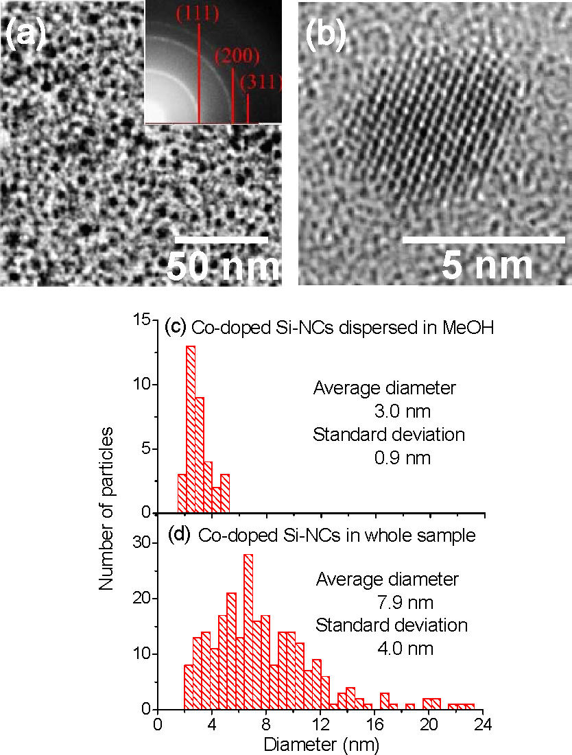
More recently the same group reported a new method to obtain B and P codoped colloidal Si-NCs, where NCs were dispersed in methanol without a surface functionalization process [115, 116, 117, 119]. To isolate Si-NCs from BPSG matrices, the BPSG films were dissolved in HF solution in ultrasonic bath. This process produced isolated Si-NCs dispersed in solution, that were separated from the HF by centrifugation obtaining in the concentrator a Si-NC powder. Methanol was then added to disperse the Si-NCs. Even if the majority of Si-NCs were dispersed in methanol, a fraction of Si-NCs were precipitated. These precipitates were removed by centrifugation and a supernatant liquid was obtained [116]. High resolution transmission electron microscopy (HRTEM) images showed the presence of lattice fringes corresponding to the planes of a Si crystal. Moreover it proved the presence of a large number of defected-free Si-NCs with an average diameter of about 3 nm (see Fig. 19).
An advantage of this method concerns the possibility of producing highly dispersive Si-NCs in polar solvents or water solutions of different PH, without employing organic ligands, thus permitting the use of these Si-NCs for biomedical applications [49]. Figure 20 shows a picture of a methanol solution in which codoped Si-NCs of about 5 nm in diameter are dispersed [229].
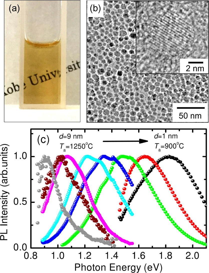
The solution is very clear and light scattering by agglomerates is not seen. The average diameter of the codoped Si-NCs can be varied from 1 to 9 nm controlling the growth temperature and the resulting PL energy peaks range from 1.85 to 0.90 eV. Since after dispersion of the Si-NCs in methanol, the position of the PL peak shifted to slightly higher energy with increasing storage time and then is stabilized, the authors concluded that the surface dangling bonds were terminated by O molecules [117].
Codoping of Si-NCs has been recently obtained also for silica embedded Si-NCs using ion implantation [228], co-sputtering [230] or using B2H6 and PH3 gases in PECVD [231]. In all these cases donor-acceptor pair recombination emission has been clearly observed. Moreover evidence of carrier multiplication were detected [230].
6.1 Ab-initio calculations: codoped free-standing and matrix-embedded nanocrystals
In order to interpret experimental results, we will report the outcomes of ab-initio simulations for B and P simultaneously codoped Si-NCs [65, 82, 92, 145, 146, 147, 166, 177, 232, 233, 234, 235, 236, 237].
Starting from H-terminated Si-NCs, B and P impurities have been located in substitutional positions inside the Si-NCs. Full relaxation of all the obtained structures was then allowed. In Fig. 21 (left panel) the calculated impurity formation energies (see Eq. 1) for the Si85H76-NC and the Si147H100-NC are reported and compared with the ones calculated for B or P single-doped Si-NCs. As an example, in these codoped Si-NCs the dopants are located at two different distances, that is the nearest possible distance between two Si-NC subsurface sites (0.364 nm and 0.368 nm after geometry relaxation for the Si85BPH76 and the Si145BPH100 nanocrystals respectively) and the largest possible impurity distance (B and P located in opposite Si-NC subsurface sites, 1.060 nm and 1.329 nm after geometry relaxation for the Si85BPH76 and the Si145BPH100 nanocrystals respectively).
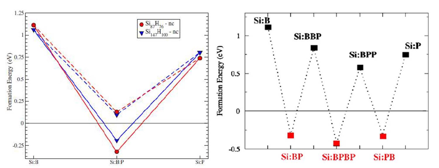
From Fig. 21 it is clear that simultaneous B and P doping strongly reduces (by about 1 eV) the formation energy with respect to both B or P single doped cases and that this reduction is similar for Si-NCs of different sizes. While B or P single doping is very costly, B and P codoping is much easier, independently on the Si-NC size [82, 92]. Moreover a reduction of the distance between the two impurities results in a reduction of the formation energy; its minimum is obtained when the impurities are located at the nearest neighbors positions at the surface of the Si-NCs. In these cases the formation energy assumes negative values. It is interesting to note that Nomoto et al. [129] have observed that codoping is an effective means of promoting segregation and stability of the B and P impurities in the Si-NC region. The fact that Si-NCs can be more easily codoped than single-doped explains the possibility of easely grow B and P codoped Si-NCs [77, 184, 227]. In particular, in the codoped Si-NCs, the differences among the four impurity-Si bond lengths are always smaller with respect to the single-doped case. Thus, if carriers in the Si-NCs are perfectly compensated by simultaneous n- and p-type impurity doping, an almost Td configuration is recovered; in this configuration the four impurity-Si bonds are practically the same [92, 166, 177].
These results are confirmed by the calculation performed in the case of multi-doping [235]. In Fig. 21 (right panel) the calculated formation energies of Si147H100-NC are reported as a function of the number of impurities. We note that the presence of an odd number of dopants (1 or 3) brings the formation energies to higher values. Instead, the presence of an even number of compensated B and P impurities (2 or 4) strongly lowers the formation energies, thus indicating that doping is always much easier to realize when one has the same number of donor and acceptor impurity atoms.
Also the electronic properties of B- and P- codoped Si-NCs are qualitatively and quantitatively different from those of the single doped (B or P) or undoped cases. The presence of both a n- and a p-impurity leads to the formation of a HOMO state that contains two electrons and to the formation of a HOMO-LUMO gap that is strongly lowered with respect to the one of the corresponding undoped Si-NCs. The energy levels for the undoped Si87H76-NC and the codoped Si85BPH76-NC, calculated at the point in the optimized geometries, are shown in the right panel of Fig. 22, where only the levels corresponding to the HOMO, LUMO, HOMO-1 and LUMO+1 states are depicted.
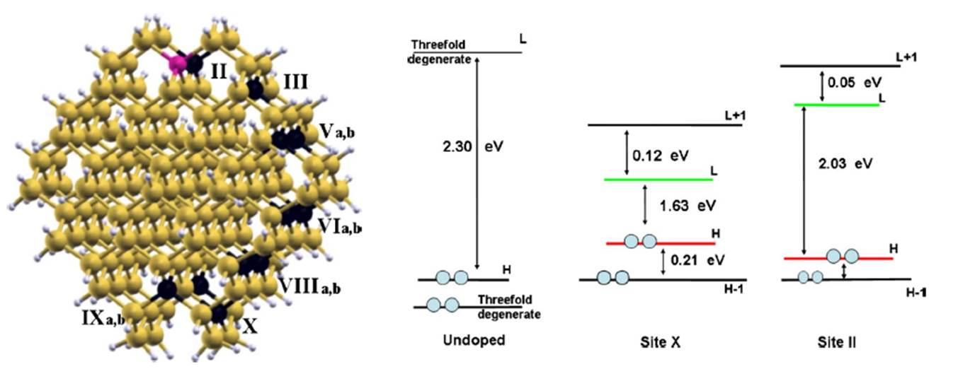
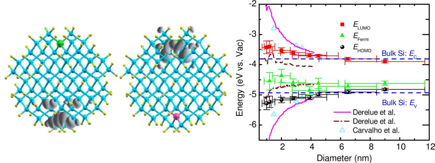
In Fig. 22, left panel, two different distances between the compensated dopants are considered, that correspond to the minimum and the maximum separation between impurities located in subsurface positions. From Fig. 22 it is clear that in both codoped cases the HOMO-LUMO energy gap is always lower than the one calculated for the undoped Si-NCs. Besides, when the impurities are at large distances the energy gap is strongly reduced; this reduction is less evident when the impurities are brought closer, as a consequence of the increased Coulomb interaction. These results underlined that, by tuning NCs size and impurity locations, it is possible to obtain codoped Si-NCs with a gap ranging from the visible range to values below the bulk Si energy gap [92, 177, 235], in agreement with the experimental observations [77, 117, 119, 184, 238]. Results reported in Fig. 22 point out that, in codoped Si-NCs, the HOMO and the LUMO states correspond to the acceptor and donor levels of the B and P impurities. This result is confirmed by the plots of Fig. 23, which clearly demonstrate that HOMO and LUMO wavefunctions are localized on the B and P impurities, respectively. These results are in good agreement with experimental observations, as show in the right panel of Fig. 23 where the HOMO, LUMO and Fermi energies are reported for codoped Si-NCs of different diameters. The experimental HOMO and LUMO energy levels show a clear size dependence that differs from the one predicted by tight binding for hydrogen-type impurities in H-terminated Si-NCs [239], whereas they are in the same energy range of those calculated by ab-initio methods [82, 92, 240].
The reduction of Si-NC energy gap as a consequence of the simultaneous presence of B and P impurities is also confirmed by DFT calculations of the density of states (DOS) and of the absorption spectra (see Fig. 24) [177]. By comparing the calculated DOS obtained for the undoped and the codoped cases, we observe the presence of states localized in the forbidden energy region of the undoped NC, states that are originated by the presence of B and P impurities. The energy localization of these new states (that can be experimentally detected by scanning tunneling microscopy or other techniques [241]), and therefore the resulting energy gap, depend on the NC size.
Indeed, a free-standing codoped Si-NC, the Si85BP(OH)76, was generated and studied by Guerra et al. [166]. As a first step, impurities were located by considering their preferred position in the single doped Si-NCs, that is by placing P in the centre of the Si-NC and B at the Si-NC surface. Then structural and electronic properties were investigated as a function of the impurities separation by progressively approaching P to B. In Fig. 25 the considered systems are schematised. Here the P positions are enumerated from 5 (Si-NC center) to 1 (Si-NC inner surface). The calculated total energies are reported in the botton part of Fig. 25. It is evident that while in the single-doped Si-NC the P atom stabilizes at the Si-NC center, in the codoped case the formation of a strong P-B bond (position 1) is clearly energetically favored.
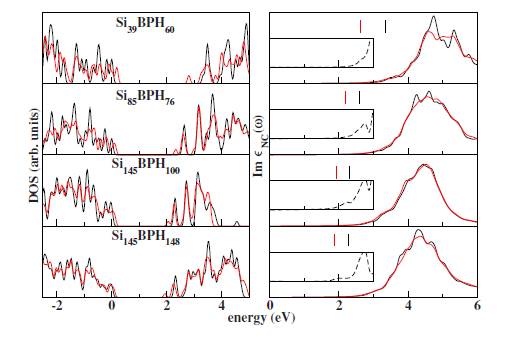
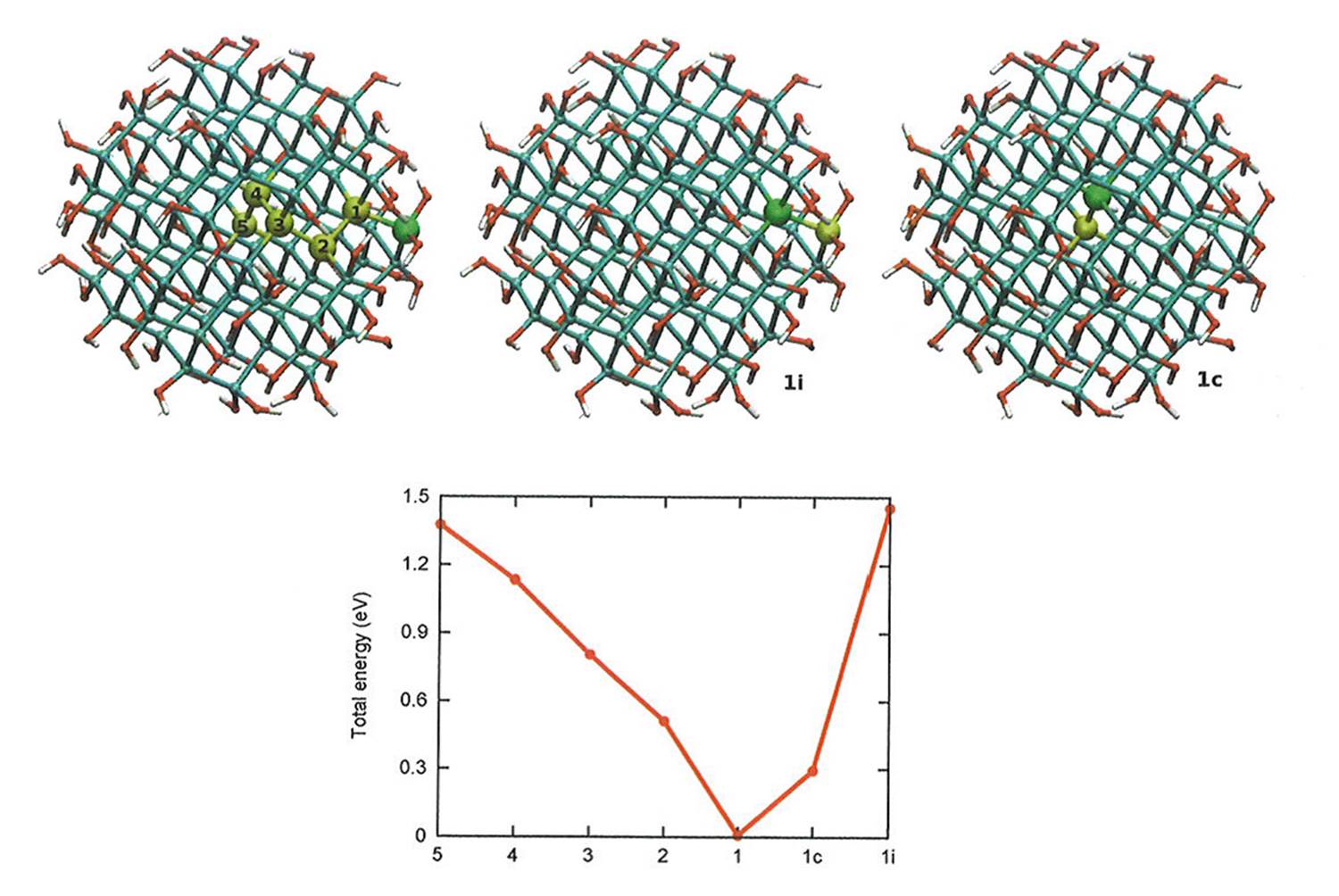
Alternatively, the P-B bond can be formed at the Si-NC center, fulfilling the ”minimum enegry costrain rule” of the single-doped Si-NC for the P dopant and forcing the B atom in the Si-NC core. Such configuration, named 1c, results more energetically favored than the 5, 4, 3, and 2 configurations, confirming the idea that the formation of the P-B bond prevails with respect to other parameters. However, the configuration of position 1 (P-B pair at the interface) remains most stable than the configuration of position 1c (P-B pair at the centre).
Due to the polar nature of the P-B bond, the above condition implies the formation of a static electric dipole radially directed and preferentially located at the Si-NC surface, which points toward the Si-NC center. Similar results have been obtained by Ni et al. [221]. The high stability of the dipole direction is evidenced by considering a configuration in which the codopants are switched, a B-P pair, named 1i (see Fig. 25). Quite interestingly, such configuration produces a total energy higher than all the other cases. The formation of stable dipoles at the Si-NCs surfaces radially directed inward the Si-NCs can provide an explanation of the production of stable colloidal codoped Si-NCs without surface functionalization processes [115, 116, 117, 242]. Moreover, since in the codoped case the minimum energy formation is found for the strong and stable P-B bond, also the intensity of the transition between HOMO (acceptor) and LUMO (donor) states in the codoped Si-NCs is affected by the impurity distance. Stronger transitions arise when the impurities are closer, whereas the intensity gets lower when the impurities are at larger distances, as shown by the calculated absorption spectra [92]. These results were confirmed by the experimental determination of strong PL intensities in colloidal and matrix-embedded codoped Si-NCs [117]. Similar theoretical outcomes have been obtained also for codoped Si-NWs [236, 237, 243, 244].
All these results found a confirmation in the atom probe tomography analysis of the B and the P distribution in codoped Si-NCs [129]. In Fig. 26 the proxigram analysis of codoped Si-NCs in BPSG matrix annealed at 1150 ∘C is reported. The distance at 0 nm represents the interface between the Si-NC and the matrix. Going to positive (negative) distance means moving towards the center of the Si-NC (inside the matrix). Clearly in the codoped Si-NCs the P concentration increases on going into the Si-NC, i.e. the P atom prefers to stay inside the Si region, whereas the B concentration does not show abrupt changes and reaches its maximum exactly at the Si-NC/matrix interface. Moreover a cluster analysis found that a large fraction of the B and P atoms present in the codoped samples were consumed to form B-P clusters in the Si-NCs, in good agreement with the theoretical results shown in Fig. 25.
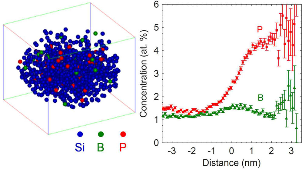
7 Conclusions
We presented a review of the recent activities concerning doping in silicon nanocrystals. Particular attention has been devoted to the theoretical outcomes that often complement the experimental analysis. After two decades of intense efforts, there is consensus about the possibility of incorporating boron and phosphorus as impurities in Si-NCs as small as 2 nm in diameter, where quantum confinement effects are particularly important. It is also clear that the incorporation of B and P in the Si-NCs does not depend only on the Si-NC size, but it is also influenced by the Si-NC interface and by the embedding medium. Theoretical and experimental outcomes pointed out that there are important differences between free-standing and matrix-embedded Si-NCs. A rapidly growing effort is devoted to the characterization of compensated codoped Si-NCs. Here we expect interesting results in the next years and an important impact in the development of future optoelectronic devices. For what concern doping in Si-NCs the most complicated issue regards the dopant electronic activation. Even if it has been demonstrated that this activation is possible, the efficiency is very low for both p- and n- impurities, with a clear preference for phosphorus with respect to boron. There is then space for new ideas aiming at the development of innovative strategies to realize doping in Si-NCs.
8 Acknowledgements
We are grateful to M. Amato, F. Iori and R. Guerra for useful discussions. The authors acknowledge the CINECA award under the ISCRA initiative, for the availability of high performance computing resources and support and the PRACE for awarding us access to resource Marconi and FERMI based in Italy at CINECA. Ivan Marri acknowledges support/funding from European Union H2020-EINFRA-2015-1 programme under grant agreement No. 676598 project ”MaX - materials at the exascale”.
9 References
References
- [1] L. C. Kimerling, Silicon Microphotonics, Appl. Surf. Sci. 159-160 (2000) 8–13.
- [2] S. Ossicini, L. Pavesi, F. Priolo, Light emitting silicon for microphotonics, Springer Tracts in Modern Physics 194 (2003) 1–282.
- [3] F. Priolo, F. Gregorkiewicz, M. Galli, T. F. Krauss, Silicon nanostructures for photonics and photovoltaics, Nature Nanotechnol. 1 (2014) 19–32.
- [4] M. Cazzanelli, F. Bianco, E. Borga, G. Pucker, M. Ghulinyan, E. Degoli, E. Luppi, V. Véniard, S. Ossicini, D. Modotto, S. Wabnitz, R. Pierobon, L. Pavesi, Second-harmonic generation in silicon waveguides strained by silicon nitride, Nature Mat. 11 (2012) 148–154.
- [5] L. T. Canham, Silicon quantum wire array fabrication by electrochemical and chemical dissolution of wafers, Appl. Phys. Lett. 57 (1990) 1046–1048.
- [6] H. Takagi, H. Ogawa, Y. Yamazaki, A. Ishikazi, T. Nakagiri, Quantum size effects on photoluminescence in ultrafine Si particles, Appl. Phys. Lett. 56 (1990) 2379–2381.
- [7] S. Ossicini, F. Bernardini, A. Fasolino, Gap opening in ultrathin Si layers: role of confined and interface states, Phys. Rev. Lett. 72 (1994) 1044–1047.
- [8] O. Bisi, S. Ossicini, L. Pavesi, Porous silicon, a quantum sponge structure for silicon based optoelectronics, Surface Sci. Rep. 38 (2000) 1–126.
- [9] I. Pelant, Optical gain in silicon nanocrystals: current status and perspectives, Phys. Status Solidi A 208 (2011) 625–630.
- [10] M. Fujii, ”Optical properties of intrinsic and shallow impurity-doped silicon nanocrystals”, in Silicon Nanocrystals ed. by L. Pavesi, and R. Turan, Wiley-Vch, Weinheim, 2010.
- [11] D. Jurbergs, E. Rogojina, L. Mangolini, U. Kortshagen, Silicon nanocrystals with ensemble quantum yields exceeding 60, Appl. Phys. Lett. 88 (2006) 233116.
- [12] L. Pavesi, L. Dal Negro, C. Mazzoleni, G. Franzó, F. Priolo, Optical gain in silicon nanocrystals, Nature 408 (2000) 440–444.
- [13] L. Khriachtchev, M. Räsänen, S. Novikov, J. Sinkonen, Optical gain in SiO/SiO2 lattice: Experimental evidence with nanosecond pulses, Appl. Phys. Lett. 79 (2001) 1249–1251.
- [14] M. H. Nayfeh, S. Rao, N. Barry, J. Therrien, G. Belomoin, A. Smith, S. Chaieb, Observation of laser oscillation in aggregates of ultrasmall silicon nanoparticles, Appl. Phys. Lett. 80 (2002) 121–123.
- [15] L. Dal Negro, M. Cazzanelli, L. Pavesi, S. Ossicini, D. Pacifici, G. Franzó, F. Priolo, F. Iacona, Dynamics of stimulated emission in silicon nanocrystals, Appl. Phys. Lett. 82 (2003) 4636–4638.
- [16] J. Ruan, P. M. Fauchet, L. Dal Negro, M. Cazzanelli, L. Pavesi, Stimulated emission in nanocrystalline silicon superlattices, Appl. Phys. Lett. 83 (2003) 5479–5481.
- [17] K. Luterová, K. Dohnalová, V. Ŝvrĉek, I. Pelant, J. P. Likforman, O. Crégut, P. Gilliot, B. Hönerlage, Optical gain in porous silicon grains embedded in sol-gel derived SiO2 matrix under femtosecond excitation, Appl. Phys. Lett. 84 (2004) 3280–3282.
- [18] K. Dohnalová, I. Pelant, K. Kusová, P. Gilliot, M. Gallart, O. Crégut, J. L. Rehspringer, B. Hönerlage, T. Ostatnický, S. Bakardjieva, Closely packed luminescent silicon nanocrystals in a distributed-feedback laser cavity, New J. Phys. 10 (2008) 063014.
- [19] E. Degoli, R. Guerra, F. Iori, R. Magri, I. Marri, O. Pulci, O. Bisi, S. Ossicini, Ab-initio calculations of luminescence and optical gain properties in silicon nanostructures, C. R. Phys. 10 (2009) 575–586.
- [20] L. Sirleto, M. A. Ferrara, T. Nikitin, S. Novikov, L. Khriachtchev, Giant Raman gain in silicon nanocrystals, Nature Comm. 3 (2012) 1220.
- [21] T. Nikitin, S. Novikov, L. Khriachtchev, Giant Raman gain in annealed silicon-rich silicon oxide films: Measurements at 785 nm, Appl. Phys. Lett. 103 (2013) 151110.
- [22] M. C. Beard, K. P. Knutsen, P. Yu, J. M. Luther, Q. Song, W. K. Metzger, R. J. Ellingson, A. J. Nozik, Multiple exciton generation in colloidal silicon nanocrystals, Nano Lett. 7 (2007) 2506–2512.
- [23] D. Timmermann, L. Izeddin, P. Stallinga, I. N. Yassevich, T. Gregorkiewicz, Space-separated quantum cutting with silicon nanocrystals for photovoltaic applications, Nature Photon. 2 (2008) 105–109.
- [24] M. T. Trinh, R. Limpens, W. D. A. M. de Boer, J. M. Schins, L. D. A. Siebbeles, T. Gregorkiewicz, Direct generation of multiple exciton in adjacent silicon nanocrystals revealed by induced absorption, Nature Photon. 6 (2012) 316–321.
- [25] M. Govoni, I. Marri, S. Ossicini, Auger recombination in Si and GaAs semiconductors: Ab initio results, Phys. Rev. B 84 (2011) 075215.
- [26] M. Govoni, I. Marri, S. Ossicini, Carrier multiplication between interacting nanocrystals for fostering silicon-based photovoltaics, Nature Photon. 6 (2012) 672–679.
- [27] I. Marri, M. Govoni, S. Ossicini, Red-shifted carrier multiplication energy threshold and exciton recycling mechanisms in strongly interacting silicon nanocrystals, J. Am. Chem. Soc. 136 (2014) 13257–13266.
- [28] I. Marri, M. Govoni, S. Ossicini, Carrier multiplication in silicon nanocrystals: ab initio results, Beilstein J. Nanotech. 6 (2015) 343–352.
- [29] I. Marri, M. Govoni, S. Ossicini, First-principle calculations of electronic coupling effects in silicon nanocrystals: Influence on near band-edge states and on carrier multiplication processes, Solar Energy Materials & Solar Cells 145 (2016) 162–169.
- [30] K. Dohnalová, T. Gregorkiewicz, K. Kûsová, Silicon quantum dots: surface matters, J. Phys.: Condens. Matter 26 (2014) 173201.
- [31] D. V. Talapin, J. S. Lee, M. V. Kovalenko, E. V. Shevchenko, Prospects of colloidal nanocrystals for electronic and optoelectronic applications, Chem. Rev. 110 (2010) 389–458.
- [32] A. Gupta, A. S. G. Khalil, M. Offer, M. Geller, M. Winterer, A. Lorke, H. Wiggers, Synthesis and ink-jet printing of highly luminescing silicon nanoparticles for printable electronics, Nanotechnol. 11 (2011) 5028–5033.
- [33] N. Daldosso, L. Pavesi, Nanosilicon photonics, Laser & Photon. Rev. 3 (2009) 508–534.
- [34] L. Kriachtchev, S. Ossicini, F. Iacona, F. Gourbilleau, Silicon nanoscale materials: From theoretical simulations to photonic applications, Int. J. Photoen. (2012) 872576.
- [35] K. Imakita, M. Ito, M. Fujii, S. Hayagy, Nonlinear optical properties of phosphorus-doped Si nanocrystals embedded in phosphosilicate glass thin films, Optics Express 17 (2009) 7368–7376.
- [36] Z. Bisadi, M. Mancinelli, S. Manna, S. Tondini, M. Bernard, A. Samusenko, M. Ghulinyan, G. Fontana, P. Bettotti, F. Ramiro-Manzano, G. Pucker, L. Pavesi, Silicon nanocrystals for nonlinear optics and secure communications, Phys. Status Solidi A 212 (2015) 2659–2671.
- [37] S. V. Makarov, M. I. Petrov, U. Zywietz, V. A. Milichko, D. A. Zuev, N. Lopanitsyna, A. Kuksin, I. Mukhin, G. Zograf, E. Ubyivovk, D. Smirnova, S. Starikov, B. N. Chichkov, Y. S. Kivshar, Efficient second-harmonic generation in nanocrystalline silicon nanoparticle, Nanolett. (2017) 2017.
- [38] M. A. Green, Third-generation photovoltaics: ultra-high conversion efficiency at low cost, Prog. Photovolt: Res. Appl. 9 (2001) 123–135.
- [39] A. J. Nozik, Nanosciences and nanostructures for photovoltaics and solar fuels, Nano Lett. 10 (2010) 2735.
- [40] G. Conibeer, M. A. Green, D. König, I. Perez-Würfl, S. Huang, X. Xao, D. Di, L. Shi, S. Shrestha, B. Putheen-Veettil, Y. So, B. Zhang, Z. Wan, Silicon quantum dots based solar cells: addressing the issue of doping, voltage and current transport, Prog. Photovolt: Res. Appl. 19 (2011) 813–824.
- [41] L. Mangolini, Synthesis, properties, and applications of silicon nanocrystals, J. Vac. Sci. Technol. B 31 (2013) 020801.
- [42] P. Löper, M. Canino, J. López-Vidrier, M. Schnabel, F. Schindler, F. Heinz, A. Witzky, M. Bellettato, M. Allegrezza, D. Hiller, A. Hartel, S. Gutsch, S. Hérnandez, R. Guerra, S. Ossicini, B. Garrido, S. Janz, M. Zacharias, Silicon nanocrystals from high-temperature annealing: Characterization on device level, Phys. Status Solidi A 210 (2013) 669–675.
- [43] C. Summonte, M. Allegrezza, M. Bellettato, F. Liscio, M. Canino, A. Desalvo, J. López-Vidrier, S. Hernández, L. Lopéz-Conesa, S. Estradé, F. Peiró, B. Garrido, P. Löper, M. Schnabel, S. Janz, R. Guerra, S. Ossicini, Silicon nanocrystals in carbide matrix, Solar Energy Materials & Solar Cells 128 (2014) 138–149.
- [44] M. S. Dresselhaus, C. Gang, Y. T. Ming, Y. Ronggui, L. Hohyun, W. Dezhi, R. Zhifeng, J. P. Fleurial, G. Pawan, New directions for low-dimensional thermoelectric materials, Adv. Mater. 19 (2007) 1043–1053.
- [45] T. Claudio, N. Stein, D. G. Stroppa, B. Klobes, M. M. Koz, P. Kudejova, N. Petermann, H. Wiggers, G. Schierning, R. P. Hermann, Nanocrystalline silicon: lattice dynamics and enhanced thermoelectric properties, Phys. Chem. Chem. Phys. 16 (2014) 25701–25709.
- [46] N. O’Farrell, A. Houlton, B. R. Horrocks, Silicon nanoparticles: applications in cell biology and medicine, J. Nanomed. 1 (2006) 451–472.
- [47] F. Erogbobo, K. T. Yong, I. Roy, G. X. Xu, P. N. Prasad, M. T. Swihart, Biocompatible luminescent silicon quantum dots for imaging of cancer cells, ACS Nano 2 (2008) 873–878.
- [48] X. Cheng, S. B. Lowe, P. J. Reece, J. J. Gooding, Colloidal silicon quantum dots: from preparation to the modification of self assembled monolayers (sams) for bio-applications, Chem. Soc. Rev. 43 (2014) 2680–2700.
- [49] L. Ostrovska, A. Broz, A. Fucikova, T. Belinova, H. Sugimoto, T. Kanno, M. Fujii, J. Valenta, M. Hubalek Kabalcova, The impact of doped silicon quantum dots on human osteoblasts, RSC Advances 6 (2016) 63403–63413.
- [50] B. F. P. McVey, S. Prabakar, J. J. Goodig, R. D. Tilley, Solution, synthesis, surface passivation, optical properties, biomedical applications, and cytotoxicity of silicon and germanium nanocrystals, ChemPlusChem 82 (2017) 60–73.
- [51] Y. Kanemitsu, Mechanism of visible photoluminescence from oxidized silicon and germanium nanocrystallites, Thin Solid Films 276 (1996) 44–46.
- [52] L. Dorigoni, O. Bisi, F. Bernardini, S. Ossicini, Electron states and luminescence transition in porous silicon, Phys. Rev. B 53 (1996) 4557–4564.
- [53] A. S. Moskalenko, J. Berakdar, A. A. Prokofiev, Y. N. Yassievich, Single-particle states in spherical Si/SiO2 quantum dots, Phys. Rev. B 76 (2007) 085427.
- [54] M. Sykora, L. Mangolini, R. D. Schaller, U. Kortshagen, D. Jurbergs, V. I. Klimov, Size-dependent intrinsic radiative decay rates of silicon nanocrystals at large confinement energies, Phys. Rev. Lett. 100 (2008) 067401.
- [55] G. Allan, C. Delerue, M. Lannoo, Nature of luminescent surface states of semiconductor nanocrystallites, Phys. Rev. Lett. 76 (1996) 2961–2964.
- [56] M. V. Wolkin, J. Jorne, J. M. Fauchet, G. Allan, C. Delerue, Electronic states and luminescence in porous silicon quantum dots: The role of oxygen, Phys. Rev. Lett. 82 (1999) 000197.
- [57] T. Shimitsu-Iwayama, T. Hama, D. E. Hole, I. W. Boyd, Characteristic photoluminescence properties of Si nanocrystals in SiO2 fabricated by ion implantation and annealing, Solid-State Electronics 45 (2001) 1487–1494.
- [58] J. Martin, F. Chicos, F. Huisken, C. von Borczyskowski, Electron-phonon coupling and localization of excitons in single silicon nanocrystals, Nano Lett. 8 (2008) 656–670.
- [59] M. Dovrat, Y. Shalibo, N. Arad, I. Popov, S. T. Lee, A. Sa’ar, Fine structure and selection rules for excitonic transitions in silicon nanostructures, Phys. Rev. B 79 (2009) 125306.
- [60] L. Koponen, L. O. Tunturivuori, M. J. Puska, R. M. Nieminen, Effect of the surrounding oxide on the photoabsorption spectra of Si nanocrystals, Phys. Rev. B 79 (2009) 235332.
- [61] A. Filonov, S. Ossicini, F. Bassani, F. Arnaud D’Avitaya, Effect of oxygen on the optical properties of small silicon pyramidal clusters, Phys. Rev. B 65 (2002) 195317.
- [62] M. Luppi, S. Ossicini, Multiple Si=O bonds at silicon clusters surface, J. Appl. Phys. 94 (2003) 2130–2132.
- [63] N. Daldosso, M. Luppi, S. Ossicini, E. Degoli, R. Magri, G. Dalba, D. Fornasini, R. Grisenti, F. Rocca, L. Pavesi, S. Boninelli, F. Priolo, C. Spinella, F. Iacona, Role of the interface region on the optoelectronic properties of silicon nanocrystals embedded in SiO2, Phys. Rev. B 68 (2003) 085327.
- [64] Z. Zhou, L. Brus, R. Friesner, Electronic structure and luminescence of 1.1- and 1.4-nm silicon nanocrystals: Oxide shell versus hydrogen passivation, Nano Lett. 3 (2003) 163–167.
- [65] S. Ossicini, O. Bisi, E. Degoli, I. Marri, F. Iori, E. Luppi, R. Magri, R. Poli, G. Cantele, D. Ninno, F. Trani, M. Marsili, O. Pulci, V. Olevano, M. Gatti, K. Gaal-Nagy, A. Incze, G. Onida, First principle study of silicon nanocrystals: Structural and electronic properties, absorption, emission and doping, J. Nanosci, Nanotech. 8 (2008) 479–492.
- [66] X. J. Hao, A. P. Podhorodecki, Y. S. Shen, G. Zatryb, J. Misiewicz, M. A. Green, Effects of Si-rich oxide layer stoichiometry on the structural and optical properties of Si QD/SiO2 multilayer films, Nanotechnology 20 (2009) 485703.
- [67] F. Gourbilleau, C. Ternon, D. Maestre, O. Palais, C. Dofour, Silicon-rich SiO2/SiO2 multilayers: A promising material for the third generation of solar cell, J. Appl. Phys. 106 (2009) 013501.
- [68] R. Guerra, I. Marri, R. Magri, L. Martin-Samos, O. Pulci, E. Degoli, S. Ossicini, Silicon nanocrystallites in a SiO2 matrix: Role of disorder and size, Phys. Rev. B 79 (2009) 155320.
- [69] R. Guerra, E. Degoli, S. Ossicini, Size, oxydation and strain in Si/SiO2 nanocrystals, Phys. Rev. B 80 (2009) 155332.
- [70] O. Pulci, E. Degoli, F. Iori, M. Marsili, M. Palummo, R. Del Sole, S. Ossicini, Electronic and optical properties of silicon and germanium nanocrystals: an ab-initio study, Superlattices and Microstructures 47 (2010) 178–181.
- [71] R. Guerra, S. Ossicini, High luminescence in small Si/SiO2 nanocrystals, Phys. Rev. B 81 (2010) 245307.
- [72] R. Guerra, E. Degoli, M. Marsili, O. Pulci, S. Ossicini, Local field and disorder effects in free-standing and embedded Si nanocrystallites, Phys. Stat. Solidi B 247 (2010) 2113–2117.
- [73] R. Guerra, M. Marsili, O. Pulci, S. Ossicini, Local-field effects in silicon nanoclusters, Phys. Rev. B 84 (2011) 075342.
- [74] G. Seguini, C. Castro, S. Schamm-Chardon, G. BenAssayag, P. Pellegrino, M. Perego, Scaling size of the interplay between quantum confinement and surface related effects in nanostructured silicon, Appl. Phys. Lett. 103 (2013) 023103.
- [75] A. G. Cullis, L. T. Canham, P. D. J. Calcott, The strutural and luminescence properties of porous silicon, J. Appl. Phys. 82 (1997) 909–965.
- [76] G. Polisski, D. Kovalev, G. Dollinger, T. Sulima, F. Koch, Boron in mesoporous Si-where have all the carrier gone?, Physica B 273-274 (1999) 951–954.
- [77] M. Fujii, Y. Yamaguchi, Y. Takase, K. Ninomiya, S. Hayashy, Photoluminescence from impurity codoped and compensated Si nanocrystals, Appl. Phys. Lett. 87 (2005) 211919.
- [78] B. L. Oliva-Chatelain, T. M. Ticich, A. R. Barron, Doping silicon nanocrystals and quantum dots, Nanoscale 8 (2016) 1733–1745.
- [79] E. Arduca, M. Perego, Doping of silicon nanocrystals, Materials Science in Semiconductor Processing 62 (2017) 156–170.
- [80] D. V. Melnikov, J. R. Chelikowsky, Quantum confinement in phosphorus-doped silicon nanocrystals, Phys. Rev. Lett. 92 (2004) 046802.
- [81] G. Cantele, E. Degoli, E. Luppi, R. Magri, D. Ninno, G. Jadonisi, S. Ossicini, First principles study of n- and p-doped silicon nanoclusters, Phys. Rev. B 72 (2005) 113303.
- [82] S. Ossicini, E. Degoli, F. Iori, E. Luppi, R. Magri, G. Cantele, F. Trani, D. Ninno, Simultaneously B- and P- doped silicon nanoclusters: formation energies and electronic properties, Appl. Phys Lett. 87 (2005) 1–3.
- [83] G. M. Dalpian, J. R. Chelikowsky, Self-purification in semiconductor nanocrystals, Phys. Rev. Lett. 96 (2006) 226802.
- [84] T. L. Chan, M. L. Tiago, E. Kaxiras, J. R. Chelikowsky, Size limits on doping into silicon nanocrystals, Nano Lett 8 (2008) 596–600.
- [85] D. J. Norris, A. L. Efros, S. C. Erwin, Doped nanocrystals, Science 319 (2008) 1766–1779.
- [86] J. Li, S. H. Wei, S. S. Li, J. B. Xia, Origin of the doping bottleneck in semiconductors quantum dots: a first principle study, Phys. Rev. B 77 (2008) 113304.
- [87] J. R. Chelikowsky, M. M. G. Alemany, T. L. Chan, G. M. Dalpian, Computational studies of doped nanostructures, Rep. Prog. Phys. 74 (2011) 046501.
- [88] G. M. Credo, M. D. Mason, S. K. Buratto, External quantum efficiency of single porous silicon nanoparticles, Appl. Phys. Lett. 74 (1999) 1978–1981.
- [89] R. N. Pereira, A. J. Almeida, Doped semiconductor nanoparticles synhesized in gas-phase plasmas, J. Phys. D: Appl. Phys. 48 (2015) 314005.
- [90] Z. Ni, X. Pi, M. Ali, S. Zhou, T. Nozaki, D. Yang, Freestanding doped silicon nanocrystals synhesized by plasma, J. Phys. D: Appl. Phys. 48 (2015) 314006.
- [91] G. Onida, L. Reining, A. Rubio, Electronic excitations: density-functional versus many-body Green’s-function approaches, Rev. Mod. Phys. 74 (2) (2002) 601–659.
- [92] F. Iori, E. Degoli, R. Magri, I. Marri, G. Cantele, D. Ninno, F. Trani, O. Pulci, S. Ossicini, Engineering silicon nanocrystals: theoretical study of the effect of codoping with boron and phosphorus, Phys. Rev. B 76 (2007) 085302.
- [93] M. Luppi, S. Ossicini, Ab-initio study on oxidized silicon clusters and on silicon nanocrystals embedded in SiO2, Phys. Rev. B 71 (2005) 035340.
- [94] R. Guerra, I. Marri, R. Magri, L. Martin-Samos, O. Pulci, E. Degoli, S. Ossicini, Optical properties of silicon nanocrystallites in SiO2 matrix: crystalline vs. amorphous case, Superl. Microstr. 46 (2009) 246–252.
- [95] M. Ehbrecht, F. Huisken, Gas-phase characterization of silicon nanoclusters produced by laser pyrolysis of silane, Phys. Rev. B 59 (1999) 2975–2985.
- [96] W. L. Wilson, P. F. Szajowski, L. E. Brus, Quantum confinement in size-selected, surface-oxidized silicon nanocrystals., Science 262 (1993) 1242–1244.
- [97] A. A. Onischuk, V. P. Strunin, M. A. Ushakova, V. N. Panfilov, On the pathways of aerosol formation by thermal decomposition of silane, J. Aerosol. Sci 28 (1997) 207–222.
- [98] M. L. Ostraat, J. W. De Blauwe, M. L. Green, L. D. Bell, M. L. Brongersma, J. Casperson, R. C. Flagan, H. A. Atwater, Synthesis and characterization of aerosol silicon nanocrystal nonvolatile floating-gate memory devices, Appl. Phys. Lett. 79 (2001) 433–435.
- [99] E. Werwa, A. A. Seraphin, L. A. Chiu, C. X. Zhou, K. D. Kolenbrander, Synthesis and processing of silicon nanocrystallites using a pulsed laser ablation supersonic expansion method, Appl. Phys. Lett. 64 (1994) 1821–1823.
- [100] L. Mangolini, E. Thimsen, U. Kortshagen, High-yield plasma synthesis of luminescent silicon nanocrystals, Nano Lett. 5 (2005) 655–659.
- [101] J. D. Holmes, K. J. Ziegler, R. C. Doty, L. E. Pell, K. P. Johnston, B. A. Korgel, Highly luminescent silicon nanocrystals with discrete optical transitions, J. Am. Chem. Soc. 123 (2001) 3743–3748.
- [102] C. M. Hessel, D. Reid, M. G. Panthani, M. R. Rasch, B. W. Goodfellow, J. W. Wei, H. Fujii, V. Akhavan, B. A. Korgel, Synthesis of ligand-stabilized silicon nanocrystals with size-dependent photoluminescence spanning visible to near-infrared wavelengths, Chem Mat. 24 (2012) 393–401.
- [103] J. Knipping, H. Woggers, B. Ellinghaus, P. Roth, D. Konjhodzic, C. Meier, Synthesis of high purity silicon nanoparticles in a low pressure microwave reactor, J. Nanosci. Nanotechnol. 4 (1039) 1039–2004.
- [104] J. G. C. Veinot, Synthesis, surface functionalization, and properties of freestanding silicon nanocrystals, Chem. Commun. (2006) 4160–4168.
- [105] U. R. Kortshagen, R. Mohan Snakaran, R. N. Pereira, S. L. Girshick, J. J. Wu, E. R. Aydil, Nonthermal plasma synthesis of nanocrystals: Fundamental principles, materials, and applications, Chem. Rev. 116 (2016) 11061–11127.
- [106] Y. Yin, P. Alivisatos, Colloidal nanocrystal synthesis and the organic-inorganic interface, Nature 437 (2005) 664–670.
- [107] R. N. Pereira, D. J. Rowe, R. J. Anthony, U. Kortshagen, Freestanding siicon nanocrystals with extremely low defect content, Phys Rev. B 86 (2012) 085449.
- [108] X. D. Pi, R. W. Liptak, J. D. Nowak, N. P. Wells, C. B. Carter, S. A. Campbell, U. Kortshagen, Air-stable full-visible-spectrum emission from silicon nanocrystals synthesized by an all-gas-phase plasma approach, Nanotechnology 19 (2008) 245603.
- [109] M. Dasog, G. B. De Los Reyes, L. V. Titova, F. Hegmann, J. G. C. Veinot, Size vs surface: tuning the photoluminescence spectra of freestanding silicon nanocrystals across the visible spectrum via surface groups, ACS Nano 8 (2014) 9636–9648.
- [110] X. D. Pi, R. Gresback, R. W. Liptak, S. A. Campbell, U. Kortshagen, Doping efficiency, dopant location, and oxidation of Si nanocrystals, Appl. Phys. Lett. 92 (2008) 123102.
- [111] R. K. Baldwin, J. Zou, K. A. Pettigrew, G. J. Yeagle, R. D. Britt, S. M. Kauzlarich, The preparation of a phosphorus doped silicon film from phosphorus containing silicon nanoparticles, Chem. Commun. 6 (2006) 658–660.
- [112] K. Someno, K. Usami, T. Kodera, Y. Kawano, M. Hatano, S. Oda, Photoluminescence of nanocrystaline silicon quantum dots with various sizes and various phosphorus doping concentrations prepared by very high frequency plasma, J. Appl. Phys. 51 (2012) 115202.
- [113] Y. Ma, X. Chen, X. Pi, D. Yang, Lightly boron and phosphorus co-doped silicon nanocrystals, J. Nanopart. Res. 14 (2012) 802.
- [114] H. Sugimoto, M. Fujii, M. Fukuda, K. Imakita, S. Hayashi, Acceptor-related low-energy photoluminescence from boron-doped Si nanocrystals, J. Appl. Phys. 110 (2011) 063528.
- [115] H. Sugimoto, M. Fujii, K. Imakita, S. Hayashi, K. Akamatsu, All-inorganic near-infrared luminescent colloidal silicon nanocrystals: high dispersibility in polar liquid by phosphorus and boron codoping, J. Phys. Chem C 116 (2012) 19769–19774.
- [116] H. Sugimoto, M. Fujii, K. Imakita, S. Hayashi, K. Akamatsu, Phosphorus and boron codoped silicon nanocrystals with inorganic atomic ligands, J. Phys. Chem. C 117 (2013) 6807–6813.
- [117] H. Sugimoto, M. Fujii, K. Imakita, S. Hayashi, K. Akamatsu, Codoping n- and p-type impurities in colloidal silicon nanocrystals: controlling visible photoluminescnece from below bulk band gap to visible photoluminescence, J. Phys. Chem. C 117 (2013) 11850–11857.
- [118] M. Fujii, H. Sugimoto, M. Hasegawa, K. Imakita, Silicon nanocrystals with high boron and phosphorus concentration hydrophilic shell-Raman scattering and X-ray photoelectron spectroscopic studies, J. Appl. Phys. 115 (2014) 084301.
- [119] T. Kanno, H. Sugimoto, A. Fucikova, J. Valenta, M. Fujii, Single-dot spectroscopy of boron and phosphorus codoped silicon quantum dots, J. Appl. Phys. 12 (2016) 164307.
- [120] A. J. Almeida, H. Sugimoto, M. Fujii, S. M. Brandt, M. Stutzmann, R. N. Pereira, Doping efficiency and confinement of donors in embedded and free standing Si nanocrystals, Phys. Rev. B 93 (2016) 115425.
- [121] N. Salivati, N. Shuall, J. M. McCrate, J. G. Ekerdt, Effect of subsurface boron on photoluminescence from silicon nanocrystals, Surf. Sci. 605 (2011) 799–801.
- [122] A. Zhou, Y. Ding, X. Pi, T. Nozaki, Doped silicon nanocrystals from organic dopant precursos by a SiCl4-based high-frequency nonthermal plasma, Appl. Phys. Lett. 105 (2014) 2012–2017.
- [123] S. Zhou, X. Pi, Z. Ni, Q. Luan, Y. Jiang, C. Jin, T. Nozaki, D. Yang, Boron- and phosphorus-hyperdoped silicon nanocrystals, Part. Part. Syst. Charact. 32 (2015) 213–221.
- [124] N. J. Kramer, K. S. Schramke, U. R. Kortshagen, Plasmonic properties of silicon nanocrystals doped with boron and phosphorus, Nano Lett. 15 (2015) 5597–5603.
- [125] S. Zhou, X. Pi, Z. Ni, Y. Ding, Y. Jiang, C. Jin, C. Delerue, D. Yang, T. Nozaki, Comparative study on the localized surface plasmon resonance of boron and phosphorous doped silicon nanocrystals, ACS Nano 9 (2015) 378–386.
- [126] Z. Ni, X. Pi, S. Zhou, T. Nozaki, B. Grandidier, Size-dependent structures and optical absorption of boron-hyperdoped silicon nanocrystals, Adv. Optical Mater. 4 (2016) 700–707.
- [127] S. Zhou, Z. Ni, Y. Ding, M. Sugaya, X. Pi, T. Nozaki, Ligand-free, colloidal and plasmonic silicon nanocrystals heavily doped with boron, ACS Photonics 3 (2016) 415–422.
- [128] J. Xu, J. Xu, P. Lu, D. Shan, W. Li, K. Chen, Charge transfer of single laser crystallised intrinsic and phosporus-doped silicon-nanocrystals visualised by Kelvin probe microscope, J. Appl. Phys. 116 (2014) 134309.
- [129] K. Nomoto, H. Sugimoto, A. Breen, A. V. Ceguerra, T. Kanno, S. P. Ringer, I. Perez-Würfl, G. Conibeer, M. Fujii, Atom probe tomography analysis of boron and/or phosphorus distribution in doped silicon nanocrystals, J. Phys. Chem. C 120 (2016) 17845–17852.
- [130] R. N. Pereira, A. R. Stegner, T. Andlauer, K. Klein, H. Wiggers, S. M. Brandt, M. Stutzmann, Dielectric screening versus quantum confinement of phosphorus donors in silicon nanocrystals investigated by magnetic resonance, Phys. Rev. B 79 (2009) 161304(R).
- [131] Y. Nakamine, N. Inaba, K. Kodera, T ad Uchida, A. R. Pereira, R N amd Stegner, M. S. Brandt, M. Stutzmann, S. Oda, Size reduction and phosphorus doping of silicon nanocrystals prepared by a very high frequency plasma deposition system, Jpn. J. Appl. Phys. 50 (2011) 2–7.
- [132] R. N. Pereira, A. R. Stegner, K. Klein, R. Lechner, R. Dietmueller, H. Wiggers, M. S. Brandt, M. Stutzmann, Electronic transport through Si nanocrystal films: Spin-dependent conductivity studies, Physica E 401 (2007) 527–530.
- [133] R. Lechner, A. R. Stegner, R. N. Pereira, R. Dietmueller, M. S. Brandt, A. Ebbers, M. Trocha, H. Wiggers, M. Stutzmann, Electronic properties of doped silicon nanocrystals films, J. Appl. Phys. 104 (2008) 053701.
- [134] A. R. Stegner, R. N. Pereira, K. Klein, R. Lechner, D. R, S. Brandt, M. Stutzmann, H. Wiggers, Electron transport in phosphorus-doped silicon nanocrystals networks, Phys. Rev. Lett. 100 (2008) 026803.
- [135] A. R. Stegner, R. N. Pereira, R. Lechner, K. Klein, H. Wiggers, M. Stutzmann, M. S. Brandt, Doping efficiency in freestanding silicon nanocrystals from the gas phase: phosphorus incorporation and defect-induced compensation, Phys. Rev. B 80 (2009) 165326.
- [136] R. Gresback, N. J. Kramer, Y. Ding, T. Chen, U. R. Kortshagen, T. Nozaki, Controled doping of silicon nanocrystals investigated by solution-processes field effect transistors, ACS Nano 8 (2014) 5650–5656.
- [137] D. J. Rowe, J. S. Jeong, K. A. Mkhoyan, U. R. Kortshagen, Phosphorus-doped silicon nanocrystals exhibiting mid infrared localized plasmon resonance, Nano Lett. 13 (2013) 1317–1322.
- [138] E. Degoli, S. Ossicini, Engineering quantum confined silicon nanostructures: Ab-initio study of the structural, electronic and optical properties, Adv. Quant. Chem. 58 (2009) 203–279.
- [139] Z. Zhou, A. R. Friesner, L. Brus, Electronic structure of 1 to 2 nm diameter silicon core/shell nanocrystals: Surface chemistry, optical spectra, charge transfer, and doping, J. Am. Chem. Soc. 125 (2003) 15559–15607.
- [140] E. Degoli, G. Cantele, E. Luppi, R. Magri, D. Ninno, O. Bisi, S. Ossicini, Ab-initio structural and electronic properties of hydrogenated silicon nanoclusters in their ground and excited state, Phys. Rev. B 69 (2004) 155411.
- [141] L. E. Ramos, J. Furthmüller, F. Bechstedt, Quantum confinement in Si- and Ge- capped nanocrystallites, Phys. Rev. B 72 (2005) 045351.
- [142] L. E. Ramos, E. Degoli, G. Cantele, S. Ossicini, D. Ninno, J. Furthmüller, F. Bechstedt, Structural features and electronic properties of group-III, group-IV and group-V-doped Si nanocrystallites, J. Phys.: Condens. Matter 19 (2007) 466211.
- [143] Z. Zhou, M. L. Steigerwald, A. R. Friesner, L. Brus, M. S. Hybertsen, Structural and chemical trends in doped silicon nanocrystals: first-principles calculations, Phys. Rev. B 71 (2005) 245308.
- [144] J. Zeng, H. Yu, A first-principle study of B- and P-doped silicon quantum dots, J. Nanomater. (2012) 147169.
- [145] S. Ossicini, F. Iori, E. Degoli, E. Luppi, R. Magri, G. Cantele, F. Trani, D. Ninno, Understanding doping in silicon nanostructures, IEEE J. Sel. Top. Quantum El. 12 (2006) 1585–1591.
- [146] S. Ossicini, E. Degoli, F. Iori, O. Pulci, G. Cantele, R. Magri, O. Bisi, F. Trani, D. Ninno, Doping in silicon nanocrystals, Surface Sci. 601 (2007) 2724–2729.
- [147] R. Magri, E. Degoli, F. Iori, E. Luppi, O. Pulci, S. Ossicini, G. Cantele, F. Trani, D. Ninno, Role of surface passivation and doping in silicon nanocrystals, J, Comput. Meth. Sci. Eng. 7 (2007) 219–232.
- [148] G. M. Dalpian, J. R. Chelikowsky, Dalpian and Chelikowksy Reply, Phys. Rev. Lett. 100 (2008) 179703.
- [149] J. Ma, S. H. Wei, Chemical trends and formation energies of the group-III and the group-V dopants in Si quantum dots, Phys. Rev B 87 (2013) 115318.
- [150] Q. Xu, J. W. Luo, S. S. Li, J. B. Xia, J. Li, S. H. Wei, Chemical trends of defect formation in Si quantum dots: the case of group-III and group-V dopants, Phys. Rev. B 75 (2007) 235304.
- [151] T. L. Chan, S. B. Zhang, J. R. Chelikowsky, An effective one-particle theory for formation energies in doping Si nanostructures, Appl. Phys. Lett. 98 (2011) 133116.
- [152] T. Z. Chan, H. Kwak, J. H. Eom, Z. S. B, J. R. Chelikowsky, Self-purification in Si nanocrystals: an energetic study, Phys. Rev. B 82 (2010) 115421.
- [153] M. Perego, C. Bonafos, M. Fanciulli, Phosphorus doping of ultra-small silicon nanocrystals, Nanotechnology 21 (2010) 025602.
- [154] M. Perego, G. Seguini, Fanciulli, ToF-SIMS study of phosphorus diffusion in low-dimensional silicon structures, Surf. Interface Anal. 45 (2013) 386–389.
- [155] K. Nomoto, S. Gutsch, A. V. Ceguerra, A. Breen, H. Sugimoto, M. Fujii, I. Perez-Würfl, S. P. Ringer, G. Conibeer, Atom probe tomography of phosphorus- and boron- doped silicon nanocrystals with various composition of silicon rich oxide, MRS Communications 6 (2016) 283–288.
- [156] K. Nomoto, D. Hiller, S. Gutsch, A. V. Ceguerra, B. A, M. Zacharias, G. Conibeer, P.-W. I, S. P. Ringer, Atom probe tomography of size controlled phosphorus doped silicon nanocrystals, Phys. Status Solidi RRL 11 (2017) 1600376.
- [157] J. H. Eom, T. L. Chan, J. R. Chelikowsky, Vacancies and B doping in Si nanocrystals, Solid State Commun. 150 (201) 130–132.
- [158] J. Ma, S. Wei, N. R. Neale, A. J. Nozik, Effect of surface passivation on dopant distribution in Si quantum dots: the case of B and P doping, Appl. Phys. Lett. 98 (2011) 173103.
- [159] X. Pi, X. Chen, D. Yang, First-principle study of 2.2 nm silicon nanocrystals doped with boron, J. Phys. Chem. C 115 (2011) 9388–9843.
- [160] X. Chen, X. Pi, D. Yang, Critical role of dopant location for P-doped Si nanocrystals, J. Phys. Chem. C 115 (2011) 661–666.
- [161] X. Pi, Doping silicon-nanocrystals with boron and phosphorus, J. Nanomater (2012) 912903.
- [162] A. Carvalho, M. J. Rayson, P. R. Briddon, Effect of oxidation on the doping of silicon nanocrystals with group III and group V elements, J. Phys. Chem. C 116 (2012) 8243–8250.
- [163] A. Carvalho, B. Celikkol, J. Coutinho, P. Briddon, Surface-phosphorus interaction in Si-nanocrystals, J. Phys. Conf. Ser. 281 (2011) 012027.
- [164] A. Carvalho, S. Öberg, M. Barroso, M. J. Rayson, P. Briddon, P-doping of Si nanoparticles: the effect of oxidation, Phys. Status Solidi A 209 (2012) 1847–1850.
- [165] A. Carvalho, S. Öberg, M. Barroso, M. J. Rayson, P. Briddon, Boron doped Si nanoparticles: the effect of oxidation, Phys. Status Solidi B 250 (2013) 1799–1803.
- [166] R. Guerra, S. Ossicini, Preferential positioning of dopants and codopants in embedded and freestanding Si nanocrystals, J. Am. Chem. Soc. 36 (2014) 4404–4409.
- [167] M. Lannoo, C. Delerue, G. Allan, Screening in semiconductor nanocrystallites and its consequences for porous silicon, Phys. Rev. Lett. 74 (1995) 3415–3418.
- [168] S. Öǧüt, J. R. Chelikowsky, S. G. Louie, Quantum confinement and optical gaps in Si nanocrystals, Phys. Rev. Lett. 79 (1997) 1770–1773.
- [169] D. Ninno, F. Trani, G. Cantele, K. Hameuuw, G. Iadonisi, E. Degoli, S. Ossicini, Thomas-Fermi model of electronic screening in semiconductor nanocrystals, Europhys. Lett. 74 (2006) 519–525.
- [170] D. Ninno, F. Trani, G. Cantele, G. Iadonisi, K. Hameuuw, E. Degoli, S. Ossicini, Screening in semiconductor nanocrystals: Ab-initio results and Thomas-Fermi theory, Phys. Rev. B 73 (2006) 245430.
- [171] F. Trani, D. Ninno, G. Cantele, E. Degoli, S. Ossicini, Impurity screening in silicon nanocrystals, Physica E 41 (2009) 966–968.
- [172] M. G. Mavros, D. A. Micha, D. S. Kilin, Optical properties of doped silicon quantum dots with crystalline and amorphous structure, J. Chem. Phys. C 115 (2011) 19527–19532.
- [173] X. Pi, Z. Ni, D. Yang, C. Delerue, Ab-initio study on the effect of structural relaxation on the electronic and optical propertieis of P-doped silicon nanocrystals, J. Appl. Phys. 116 (2014) 194304.
- [174] M. Fujii, A. Mimura, S. Hayashi, Y. Yamamoto, K. Murakami, Hyperfine structure of the electron spin resonance of phosphorus-doped Si nanocrystals, Phys. Rev. Lett. 89 (2002) 206805.
- [175] K. Sumida, K. Ninomiya, M. Fujii, K. Fujio, S. Hayashi, Electron spin-resonance studies of conduction electrons in phosphorus-doped silicon nanocrystals, J. Appl. Phys. 101 (2007) 033504.
- [176] K. H. Khoo, J. R. Chelikowsky, First-principles study of vibrational modes and Raman spectra in P-doped Si nanocrystals, Phys. Rev. B 89 (2014) 195309.
- [177] L. E. Ramos, E. Degoli, G. Cantele, S. Ossicini, D. Ninno, J. Furthmüller, F. Bechstedt, Optical absorption spectra of doped and codoped Si nanocrystallites, Phys. Rev. B 78 (2008) 235310.
- [178] X. Pi, C. Delerue, Tight-binding calculations of the optical response of optimally P-doped Si nanocrystals: a model for Localized Surface Plasmon Resonance, Phys. Rev. Lett. 111 (2013) 177402.
- [179] F. Iacona, G. Franzó, A. Irrera, S. Boninelli, F. Priolo, ”Structural and optical properties of silicon nanocrystals synthesized by plasma anhanced chemical vapor deposition”, in Silicon Nanocrystals ed. by L. Pavesi, and R. Turan, Wiley-Vch, Weinheim, 2010.
- [180] F. Gourbilleau, C. Ternon, C. Dufour, X. Portier, R. Rizk, ”Formation of Si-nc by reactive magnetron sputtering”, in Silicon Nanocrystals ed. by L. Pavesi, and R. Turan, Wiley-Vch, Weinheim, 2010.
- [181] R. Elliman, ”The synthesis of silicon nanocrystals by ion implantation”, in Silicon Nanocrystals ed. by L. Pavesi, and R. Turan, Wiley-Vch, Weinheim, 2010.
- [182] M. Zacharias, J. Heitman, R. Scholz, U. Kahler, M. Schmidt, J. Blasing, Size-controlled highly luminescent silicon nanocrystals: a SiO/SiO2 superlattice, Appl. Phys. lett. 80 (2002) 661–663.
- [183] L. Khriachtchev, S. Novikiv, J. Lahtinen, Thermal annealing of Si/SiO2 materials: modification of structural and photoluminescence emission properties, J. Appl. Phys. 92 (2002) 5856–5862.
- [184] M. Fujii, Y. Yamaguchi, Y. Takase, K. Ninomiya, S. Hayashi, Control of photoluminescence properties of Si nanocrystals by simultaneously doping n- and p-type impurities, Appl. Phys. Lett. 85 (2004) 1158–1160.
- [185] A. Mimura, M. Fujii, S. Hayashi, K. Yamamoto, Quenching of photoluminescence from silicon nanocrystals caused by boron doping, Sol. St. Commun. 109 (1999) 561–565.
- [186] Y. Kanzawa, M. Fujii, S. Hayashi, K. Yamamoto, Doping of B atoms into Si nanocrystals prepared by rf cosputtering, Solid State Commun. 100 (1996) 227–230.
- [187] M. Fujii, A. Mimura, S. Hayashi, K. Yamamoto, Photoluminescence from Si nanocrystals dispersed in phosphosilicate glass thin films: improvement of photoluminescence efficiency, Appl. Phys. Lett. 75 (1999) 184–186.
- [188] A. Mimura, M. Fujii, S. Hayashi, Y. Yamamoto, Photoluminescence from Si nanocrystals dispersed in phosphosilicate glass thin films, J. Lumin. 87 (1999) 429–431.
- [189] A. Mimura, M. Fujii, S. Hayashi, D. Kovalev, F. Koch, Photoluminescence and free-electron absorption in heavily phosphorus-doped Si nanocrystals, Phys. Rev. B 62 (2000) 12625–12627.
- [190] K. Fujio, M. Fujii, K. Sumida, S. Hayashi, M. Fujisawa, H. Ohta, Electron spin resonance studies of P and B codoped Si nanocrystals, Appl. Phys. Lett. 93 (2008) 021920.
- [191] M. Fujii, S. Hayashi, K. Yamamoto, Photoluminescence from B-doped Si nanocrystals, J. Appl. Phys. 83 (1998) 7953–7957.
- [192] M. Fujii, A. Mimura, S. Hayashi, K. Yamamoto, C. Urakawa, H. Ohta, Improvement in photoluminescence efficiency of SiO2 films containing Si nanocrystals by P doping: an electron spin resonance study, J. Appl. Phys. 87 (2000) 1855–1857.
- [193] X. J. Hao, E.-C. Cho, C. Flynn, Y. S. Shen, G. Conibeer, M. A. Green, Effects of boron doping on the structural and optical properties of silicon nanocrystals in a silicon dioxide matrix, Nanotechnology 19 (2008) 424019.
- [194] I. Perez-Würfl, H. J. Hao, A. Genle, D. Kim, G. Conibeer, M. A. Green, Si nanocrystals p-i-n diodes fabricate on quartz substrates for third generation solar cell application, Appl. Phys. Lett. 95 (2009) 153506.
- [195] X. J. Hao, E.-C. Cho, G. Scardera, E. Bellet-Amalric, D. Bellet, Y. S. Shen, S. Huang, Y. D. Huang, G. Conibeer, M. A. Green, Effect of phosphorus doping on the structural and optical properties of silicon nanocrystals in a SiO2 matrix, Thin Solid Fims 517 (2009) 5646–5652.
- [196] X. J. Hao, E. C. Cho, F. C, Y. S. Shen, C. Park, G. Conibeer, M. A. Green, Synthesis and characterization of boron-doped Si quantum dots for all-Si quantum dot tandem solar cells, Solar Energy Materials and Solar Cells 93 (2009) 273–279.
- [197] X. J. Hao, E. C. Cho, G. Scardera, Y. S. Shen, E. Bellett-Amalric, G. Conibeer, M. A. Green, Phosphorus-doped silicon quantum dots for all-silicon quantum dot tandem solar cells, Solar Energy Materials and Solar Cells 93 (2009) 1524–1530.
- [198] M. Xie, D. Li, L. Chen, F. Wang, X. Zhu, D. Yang, The location and doping effect of boron in Si nanocrystals embedded in silicon oxide film, Appl. Phys. Lett. 102 (2013) 123108.
- [199] B. P. Veettil, L. Wu, X. Jia, Z. Lin, T. Zhang, T. Yang, C. Johnson, M. D, G. Conibeer, I. Perez-Würfl, Passivation effects in B-doped self-assembled Si nanocrystals, Appl. Phys. Lett. 105 (2014) 222108.
- [200] T. Zhang, B. Puthen-Veettil, L. Wu, X. Jia, Z. Lin, T. C.-J. Yang, G. Conibeer, I. Perez-Würfl, Determination of active doping in highly resistive boron doped silicon nanocrystals embedded in SiO2 by capacitance voltage measurement on inverted metal oxide semiconductor structure, J. Appl. Phys. 118 (2015) 154305.
- [201] S. Gutsch, A. M. Hartel, D. Hiller, N. Zakharov, P. Werner, M. Zacharias, Doping efficiency of phosphorus doped silicon nanocrystals embedded in a SiO2 matrix, Appl. Phys. Lett. 100 (2012) 233115.
- [202] H. Gnaser, S. Gutsch, M. Wahl, R. Schiller, M. Kopnarski, D. Hiller, M. Zacharias, Phosphorus doping of Si nanocrystals embedded in silicon oxynitride by atom probe tomography, J. Appl. Phys. 115 (2014) 034304.
- [203] S. Gutsch, J. Laube, D. Hiller, M. Bock, W ad Wahl, M. Kopnarski, H. Gnaser, B. Puthen-Veettil, M. Zacharias, Eletronic properties of phosphorus doped silicon nanocrystals embedded in SiO2, Appl. Phys. Lett. 106 (2015) 113103.
- [204] D. König, S. Gutsch, H. Gnaser, M. Wahl, M. Kopnarski, J. Göttlicher, R. Steininger, M. Zacharias, D. Hiller, Location and electronic nature of phosphorus in the Si nanocrystal-SiO2 system, Scientific Reports 5 (2015) 09702.
- [205] P. Lu, W. Mu, J. Xu, X. Zhang, W. Zhang, W. Li, W. Xu, K. Chen, Phosphorus doping in Si nanocrystals/SiO2 multilayers and light emission with wavelenght compatible for optical telecommunication, Scientific Reports 6 (2016) 22888.
- [206] P. Lu, D. Li, P. Zhnag, D. Tan, W. Mu, J. Xu, W. Li, K. Chen, Time-resolved and temperature-dependent photoluminescence study on phosphorus doped Si quantum dots/SiO2 multilayers with ultra-small dots size, Optical Materials Express 6 (2016) 3233–3241.
- [207] M. Qian, D. Shen, Y. Ji, D. Li, J. Xu, W. Li, K. Chen, Transition of carrier transport behavior with temperature in phosphorus-doped Si nanocrystals/SiO2 multilayers, Nanoscale Research Letters (2016) 11:346.
- [208] D. Hiller, J. López-Vidrier, S. Gutsch, M. Zacharias, K. Nomoto, D. König, Defect-induced luminescence quenching vs. charge carrier generation of phosphorus incorporated in silicon nanocrystals as function of size, Sci. Rep. 7 (2017) 863.
- [209] M. Mastromatteo, E. Arduca, E. Napolitani, G. Nicotra, D. De Salvador, L. Bacci, J. Frascaroli, G. Seguini, M. Scuderi, G. Impellizeri, C. Spinella, M. Perego, A. Carnera, Quantification of phosphorus diffusion and incorporation in silicon nanocrystals embedded in silicon oxide, Surf. Interface Anal. 46 (2014) 393–396.
- [210] M. Perego, G. Seguini, E. Arduca, J. Frascaroli, D. De Salvador, M. Mastromatteo, A. Carnera, G. Nicotra, M. Scuderi, C. Spinella, G. Impellizzeri, C. Lenardi, E. Napolitani, Thermodynamic stability of high phosphorus concentration in silicon nanostructures, Nanoscale 7 (2015) 14469–14475.
- [211] M. Mastromatteo, E. Arduca, E. Napolitani, G. Nicotra, D. De Salvador, L. Bacci, J. Frascaroli, G. Seguini, M. Scuderi, G. Impellizeri, C. Spinella, M. Perego, A. Carnera, Modeling of phosphorus diffusion in silicon oxide and incorporation in silicon nanocrystals, J. Mater. Chem. C 4 (2016) 3531–3539.
- [212] X. Yu, W. Yu, X. Wang, Y. Zheng, J. Zhang, Z. Jiang, G. Fu, Effects of phosphorus doping on the optical and electronic properties of Si-quantum-dots/SiO2 multilayer films, Superlattices and Microstructures 78 (2015) 88–96.
- [213] R. Khelifi, D. Mathiot, R. Gupta, D. Muller, M. Roussel, S. Duguay, Efficient n-type doping of Si nanocrystals embedded in SiO2 by ion beam synthesis, Appl. Phys. Lett. 102 (2013) 013116.
- [214] M. Frégnaux, R. Khelifi, D. Muller, D. Mathiot, Optical characterizations of doped silicon nanocrystals grown by co-implantation of Si and dopants in SiO2, J. Appl. Phys. 116 (2014) 143505.
- [215] M. Frégnaux, R. Khelifi, Y. Le Gall, D. Muller, D. Mathiot, Influence of doping on the optical properties of silicon nanocrystals embedded in SiO2, Phys. Stat. Solidi C 12 (2015) 80–83.
- [216] G. A. Kachurin, S. G. Yanovskaya, D. I. Tetelbaum, A. N. Mikhailov, The effect of implantation of P ions on the photoluminescence of Si nanocrystals in a SiO2 layer, Semiconductors 37 (2003) 713.
- [217] A. L. Tchebotareva, M. J. A. De Dood, J. S. Biteen, H. A. Atwater, A. Polman, Quenching of Si nanocrystal photoluminescence by doping with gold or phosphorous, J. Lumin. 114 (2005) 137–244.
- [218] K. Murakami, R. Shirakawa, M. Tsujimura, N. Uchida, N. Fukata, S. I. Hishita, Phosphorus ion implantation in silicon nanocrystals embedded in SiO2, J. Appl. Phys. 105 (2009) 054307.
- [219] F. Ehrhardt, C. Ulhaq-Bouillet, D. Muller, S. A, G. Ferblantier, Incorporation of dopant impurities into a silicon oxynitride matrix containing silicon nanocrystals, J. Appl. Phys. 119 (2016) 174303.
- [220] Z. Ni, X. Pi, D. Yang, Doping Si nanocrystals embedded in SiO2 with P in the framework of Density Functional Theory, Phys. Rev. B 89 (2014) 035312.
- [221] Z. Ni, X. Pi, S. Cottenier, D. Yang, Density functional theory study of the B doping and B/P codoping of Si nanocrystals embedded in SiO2, Phys. Rev. B 95 (2017) 075307.
- [222] N. Garcia-Castello, S. Illera, J. D. Prades, S. Ossicini, A. Cirera, R. Guerra, Energetics and carrier transport in doped Si/SiO2 quantum dots, Nanoscale 7 (2015) 12564–12571.
- [223] N. Fukata, J. Kaminaga, R. Takiguchi, R. Rurali, M. Dutta, K. Murakami, Interaction of boron and phosphorus impurities in silicon nanowires during low-temperature ozone oxidation, J. Phys. Chem. C 117 (2013) 20300–20307.
- [224] B. P. Veettil, T. Zhang, R. L. Chin, X. Jia, K. Nomoto, T. Yang, Z. Lin, L. Wu, R. Rexiati, S. Gutsch, G. Conibeer, I. Perez-Würfl, Characterization of active dopants in boron-doped self assembled silicon nanostructures, Appl. Phys. Lett. 109 (2016) 153106.
- [225] D. Shan, M. Qian, Y. Ji, X. Jiang, J. Xu, K. Chen, The change of electronic transport behaviors by P and B doping in nano-crystalline silicon films with very high conductivities, Nanomaterials 6 (2016) 233.
- [226] N. Garcia-Castello, S. Illera, R. Guerra, J. D. Prades, A. Cirera, S. Ossicini, Embedded silicon quantum dots: from structural study to carrier transport properties, Phys. Rev. B 88 (2013) 075322.
- [227] M. Fujii, K. Toshikiyo, Y. Takase, Y. Yamaguchi, S. Hayashi, Below bulk-band-gap photoluminescence at room temperature from heavily P- and B-doped Si nanocrystals, J. Appl. Phys. 94 (2003) 1990–1995.
- [228] T. Nakamura, S. Adachi, M. Fujii, H. Sugimoto, K. Miura, S. Yamamoto, Size and dopant-concentration dependence of photoluminescence properties of ion-implanted phosphorus and boron-codoped Si nanocrystals, Phys. Rev. B 91 (2015) 165424.
- [229] Y. Hori, S. Kano, H. Sugimoto, K. Imakita, M. Fujii, Size-dependence of acceptor and donor levels of boron and phosphorus codoped colloidal silicon nanocrystals, Nano Lett. 16 (2016) 2615–2620.
- [230] N. X. Chung, R. Limpens, A. Lesage, M. Fujii, T. Gregorkiewicz, Optical generation of electron-hole pairs in phosphor and boron co-doped Si nanocrystals in SiO2, Phys. Status Solidi A 11 (2016) 2863–2866.
- [231] D. Li, Y. Jiang, Z. P, D. Shan, J. Xu, W. Li, K. Chen, The phosphorus and boron co-doping behaviors at nanoscale in Si nanocrystals/SiO2 multilayers, Appl. Phys. Lett. 110 (2017) 233105.
- [232] F. Iori, E. Degoli, E. Luppi, R. Magri, I. Marri, G. Cantele, F. Trani, S. Ossicini, Doping in silicon nanocrystals: an ab-initio study of the structural, electronic and optical properties, J. Lum. 121 (2006) 335–339.
- [233] F. Iori, S. Ossicini, E. Degoli, E. Luppi, R. Poli, R. Magri, G. Cantele, F. Trani, D. Ninno, Doping in silicon nanostructures, Phys. Status Solidi A 204 (2007) 1312–1317.
- [234] F. Iori, E. Degoli, M. Palummo, S. Ossicini, Novel optoelectronic properties of simultaneously n- and p- doped silicon nanostructures, Superl. Microstr. 44 (2008) 337–347.
- [235] F. Iori, S. Ossicini, Effects of simultaneous doping with boron and phosphorus on the structural, electronic and optical properties of silicon nanostructures, Physica E 41 (2009) 939–946.
- [236] M. Amato, M. Palummo, R. Rurali, S. Ossicini, Optical absorption modulation by selective codoping of SiGe core-shell nanowires, J. Appl. Phys. 112 (2012) 114323.
- [237] M. Amato, M. Palummo, R. Rurali, S. Ossicini, Understanding doping at the nanoscale: the case of codoped Si and Ge nanowires, J. Phys. D: Appl. Phys. 47 (2014) 394013.
- [238] M. Fukuda, M. Fujii, S. Hayasi, Room-temperature below bulk-Si photoluminescence from B and P co-doped and compensated Si nanocrystals with narrow size distributions, J. Lumin. 131 (2011) 1066–1069.
- [239] C. Delerue, M. Lannoo, G. Allan, E. Martin, Theoretical descriptions of porous silicon, Thin Solid Films 255 (1995) 27–34.
- [240] A. Carvalho, J. Coutinho, M. Barroso, E. L. Slva, S. Oberg, M. Rayson, P. R. Briddon, Electronic structure modification of Si nanocrystals with F4-TCNQ, Phys. Rev. B 84 (2011) 125437.
- [241] O. Wolf, M. Dasog, Z. Yang, I. Balberg, J. C. G. Veinot, O. Millo, Doping and quantum confinement effects observed in single Si nanocrystals by scanning tunneling microscopy, Nano Lett. 13 (2013) 2516–2521.
- [242] H. Sugimoto, M. Fujii, J. Fukuda, K. Imakita, K. Akamatsu, All-inorganic water-dispersible silicon quantum dots: highly efficient near infra-red luminescence in a wide PH range, Nanoscale 6 (2014) 122–126.
- [243] M. Amato, M. Palummo, R. Rurali, S. Ossicini, Silicon–germanium nanowires: chemistry and physics in play, from basic principles to advanced applications, Chem. Rev. 114 (2014) 1371–1412.
- [244] M. Amato, R. Rurali, Surface physics of semiconducting nanowires, Progress in Surface Science 91 (2016) 1–28.