Observation of a Dirac nodal line in AlB2
Abstract
We have performed angle-resolved photoemission spectroscopy of AlB2 which is isostructural to high-temperature superconductor MgB2. Using soft-x-ray photons, we accurately determined the three-dimensional bulk band structure and found a highly anisotropic Dirac-cone band at the point in the bulk hexagonal Brillouin zone. This band disperses downward on approaching the point while keeping its degeneracy at the Dirac point, producing a characteristic Dirac nodal line along the line. We also found that the band structure of AlB2 is regarded as a heavily electron-doped version of MgB2 and is therefore well suited for fully visualizing the predicted Dirac nodal line. The present results suggest that (Al,Mg)B2 system is a promising platform for studying the interplay among Dirac nodal line, carrier doping, and possible topological superconducting properties.
pacs:
71.20.-b, 73.20.At, 79.60.-iTopological semimetals (TSMs) host a novel quantum state of matter distinct from well-known topological insulators with a finite bulk band gap and metallic Dirac-cone surface states. TSMs are characterized by the band crossing between bulk valence band and conduction band at discrete momentum () point(s) in the three-dimensional (3D) bulk Brillouin zone (BZ), as realized in 3D Dirac semimetals (DSMs) (e.g. Na3Bi and Cd3As2) WangPRB2012 ; WangPRB2013 ; NeupaneNC2014 ; LiuScience2014 ; BorisenkoPRL2014 ; RothPRBPRL2018 with four-fold degenerated Dirac nodes and Weyl semimetals (WSMs) (e.g. TaAs family) XuScience2015 ; LvPRX2015 ; YangNP2015 ; SoumaPRB2016 ; PositanoADFM2018 possessing pairs of two-fold degenerated Weyl nodes. Such unconventional band crossings create various exotic physical properties such as chiral anomaly, extremely high mobility, and gigantic linear magneto-resistance ZyuzinPRB2012 ; LiuPRB2013 ; SCZhangPRB2013 ; ChenPRB013 ; LandsteinerPRB2014 ; ChernodubPRB2014 ; LiangNM2015 ; XiongScience2015 ; WengJPhys2016 . There is another category of TSMs characterized by the band crossing along a one-dimensional curve in the space (nodal line), called topological nodal-line semimetals (TNLSMs). It is theoretically proposed that TNLSMs exhibit unique physical properties such as a flat Landau level, long-range Coulomb interaction, and unusual charge polarization and orbital magnetism RhimPRB2015 ; Mitchell2015 ; HuhPRB2016 ; RamamurthyPRB2017 . In contrast to the point node, the nodal line can have various shapes in space depending on the details of the band structure and the type of symmetry protecting the nodes, as highlighted by two-fold Weyl nodal ring BurkovPRB2011 ; G. Bian PRB(R)2016 , four-fold Dirac ring HWengPRB2015 , nodal link WChenRRB(R)2017 ; ZYanPRB(R)2017 , and nodal net XFengPRMat2018 ; XZhangPRB2017 ; YiPRB2018 .
A useful approach to realize such exotic nodal structures is to utilize the band inversion, as demonstrated by the discovery of nodal rings in PbTaSe2 HasanPbTaSe2 , CaAgAs CaAgAsTakane , and (Zr/Hf)SiS AstNC ; HasanPRB(R)ZrSiS ; TakanePRB(R) . However, TNLSMs so-far discovered are characterized by the crossing of energy bands originating from heavy elements such as transition-metal bands, consequently leading to a finite spin-orbit-gap opening which masks the genuine low-energy properties of nodal fermions. To truly realize the nodal-line-related physical properties, it is important to search for materials which have a nodal structure with a relatively weak spin-orbit coupling (SOC).
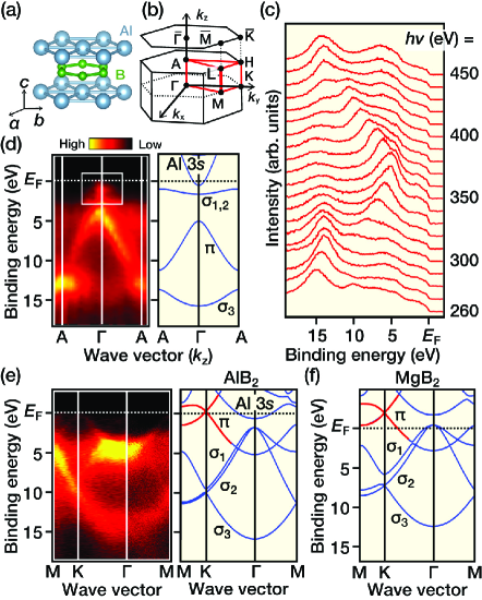
In this regard, AlB2 is one of most suitable materials because the energy bands near the Fermi level () are composed of only and orbitals of light elements (Al and B). As shown in Fig. 1(a), AlB2 is isostructural to well-known high-temperature superconductor MgB2, consisting of alternatively stacking honeycomb B layers and triangular Al lattices. A first-principles band calculation suggests that AlB2 has a linear band crossing (Dirac cone) which arises from the B sub-lattice at the point in the bulk BZ MedvedevaPRB2001 , as in the case of graphene. Due to analogy with multilayer graphene, the band degeneracy at the Dirac point is expected to extend along the direction and form a Dirac nodal line (DNL) along the high-symmetry line LobatoPRB2011 (see Fig. 1b). A similar prediction is also made for isostructural MgB2 JinarXiv2018 . It is therefore urgently required to experimentally establish the DNL in AlB2-type materials and clarify its possible link to the exotic physical properties.
In this Rapid Communication, we report angle-resolved photoemission spectroscopy (ARPES) of AlB2 single crystal. By utilizing bulk-sensitive soft-x-ray photons from synchrotron radiation, we experimentally established the bulk valence band structure in the 3D bulk BZ, and found a highly anisotropic Dirac-cone energy band in the plane which disperses along the direction. This band keeps the degeneracy along the line, producing a characteristic DNL. We discuss implications of the present results by comparing with first-principles band-structure calculations and other topological nodal-line materials.
High-quality single crystals of AlB2 were grown by the Al-flux method. ARPES measurements were performed with a Scienta-Omicron SES2002 electron analyzer with energy-tunable synchrotron light at BL02 in Photon Factory, KEK. We used linearly polarized light (horizontal polarization) of 260-550 eV. The energy and angular resolutions were set to be 150 meV and 0.2∘, respectively. Crystals were cleaved in situ in an ultrahigh vacuum better than 110-10 Torr along the (0001) crystal plane. Sample temperature was kept at = 40 K during ARPES measurements. The Fermi level () of samples was referenced to that of a gold film evaporated onto the sample holder. First-principles band-structure calculations were carried out by QUANTUM ESPRESSO code with generalized gradient approximation QE . The plane-wave cutoff energy and the -point mesh were set to be 30 Ry and 242412, respectively.
We at first performed ARPES measurements along cut perpendicular to the crystal surface [ cut; see Fig. 1(b)] to elucidate the three-dimensionality of electronic structure. Figure 1(c) shows the energy distribution curves (EDCs) at normal-emission setup measured at = 40 K with various photon energies () from 260 to 450 eV. At = 350 eV, a prominent peak is clearly observed at binding energy () of 5 eV, together with a weak hump at around 14 eV. The peak rapidly disperses toward higher on increasing/decreasing from 350 eV, while the hump displays a relatively small dispersion. This distinct dependence of EDCs demonstrates that ARPES measurements with soft-x-ray photons are useful to elucidate the 3D electronic states of AlB2. To better visualize the band dispersions, we plot in Fig. 1(d) the ARPES intensity plotted as a function of and , compared with the calculated band structure. One can immediately identify a highly dispersive band topped at 5 eV at the point and a less dispersive band at 14 eV, which are attributed to the B 2 and bands (here we label three bands as ), respectively, as can be seen from a good agreement in the overall band dispersion between the experiment and calculation. While the calculation predicts weakly dispersive band at 1 eV, the spectral weight of this band appears to be markedly suppressed in ARPES measurements probably due to the matrix-element effect of photoelectron intensity. A closer look at the point with enhanced color contrast (area enclosed by white rectangle) signifies the presence of an electronlike band originating from the Al 3 orbital.
To see the in-plane band dispersions, we plot in Fig. 1(e) the ARPES intensity along the and cuts, measured at = 340 eV (which corresponds to the = 0 plane). A reasonable agreement is seen between the experiment and calculation, e.g., in the highly dispersive band with its bottom of dispersion at 15 eV at , and the linearly dispersive band near around (highlighted by red curve) which forms the Dirac-cone dispersion, as discussed later in detail. The overall spectral feature is consistent with previous ARPES results with vacuum-ultraviolet (VUV) light on AlB2 and MgB2 SoumaAlB2 ; UchiyamaMgB2 ; SoumaMgB2Nature ; TsudaMgB2PRL . Figure 1(f) shows the calculated band structure for MgB2. One immediately recognizes that the band structure is very similar between AlB2 [right panel of Fig. 1(e)] and MgB2 [Fig. 1(f)] except for the location of . The and bands, which are fully occupied in AlB2, are partially occupied in MgB2, and the partially occupied metallic Al 3 band in AlB2 is fully unoccupied in MgB2. This similarity and difference in the electronic band structure between AlB2 and MgB2 is reasonably explained in terms of the same crystal structure with different number of electrons; an Al atom has an extra electron in the outermost shell compared to a Mg atom. The difference in the number of valence electrons provides AlB2 with a great advantage to observe the Dirac-cone dispersion around the point by ARPES, because the Dirac cone situated near in AlB2 is pushed up far above in MgB2, becoming unaccessible by ARPES.
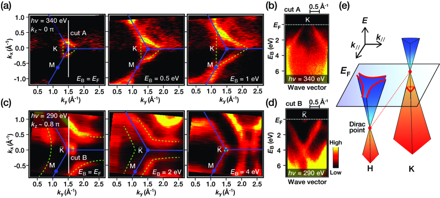
To discuss the spectral feature near in more detail, we show in Fig. 2(a) the ARPES-intensity mapping as a function of in-plane wave vectors ( and ) at representative slices in the plane ( plane) measured with 340-eV photons. At , one can recognize a triangular intensity pattern centered at the point, which is attributed to the band. This triangular pocket originates from the Dirac-cone band with the Dirac point at 0.5 eV above as visible from the band crossing at the point in Fig. 2(b) [note that the crystal is slightly hole doped since the calculated Dirac point is closer to , see Fig. 1(e)]. As seen in Fig. 2(a), the small triangular pocket at the point gradually expands on increasing with keeping its triangular shape, reflecting the band-dispersive feature of lower Dirac cone. This suggests that the Dirac cone is highly anisotropic and reflects the symmetry of the point (). It is noted that a similar triangular-shaped Dirac cone has been observed in doped graphene McChesneyPRB2010 . Such triangular shape of Fermi surface commonly originates from the symmetry of the point and the van Hove singularity of the band dispersion at the point.
We have also mapped out the ARPES intensity as a function of in-plane wave vectors at several slices. Figure 2(c) shows the representative energy contours at obtained with = 290 eV. One immediately recognizes that the intensity distribution is very different from that of = 0 plane [Fig. 2(a)] (note that the ARPES intensity at was found to be very weak and the energy contour cannot be accurately discussed). This is reasonable since AlB2 has a sizable dispersion [see Fig. 1(d)], and the Dirac point is located well below ( 4 eV) in this slice, as visible from the band dispersion in Fig. 2(d). Since the upper Dirac cone touches another Dirac cone located at the adjacent point well above the Dirac point, the energy contour at no longer shows a closed triangular pattern, but exhibits an open arc-like pattern with no -crossing of band on the cut. On increasing , this open contour gradually shrinks toward the point, finally converting into a Dirac point at 4 eV (note that there are several other bands that complicate the intensity pattern). Such behavior is schematically illustrated in Fig. 2(e).
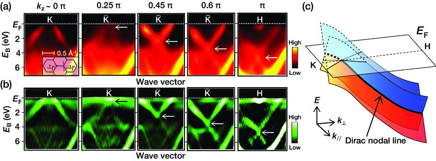
To elucidate how the Dirac-cone band disperses along the direction, we show in Fig. 3(a) the ARPES intensity across the point measured at various ’s, together with the corresponding second-derivative intensity plots [Fig. 3(b)]. In Figs. 3(a) and (b), we observe a linearly dispersive band for all the slices. The Dirac point located at 0.5 eV above at 0 gradually moves downward on increasing , and finally reaches 5 eV below at . Intriguingly, the band always keeps the degeneracy at the point irrespective of with no indication of energy-gap opening. This firmly establishes the presence of a DNL along the whole line in AlB2. The DNL has a finite slope in the - space due to the dispersion of band, as illustrated in Fig. 3(c). It is noted that we surveyed the electronic states over the entire BZ, and found no evidence for the existence of other DNLs in AlB2. This is reasonable since the Dirac cone exists only around the point, as recognized from Fig. 1(e).
Now we discuss characteristics of the observed DNL in AlB2. The observed Dirac-cone band responsible for the DNL originates from the band associated with the honeycomb B layer, which is the same situation as graphene showing the Dirac-cone band with the C-2 character. It was theoretically predicted that when graphene stacks with AA sequence, the Dirac point always keeps the degeneracy irrespective of and forms the DNL along the line LobatoPRB2011 since the sublattice symmetry is preserved in such multilayer graphene. Unfortunately, this situation is not realized in actual graphene since multilayer graphene (graphite) usually stacks with AB or ABC sequence. On the other hand, the honeycomb boron layer in AlB2 stacks with AA sequence, possibly leading to the emergence of DNL in AlB2. However, one may concern that such DNL is easily gapped by the spin-orbit interaction (unless the band degeneracy is protected by nonsymmorphic symmetry), as demonstrated in the gap opening in silicene and germanene C.-C.LiuPRL2011 . But, in the case of AlB2, the SOC is extremely weak (in the level of eV by referring to the atomic SOC value of boron JinarXiv2018 ), so that such problem is overcome, making AlB2 an ideal material to study the behavior of DNL.
It is inferred that the observed DNL in AlB2 has the same origin as that recently predicted for MgB2 JinarXiv2018 , because both materials have essentially the same crystal structure and consequently the same band structure except for the position of the chemical potential (Fermi level) due to the difference in the number of valence electrons (Al has one additional electron compared to Mg). It is therefore suggested that MgB2 also has a DNL and may behave as topological superconductor with nodal fermions contributing to the superconducting pairing. It is noted here that AlB2 is a suitable system to investigate the anomalous transport properties originating from non-zero Berry phase, because it is theoretically proposed that the Landau orbit enclosing the line gives rise to the non-zero Berry phase JinarXiv2018 . This condition is exactly satisfied in AlB2 [see Fig. 2(a)] but not in MgB2. Moreover, by tuning the Al/Mg ratio in (Al,Mg)B2 alloy, we are able to systematically control the electronic phase between the superconducting phase and the non-trivial Berry phase without breaking the DNL. The (Al,Mg)B2 system would provide a precious opportunity to investigate the relationship between topological superconductivity and Berry phase.
Finally, we briefly comment on the relationship between the present results and recent studies on isostructural compounds TiB2 and ZrB2. It has been reported by the first-principles band calculations and ARPES that these compounds have three different types of nodal structures (nodal net) originating from the Ti-3/Zr-4 electrons XFengPRMat2018 ; XZhangPRB2017 ; YiPRB2018 in contrast to the simple DNL in AlB2 originating from the B-2 electrons. While the nodal net of TiB2/ZrB2 is associated with mirror symmetry together with time-reversal and space-inversion symmetry ( symmetry), the DNL of AlB2 is characterized by the sub-lattice symmetry of honeycomb B layer and symmetry. Therefore, the electronic states associated with the nodal fermions and related symmetries are very different between AlB2 and (Ti/Zr)B2, although they share the same crystal structure. The AlB2-type layered diborides would thus serve as an excellent platform to explore a rich variety of nodal fermions and their relationship to symmetries.
In summary, we performed ARPES experiments of AlB2 with bulk-sensitive soft-x-ray photons, and determined the 3D band structure and Fermi surface. We found a triangular-shaped Dirac-cone dispersion at the point of bulk BZ in the - plane. The Dirac cone significantly disperses along the direction while keeping the band degeneracy at the point of surface BZ, producing a characteristic DNL associated with the combination of symmetry and sub-lattice symmetry of honeycomb B layer. The present result paves a pathway toward investigating the exotic nodal structures in weakly spin-orbit-coupled topological materials.
Acknowledgements.
This work was supported by Grant-in-Aid for Scientific Research on Innovative Areas “Topological Materials Science” (JSPS KAKENHI No: JP15H05853), Grant-in-Aid for Scientific Research (JSPS KAKENHI No: JP17H01139, JP18H01160 and JP18H04472), Grant-in-Aid for JSPS Research Fellow (No: JP18J20058) and KEK-PF (Proposal No: 2018S2-001 and 2016G555).References
- (1) Z. Wang, Y. Sun, X.-Q. Chen, C. Franchini, G. Xu, H. Weng, X. Dai, and Z. Fang, Phys. Rev. B 85, 195320 (2012).
- (2) Z. Wang, H. Weng, Q. Wu, X. Dai, and Z. Fang, Phys. Rev. B 88, 125427 (2013).
- (3) M. Neupane, S.-Y. Xu, R. Sankar, N. Alidoust, G. Bian, C. Liu, I. Belopolski, T.-R. Chang, H.-T. Jeng, H. Lin, A. Bansil, F. Chou, and M. Z. Hasan, Nat. Commun. 5, 3786 (2014).
- (4) Z. K. Liu, B. Zhou, Y. Zhang, Z. J. Wang, H. M. Weng, D. Prabhakaran, S.-K. Mo, Z. X. Shen, Z. Fang, X. Dai, Z. Hussain, and Y. L. Chen, Science 343, 864 (2014).
- (5) S. Borisenko, Q. Gibson, D. Evtushinsky, V. Zabolotnyy, B. Buchner, and R. J. Cava, Phys. Rev. Lett. 113, 027603 (2014).
- (6) S. Roth, H. Lee, A. Sterzi, M. Zacchigna, A. Politano, R. Sankar, F. C. Chou, G. Di Santo, L. Petaccia, O. V. Yazyev, and A. Crepaldi, Phys. Rev. B 97, 165439 (2018).
- (7) S.-Y. Xu, I. Belopolski, N. Alidoust, M. Neupane, G. Bian, C. Zhang, R. Sankar, G. Chang, Z. Yuan, C.-C. Lee, S.-M. Huang, H. Zheng, J. Ma, D. S. Sanchez1, B. K. Wang, A. Bansil, F. Chou, P. P. Shibayev, H. Lin, S. Jia, and M. Z. Hasan, Science 349, 613 (2015).
- (8) B. Q. Lv, H. M. Weng, B. B. Fu, X. P. Wang, H. Miao, J. Ma, P. Richard, X. C. Huang, L. X. Zhao, G. F. Chen, Z. Fang, X. Dai, T. Qian, and H. Ding, Phys. Rev. X 5, 031013 (2015).
- (9) L. X. Yang, Z. K. Liu, Y. Sun, H. Peng, H. F. Yang, T. Zhang, B. Zhou, Y. Zhang, Y. F. Guo, M. Rahn, D. Prabhakaran, Z. Hussain, S.-K. Mo, C. Felser, B. Yan, and Y. L. Chen, Nat. Phys. 11, 728 (2015).
- (10) S. Souma, Z. Wang, H. Kotaka, T. Sato, K. Nakayama, Y. Tanaka, H. Kimizuka, T. Takahashi, K. Yamauchi, T. Oguchi, K. Segawa, and Y. Ando, Phys. Rev. B 93, 161112 (2016).
- (11) A. Politano, G. Chiarello, Z. Li, V. Fabio, L. Wang, L. Guo, X. Chen, and D. W. Boukhvalov, Adv. Funct. Mater. 28, 1800511 (2018).
- (12) A. A. Zyuzin and A. A. Burkov, Phys. Rev. B 86, 115133 (2012).
- (13) C.-X. Liu, P. Ye, and X.-L. Qi, Phys. Rev. B 87, 235306 (2013).
- (14) Z. Wang and S.-C. Zhang, Phys. Rev. B 87, 161107 (2013).
- (15) Y. Chen, S. Wu, and A. A. Burkov, Phys. Rev. B 88, 125105 (2013).
- (16) K. Landsteiner, Phys. Rev. B 89, 075124 (2014).
- (17) M. N. Chernodub, A. Cortijo, A. G. Grushin, K. Landsteiner, and M. A. H. Vozmediano, Phys. Rev. B 89, 081407 (2014).
- (18) T. Liang, Q. Gibson, M. N. Ali, M. Liu, R. J. Cava, and N. P. Ong, Nat. Mater. 14, 280 (2015).
- (19) J. Xiong, S. K. Kushwaha, T. Liang, J. W. Krizan, M. Hirschberger, W. Wang, R. J. Cava, and N. P. Ong, Science 350, 413 (2015).
- (20) H. Weng, X. Dai, and Z. Fang, J. Phys.: Condens. Matter 28, 303001 (2016).
- (21) J. W. Rhim and Y. B. Kim, Phys. Rev. B 92, 045126 (2015).
- (22) A. K. Mitchell and L. Fritz, Phys. Rev. B 92, 121109 (2015).
- (23) Y. Huh, E.-G. Moon, and Y. B. Kim, Phys. Rev. B 93, 035138 (2016).
- (24) S. T. Ramamurthy and T. L. Hughes, Phys. Rev. B 95, 075138 (2017).
- (25) A. A. Burkov, M. D. Hook, and L. Balents, Phys. Rev. B 84, 235126 (2011).
- (26) G. Bian, T.-R. Chang, H. Zheng, S. Velury, S.-Y. Xu, T. Neupert, C.-K. Chiu, S.-M. Huang, D. S. Sanchez, I. Belopolski, N. Alidoust, P.-J. Chen, G. Chang, A. Bansil, H.-Tay Jeng, H. Lin, and M. Z. Hasan, Phys. Rev. B 93, 121113(R) (2016).
- (27) H. Weng, Y. Liang, Q. Xu, R. Yu, Z. Fang, X. Dai, and Y. Kawazoe, Phys. Rev. B 92, 045108 (2015).
- (28) W. Chen, H.-Z. Lu, and J.-M. Hou, Phys. Rev. B 96, 041102(R) (2017).
- (29) Z. Yan, R. Bi, H. Shen, L. Lu, S.-C. Zhang, and Z. Wang, Phys. Rev. B 96, 041103(R) (2017).
- (30) X. Feng, C. Yue, Z. Song, Q. Wu, and B. Wen, Phys. Rev. Mater. 2, 014202 (2018).
- (31) X. Zhang, Z.-M. Yu, X.-L. Sheng, H. Y. Yang, and S. A. Yang, Phys. Rev. B 95, 235116 (2017).
- (32) C.-J. Yi, B. Q. Lv, Q. S. Wu, B.-B. Fu, X. Gao, M. Yang, X.-L. Peng, M. Li, Y.-B. Huang, P. Richard, M. Shi, G. Li, O. V. Yazyev, Y.-G. Shi, T. Qian, and H. Ding, Phys. Rev. B 97, 201107(R) (2018).
- (33) G. Bian, T.-R. Chang, R. Sankar, S.-Y. Xu, H. Zheng, T. Neupert, C.-K. Chiu, S.-M. Huang, G. Chang, I. Belopolski, D. S. Sanchez, M. Neupane, N. Alidoust, C. Liu, B. Wang, C.-C. Lee, H.-T. Jeng, C. Zhang, Z. Yuan, S. Jia, A. Bansil, F. Chou, H. Lin, and M. Z. Hasan, Nat. Commun. 7, 10556 (2016)
- (34) D. Takane, K. Nakayama, S. Souma, T. Wada, Y. Okamoto, K. Takenaka, Y. Yamakawa, A. Yamakage, T. Mitsuhashi, K. Horiba, H. Kumigashira, T. Takahashi, and T. Sato, npj Quantum Mater. 3, 1 (2018).
- (35) L. M. Schoop, M. N. Ali, C. Straer, A. Topp, A. Varykhalov, D. Marchenko, V. Duppel, S. S. P. Parkin, B. V. Lotsch, and C. R. Ast, Nat. Commun. 7, 11696 (2016).
- (36) M. Neupane, I. Belopolski, M. M. Hosen, D. S. Sanchez, R. Sankar, M. Szlawska, S.-Y. Xu, K. Dimitri, N. Dhakal, P. Maldonado, P. M. Oppeneer, D. Kaczorowski, F. Chou, M. Z. Hasan, and T. Durakiewicz, Phys. Rev. B 93, 201104(R) (2016).
- (37) D. Takane, Z. Wang, S. Souma, K. Nakayama, C. X. Trang, T. Sato, T. Takahashi, and Y. Ando, Phys. Rev. B 94, 121108(R) (2016).
- (38) N. I. Medvedeva, A. L. Ivanovskii, J. E. Medvedeva, A. J. Freeman, and D. L. Novikov, Phys. Rev. B, 65, 052501 (2001).
- (39) I. Lobato and B. Partoens, Phys. Rev. B 83, 165429 (2011).
- (40) K.-H. Jin, H. Huang, J.-W. Mei, Z. Liu, L.-K. Lim, and F. Liu, arXiv: 1710.06996 (2017).
- (41) P. Giannozzi, S. Baroni, N. Bonini, M. Calandra, R. Car, C. Cavazzoni, D. Ceresoli, G. L. Chiarotti, M. Cococcioni, I. Dabo, A. D. Corso, S. de Gironcoli, S. Fabris, G. Fratesi, R. Gebauer, U. Gerstmann, C. Gougoussis, A. Kokalj, M. Lazzeri, L. Martin-Samos, N. Marzari, F. Mauri, R. Mazzarello, S. Paolini, A. Pasquarello, L. Paulatto, C. Sbraccia, S. Scandolo, G. Sclauzero, A. P. Seitsonen, A. Smogunov, P. Umari, and R. M. Wentzcovitch, J. Phys. Condens. Matter. 21, 395502 (2015).
- (42) S. Souma, T. Sato, T. Takahashi, N. Kimura, and H. Aoki, J. Electron Spectrosc. Relat. Phenom. 144, 545 (2005).
- (43) H. Uchiyama, K. M. Shen, S. Lee, A. Damascelli, D. H. Lu, D. L. Feng, Z.-X. Shen, and S. Tajima, Phys. Rev. Lett. 88, 157002 (2002).
- (44) S. Souma, Y. Machida, T. Sato, T. Takahashi, H. Matsui, S.-C. Wang, H. Ding, A. Kaminski, J. C. Campuzano, S. Sasaki, and K. Kadowaki, Nature 423, 65 (2003).
- (45) S. Tsuda , T. Yokoya, Y. Takano, H. Kito, A. Matsushita, F. Yin, J. Itoh, H. Harima, and S. Shin, Phys. Rev. Lett. 91, 127001 (2003).
- (46) J. L. McChesney, A. Bostwick, T. Ohta, T. Seyller, K. Horn, J. González, and E. Rotenberg, Phys. Rev. Lett. 104, 136803 (2010).
- (47) C.-C. Liu, W. Feng, and Y. Yao, Phys. Rev. Lett. 107, 076802 (2011).