Minimal domain size necessary to simulate the field enhancement factor numerically with specified precision
Abstract
In the literature about field emission, finite elements and finite differences techniques are being increasingly employed to understand the local field enhancement factor (FEF) via numerical simulations. In theoretical analyses, it is usual to consider the emitter as isolated, i.e, a single tip field emitter infinitely far from any physical boundary, except the substrate. However, simulation domains must be finite and the simulation boundaries influences the electrostatic potential distribution. In either finite elements or finite differences techniques, there is a systematic error () in the FEF caused by the finite size of the simulation domain. It is attempting to oversize the domain to avoid any influence from the boundaries, however, the computation might become memory and time consuming, especially in full three dimensional analyses. In this work, we provide the minimum width and height of the simulation domain necessary to evaluate the FEF with at the desired tolerance. The minimum width () and height () are given relative to the height of the emitter (), that is, necessary to simulate isolated emitters on a substrate. We also provide the to simulate arrays and the to simulate an emitter between an anode-cathode planar capacitor. At last, we present the formulae to obtain the minimal domain size to simulate clusters of emitters with precision . Our formulae account for ellipsoidal emitters and hemisphere on cylindrical posts. In the latter case, where an analytical solution is not known at present, our results are expected to produce an unprecedented numerical accuracy in the corresponding local FEF.
pacs:
73.61.At, 74.55.+v, 79.70.+qI Introduction
Carbon nanotubes (CNTs) and carbon nanofibers (CNFs) have attracted great attention in cold field emission applications de Heer et al. (1995); Minoux et al. (2005); Cole et al. (2015, 2014). The ability to design CNT or CNF field emitters with predictable electron emission characteristics allow their use as electron sources in various applications such as microwave amplifiers, electron microscopy, parallel beam electron lithography and advanced X-ray sources Cahay et al. (2014); Cole et al. (2015).
A common practice to model a CNT or CNF is take the emitter as a cylindrical classical conductor capped with a conducting hemisphere, both of radius . The total emitter’s height is . This model is known as the “hemisphere-on-cylindrical post” (HCP), have been extensively studied theoretically Edgcombe and Valdrè (2001); Forbes et al. (2003); Kokkorakis et al. (2002); Read and Bowring (2004); Zeng et al. (2009); Dall’Agnol and den Engelsen (2013); Roveri et al. (2016) and is known to have an analytical counterpart of great complexity as compared with computational solution Forbes et al. (2003). In some studies, the hemi-ellipsoid model is preferred to represent the emitter for a couple of reasons: in this case, the the electrostatic potential distribution in the system has analytical solution and is a better representation of the emitter when the radius at the apex is much smaller than the radius at the base Forbes et al. (2003).
The local field enhancement factor (FEF), particularly at the emitter’s apex (), is an important quantity in field emission science. The apex-FEF facilitates the electron tunneling through the surface barrier and has a dramatic effect on the macroscopic emission current. As a consequence, the FEF makes the emission current very sensitive to the macroscopic electrostatic field, Miller (1967, 1984). For a single-tip field emitter, the relevant characteristic barrier field at the apex may be formally related to by a characteristic apex-FEF Forbes (2012), defined as follows:
| (1) |
Various physical causes of field enhancement can exist, but the more simple assumption is consider the existence of a conducting microprotrusion or nanoprotrusion at the emitter surface Forbes et al. (2003). The question then arises of how the local apex-FEF can be accurately estimated.
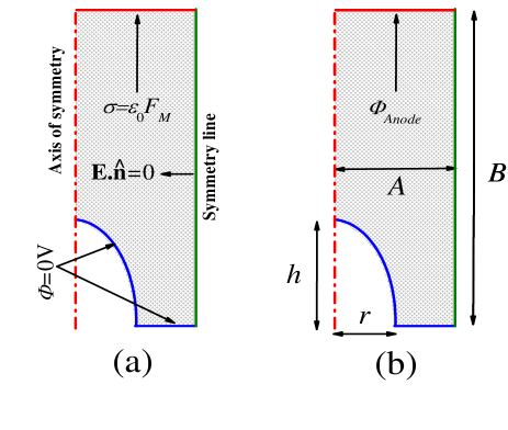
Simulations that involve the solution of Laplace’s equation, whether using finite elements or finite differences, require a minimum volume surrounding the region of interest. The minimum domain size (MDS) depends on the desired precision. If the boundaries are inadvertently close, they will affect the calculated electrostatic potential and the FEF may not respect the desired precision. Then, it might be attempting to overestimate the size of the domain. However, this procedure may become seriously time and memory consuming as the simulated systems become more demanding, mainly in three dimensional (3D) and/or in time-dependent models. Our analysis considers a two dimensional (2D) axisymmetric system, but it is also valid for 3D models, as we will discuss. Hereafter, we adopt the following notation regarding the dimensions of the domain: (i) the variables and are the width and height of the simulation domain as shown in Fig. 1; (ii) the and relative to the height are much better parameters for our analysis. In fact, and are the variables we shall use to determine the systematic error; (iii) the and are the minimum dimensions that induces the tolerated systematic error in the apex-FEF for single tip field emitters.
We start evaluating the minimum width and height of the simulation domain, for single tip field emitter in an semi-infinite space. Then, we discuss why the dimensions found for a single tip field emitter is also valid for emitters in an infinite array and for isolated emitters in a capacitor configuration. Finally, we provide a few numerical values to compare the predictions from our results and the actual simulations. In most cases, the knowledge of is convenient to choose the adequate size of the simulation domain that yields an error of %, which can be considered good in view of the large uncertainties in FE experiments. However, for some analyses, the precision requirement is much larger and must be known. As an example, recently, Forbes has shown that the rate at which the FEF from a pair of spherical emitters tend toward the FEF of a single sphere is given by a power law decay as a function of the separation center to center Forbes (2016). Prior to his work, many authors were assuming an exponential-type decay Gröning et al. (2000); Nilsson et al. (2000); Bonard et al. (2001); Jo et al. (2003); Harris et al. (2015, 2016). This power law was an important realization in the physical mechanism governing the FEF. Since then, the same power law behavior was observed in several different types of emitters like hemispheres on cylindrical posts and ellipsoidal emitters Dall’Agnol et al. (2017); de Assis and Dall’Agnol (2018); Forbes (2018); Biswas and Rudra (2018), provided that the analysis has high precision, as we demonstrated in a previous work de Assis and Dall’Agnol (2018).
This paper is organized as follows. In Section II, the simulation procedures, by using finite element method, are discussed. The results of the MDS, including hemi-ellipsoid single tip field emitter, arrays and capacitor configuration systems, hemisphere on a cylindrical post emitter and full three dimensional models of clusters are discussed on Sec.III. Section IV summarizes our conclusions.
II Simulation procedure
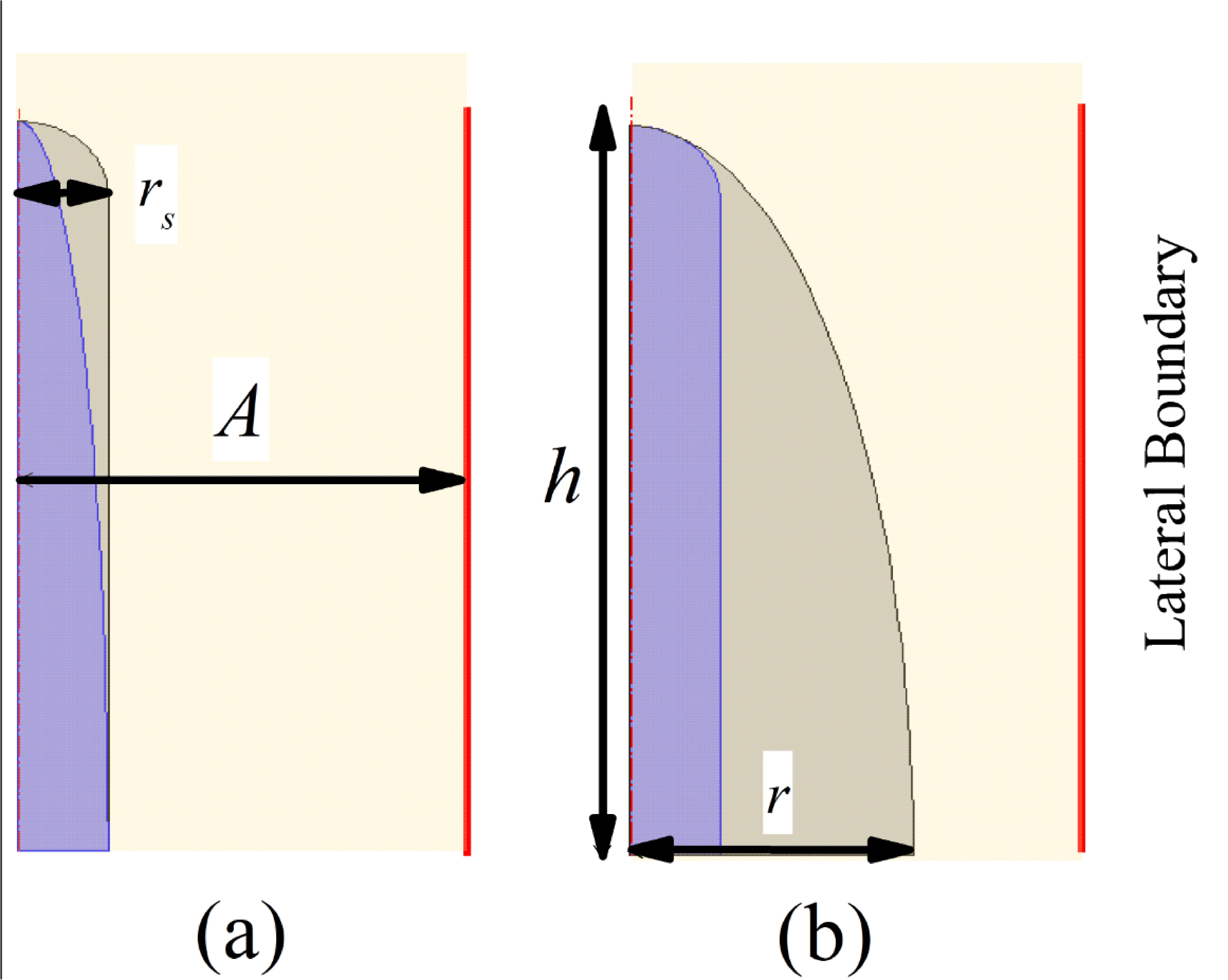
Figure 1 represents the geometries of the physical systems we are interested in minimizing the size. It is a 2D axisymmetric system with a central emitter. We start analyzing an ellipsoidal emitter, for which is known analytically Forbes et al. (2003). Afterward, we shall discuss what errors to expect for emitters like hemispheres on posts and floating spheres. We assume the emitter to be perfectly conductor with no electric field penetration; hence, the interior of the emitter is removed from the simulation domain. The boundary conditions (BCs) on the emitter’s surface and the bottom emitter’s surface are grounded (). The right hand side boundary is a symmetry line, i.e., this BC imposes the electrostatic field to be perpendicular to the normal vector from this boundary line ().
Two distinct BCs are common at the top boundary: Fig. 1(a) represents a single tip field emitter. In this case, the top boundary is set as a surface charge density , where is the permittivity of vacuum. This BC assumes that the anode is much farther than the boundary itself. This is the BC we recommended when assuming that the anode is at infinity, as we shall discuss further. Figure 1(b) represents a single tip field emitter with the top boundary representing the anode with a defined voltage .
We have used the commercial software COMSOL® v.5.3 based on the finite elements method to calculate the apex-FEF. The software evaluates the electrostatic potential distribution and the consequent electrostatic field in the domain. The apex-FEF calculated numerically, is defined as the maximum value of the electrostatic field normalized by the applied field as shown in Eq. (1). Here the index “” indicates a numerical evaluation. We define the error in relative to the analytical values of the field enhancement factor known for hemi-ellipsoidal emitters Forbes et al. (2003):
| (2) |
We want to stress that the analysis in this paper is not limited to any particular method (like finite elements) or computer code. Any computer code will require a MDS to yield a desired precision regardless the numerical precision used in the method. In our analyses, we took care to have enough numerical precision and sufficient number of elements not to compromise the evaluation of , which is solely due to the finite size of the domain. In these analyses, the finite elements were concentrated where the electric field were higher and the number of elements were increased until the solution converged to the necessary precision for our purposes. Although the Boundary Elements Method Read and Bowring (2004) is a better alternative to simulate the FEF, it does not apply in many cases. The MDS we provide here can be useful where the knowledge of the solution in the bulk of the system is necessary. Some examples are: space charge effect, mechanical oscillations in a field emission system or particle tracing analyses.
III Results and Discussion
III.1 Hemi-Ellipsoid single tip field emitter
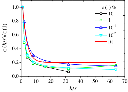
Figure 2(a) illustrates a simple case for a hemispherical emitter, i.e. , where is the radius of the emitter. The converges to its analytical value () as the width and height of the domain increases. Figure 2(b) shows the corresponding systematic error obtained as the height is increased for several normalized widths . In Fig. 2(b) there is the systematic error as a function of the same variables shown in Fig. 2(a). The decays linearly (in log-log scale) until the electrostatic influence from the top boundary becomes smaller than the influence from the lateral boundary and starts to saturate.
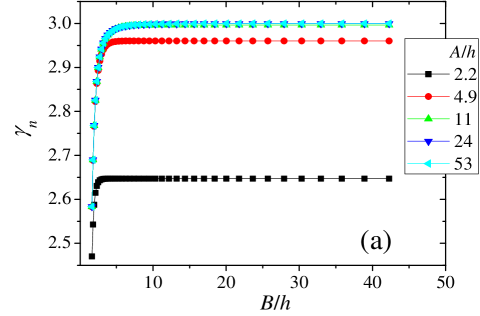
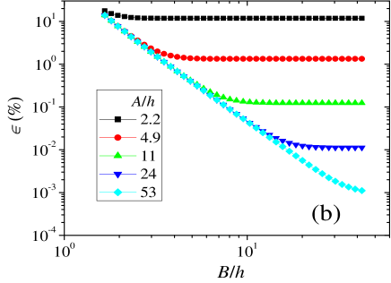
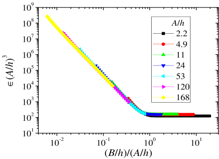
Figure 2(b) can provide the MDS for a few values of . As an example: Fig. 2(b) shows that the curve for has at the saturation, which extends for . Hence, if ones tolerance happens to be , then the leftmost point in the plateau of the curve provide the MDS with and . Better yet, instead of inspecting Fig.2(b) for the MDS, we managed to get a good collapse of all curves by plotting the variables as shown in Fig.3. This is the most important result to obtain the valid for all . In Fig.3, a universal point of minimum can be obtained at the leftmost point in the plateau of the curves. The definition of this point depends on a criterion. In this work we assume to be 10% higher than the value the end of the plateau, which gives and . Then,
| (3) |
and
| (4) |
Equations (3) and (4) are the upper bound of the MDS needed to simulate the apex-FEF with desired error for a unitary aspect ratio. For higher aspect ratios, the MSD is considerably smaller. Figure 4 shows how decreases as increases tending to saturate for . Our analyses show that for any value of or , the can be modeled as
| (5) |
Equation (5) indicates that the error can drop 80% as increases compared with a unitary aspect ratio. The is the error one is interested in having [not ]. Hence, we can replace from Eq. (5) in Eqs. (3) and (4) to incorporate the dependence with in the MDS as follows:
III.2 Arrays and capacitor configuration systems
Our 2D system, as illustrated in Fig. 1, can be used with good approximation to simulate a lattice as described in detail in Ref.Dall’Agnol and den Engelsen (2013). The symmetry boundary acts as a mirror, so the emitter experiences a screening effect due to its own image, similar to the screening in a lattice, where the distance to the neighboring emitters is . Equations (6) and (7) apply straightforwardly to simulate arrays or an isolated emitter in a capacitor configuration. However, it is necessary to interpret as the actual tolerated systematic error, not the error defined in Eq. (2). For example, if one is interested in simulating a compact array with , then the electrostatic influence form the lateral boundary (which is fixed to ) causes , as defined in Eq. (2), to be larger than 1%. However, the electrostatic influence from the symmetry boundary is not an error in the calculations; it is necessary to compute the fractional reduction in the FEF in arrays. The only electrostatic influence that has to be avoided is the influence from the top boundary, which is already granted to be less than 1% if from Eq.(7) is respected. The same is valid for a capacitor configuration. In this case, the influence from the top boundary is necessary to compute the FEF correctly. However, for as long as from Eq. (6) is calculated with the desired tolerance , then the error from the lateral boundary will be smaller than .
III.3 Hemisphere on a cylindrical post emitter - HCP model
The HCP geometry is a classical representation of CNT emitters, so it is an important case to be analyzed here. For unitary aspect ratio, hemi-ellipsoids becomes hemispheres, so Eqs. (3) and (4) gives the MDS either for ellipsoid or HCP as an upper limit for the MDS. However, the improved MDS as a function of the aspect ratio does not scale for the HCP as it does for ellipsoids [Eqs. (6) and (7)]. Note, in Fig. 5(a) an HCP is superposed to an ellipsoid with same aspect ratio. The surface of the HCP is closer to the lateral boundary, so the boundary’s influence is greater over the HCP then it is over the ellipsoid, implying that Eqs. (6) and (7) does not grant to be smaller than . Nevertheless, we can compare an HCP and an ellipsoid with same radius of curvature at the apex, as shown in Fig. 5(b). In this case, the for the HCP is granted to be smaller than . Hence, we can safely use Eqs. (6) and (7) to evaluate the MDS for HCPs if we use the aspect ratio of the circumscribed ellipsoid, instead of the actual aspect ratio of the HCP. To do so, we must find the relation between the aspect ratio of the circumscribed ellipsoid as a function of the aspect ratio of the HCP.
Let be the curvature of the hemispherical cap that equals the curvature of the ellipsoid at the apex (). The curvature () is simply the absolute value of the second derivative of the ellipsoid function . Therefore:
| (8) |
which results in the following relation for the aspect ratios:
| (9) |
Finally, we can improve the MDS for HCP as a function of the aspect ratio by replacing in Eqs. (6) and (7) for . As a last note, the procedure we did in section III.1 cannot be used to determine the MDS for HCPs, because, at present, there is not an analytical solution for the electrostatic potential distribution for single tip HCP emitters. However, the results presented here for this model are expected to significatively advances to obtain numerical values of with unprecedented accuracy.
III.4 Full 3D models of clusters
To determine the MDS for cluster is somewhat more complicated. Clusters of emitters do not present rotational symmetry and cannot be simulated in a 2D axisymmetric model. Even then, Eqs. (6) and (7) still grants an error slightly smaller than the tolerance, because the boundaries in a full 3D model cause less electrostatic influence over the emitters, as explained in Ref.Dall’Agnol and den Engelsen (2013). However, the distance from the center of the system to the lateral boundary is not a parameter of merit in clusters. Instead, we are interested in the minimal distance from the outmost emitter to the lateral boundary. To avoid confusion, let be the distance from the outer emitter to the boundary.
For clusters, the at a particular emitter must be equal (in the condition for the MDS) to the summation of the errors caused by all emitters:
| (10) |
where is number of emitter in the cluster. To evaluate , we must be careful to consider the maximum influence that the boundary causes on the outmost emitter in the cluster. Consider only two emitter as shown in Fig. 6. The image of emitter (indicated as ) with respect to the lateral boundary generates an error in its own FEF, which is simply the inverse function of Eq. (6), given by:
| (11) |
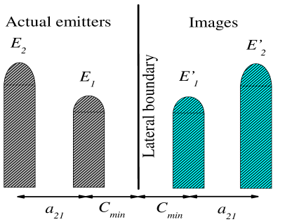
Parameters and does not need to be the same for all emitters. Therefore, these parameters gain a sub-index (), corresponding to the -th emitter. The image of (indicated as ) generates an error on according to the distance from to the lateral boundary plus the distance () from to . Now it is important to note that Eqs. (6), (7) and (11) assume implicitly that the image of the emitter is at a distance twice farther than the boundary. Therefore, to compute the error due to the influence of on , we must use half the distance between these (which is ), independently of the boundary’s position. Hence, we have:
| (12) |
where is known. The influence of construction in Eq. (12) makes always larger than the error expected for isolated, which grants the total error to be lower than the tolerance. Replacing Eqs. (11) and (12) in (10), we get:
| (13) |
where . The in Eq. (13) cannot be isolated, but can be solved straightforwardly using numerical methods (like Newton’s method, for example). Finally, in a cluster with emitters, we just have to replace the upper limit of the summation in Eq. (13) to . Similarly, we can obtain the minimum distance to the top boundary as:
| (14) |
where is the distance from the top of the tallest emitter to the top boundary, is the height of the tallest emitter and is the difference between the tallest emitter and the -th emitter. In Eq. (14) we do not consider the relative positions amongst the emitter in the cluster, only the heights relative to the top boundary.
Remember, if the emitter in the clusters are HCPs, the aspect ration , must be replaced by as discussed.
III.5 Table for reference and verification of the MSD method
IV Conclusions
We provided the MDS of the simulation domain and necessary to simulate the apex-FEF with a systematic error smaller than a given . We summarize the results as follows:
(i) For a hemi-ellipsoid single tip field emitter (STFE), with a given aspect ratio (), the MDS is
| (15) |
and
| (16) |
(ii) For a planar hemi-ellipsoid capacitor system, is fixed and
| (17) |
(iii) For an infinite array formed by hemi-ellipsoid emitters, is fixed and
| (18) |
(iv) For HCP emitters, the MDS is the same as in Eqs. (15), (16), (17) and (18), except that the aspect ratio must be replaced to .
To simulate isolated emitters, arrays or clusters of emitters, our results are only valid when using Neumann BC at top and right hand side boundaries, which the authors strongly recommend. The Neumann BC generates systematic errors much smaller than the Dirichlet BC for a given domain size; typically by a factor of . In other words, the MDS using a specified voltage at the contours of the simulation domain should be bigger to yield the same precision. We expect our results be a major assistance for the field emission community to obtain accurate FEF in systems where the analytical electrostatic solution is still unknown.
V Acknowledgements
TAdA acknowledges Royal Society under Newton Mobility Grant, Ref: NI160031. The authors are thankful to the Brazilian Council of Science and Technology (CNPq) and to Richard Forbes for his suggestions and discussions.
References
- de Heer et al. (1995) W. A. de Heer, A. Châtelain, and D. Ugarte, Science 270, 1179 (1995).
- Minoux et al. (2005) E. Minoux, O. Groening, K. B. K. Teo, S. H. Dalal, L. Gangloff, J.-P. Schnell, L. Hudanski, I. Y. Y. Bu, P. Vincent, P. Legagneux, G. A. J. Amaratunga, and W. I. Milne, Nano Letters 5, 2135 (2005).
- Cole et al. (2015) M. T. Cole, M. Mann, K. B. Teo, and W. I. Milne, in Emerging Nanotechnologies for Manufacturing (Second Edition), Micro and Nano Technologies, edited by W. Ahmed, , and M. J. Jackson (William Andrew Publishing, Boston, 2015) second edition ed., pp. 125 – 186.
- Cole et al. (2014) M. Cole, K. B. K. Teo, O. Groening, L. Gangloff, P. Legagneux, and W. I. Milne, Sci. Rep. 4, 4840 (2014).
- Cahay et al. (2014) M. Cahay, P. T. Murray, T. C. Back, S. Fairchild, J. Boeckl, J. Bulmer, K. K. K. Koziol, G. Gruen, M. Sparkes, F. Orozco, and W. O’Neill, Applied Physics Letters 105, 173107 (2014).
- Edgcombe and Valdrè (2001) C. J. Edgcombe and U. Valdrè, Journal of Microscopy 203, 188 (2001).
- Forbes et al. (2003) R. G. Forbes, C. Edgcombe, and U. Valdrè, Ultramicroscopy 95, 57 (2003).
- Kokkorakis et al. (2002) G. C. Kokkorakis, A. Modinos, and J. P. Xanthakis, Journal of Applied Physics 91, 4580 (2002).
- Read and Bowring (2004) F. Read and N. Bowring, Nuclear Instruments and Methods in Physics Research Section A: Accelerators, Spectrometers, Detectors and Associated Equipment 519, 305 (2004), proceedings of the Sixth International Conference on Charged Particle Optics.
- Zeng et al. (2009) W. Zeng, G. Fang, N. Liu, L. Yuan, X. Yang, S. Guo, D. Wang, Z. Liu, and X. Zhao, Diamond and Related Materials 18, 1381 (2009).
- Dall’Agnol and den Engelsen (2013) F. F. Dall’Agnol and D. den Engelsen, Nanoscience and Nanotechnology Letters 5, 329 (2013).
- Roveri et al. (2016) D. Roveri, G. Sant’Anna, H. Bertan, J. Mologni, M. Alves, and E. Braga, Ultramicroscopy 160, 247 (2016).
- Miller (1967) H. C. Miller, Journal of Applied Physics 38, 4501 (1967).
- Miller (1984) H. C. Miller, Journal of Applied Physics 55, 158 (1984).
- Forbes (2012) R. G. Forbes, Nanotechnology 23, 095706 (2012).
- Forbes (2016) R. G. Forbes, Journal of Applied Physics 120, 054302 (2016).
- Gröning et al. (2000) O. Gröning, O. M. Küttel, C. Emmenegger, P. Gröning, and L. Schlapbach, Journal of Vacuum Science & Technology B: Microelectronics and Nanometer Structures Processing, Measurement, and Phenomena 18, 665 (2000).
- Nilsson et al. (2000) L. Nilsson, O. Groening, C. Emmenegger, O. Kuettel, E. Schaller, L. Schlapbach, H. Kind, J.-M. Bonard, and K. Kern, Applied Physics Letters 76, 2071 (2000).
- Bonard et al. (2001) J.-M. Bonard, N. Weiss, H. Kind, T. Stöckli, L. Forró, K. Kern, and A. Châtelain, Advanced Materials 13, 184 (2001).
- Jo et al. (2003) S. H. Jo, Y. Tu, Z. P. Huang, D. L. Carnahan, D. Z. Wang, and Z. F. Ren, Applied Physics Letters 82, 3520 (2003).
- Harris et al. (2015) J. R. Harris, K. L. Jensen, and D. A. Shiffler, AIP Advances 5, 087182 (2015).
- Harris et al. (2016) J. R. Harris, K. L. Jensen, W. Tang, and D. A. Shiffler, Journal of Vacuum Science & Technology B 34, 041215 (2016).
- Dall’Agnol et al. (2017) F. F. Dall’Agnol, T. A. de Assis, and R. G. Forbes, in 30th International Vacuum Nanoelectronics Conference (IVNC) (2017) pp. 230–231.
- de Assis and Dall’Agnol (2018) T. A. de Assis and F. F. Dall’Agnol, Journal of Physics: Condensed Matter 30, 195301 (2018).
- Forbes (2018) R. G. Forbes, arXiv:1803.03167 (2018).
- Biswas and Rudra (2018) D. Biswas and R. Rudra, arXiv:1805.07286v1 (2018).