Large spin current generation by the spin Hall effect in mixed crystalline phase Ta thin films
Abstract
Manipulation of the magnetization in heavy-metal/ferromagnetic bilayers via the spin-orbit torque requires high spin Hall conductivity of the heavy metal. We measure inverse spin Hall voltage using a co-planar wave-guide based broadband ferromagnetic resonance set-up in Py/Ta system with varying crystalline phase of Ta. We demonstrate a strong correlation between the measured spin mixing conductance and spin Hall conductivity with the crystalline phase of Ta thin films. We found a large spin Hall conductivity of cm-1 for low-resistivity (68 –cm) Ta film having mixed crystalline phase, which we attribute to an extrinsic mechanism of the spin Hall effect.
- Keywords
-
Spin Hall effect, Ta thin films, Spin mixing conductance, Inverse spin Hall effect
pacs:
Valid PACS appear hereSpin Hall effect (SHE) can be used to produce a pure transverse spin current density () from a longitudinal electrical current density () in heavy metals. Dyakonov and Perel (1971); Hirsch (1999) The pure spin current can be measured using the reciprocal effect, i.e., the inverse spin Hall effect (ISHE) employing a transverse charge current created from the pure spin current. The spin current can generate a current-induced spin-orbit torque (SOT) in heavy metal/ferromagnet (HM/FM) heterostructure for potential application in the efficient manipulation of magnetization at the nanoscale. Liu et al. (2011, 2012a) With sufficiently strong SOT, it is possible to excite magnetization to auto-oscillation for radio frequency generation application Liu et al. (2012b); Demidov et al. (2012); Tiwari et al. (2017) or switch the magnetization, move domain walls or skyrmions for efficient memory applications. Liu et al. (2012a); Miron (2014); Liu et al. (2012b); Bhowmik et al. (2014)
For realizing these applications, a large spin Hall angle, defined as the ratio of the spin current density to the charge current density is desirable. While the value of in most commonly investigated metal Pt is , Ando et al. (2008); Liu et al. (2011); Azevedo et al. (2011); Sinova et al. (2015) recent results show relatively higher spin Hall angle of in Ta,Morota et al. (2011); Liu et al. (2012a); Hao and Xiao (2015); Allen et al. (2015); Kim et al. (2015); Niimi and Otani (2015); Qiu et al. (2014); Deorani and Yang (2013); Hahn et al. (2013); Vélez et al. (2016); Emori et al. (2013) and of the order of for W. Pai et al. (2012); Demasius et al. (2016); Hao and Xiao (2015) However, these higher values of in Ta and W are so far reported in very high resistive phase of these materials, which limits several applications that require a charge current to flow in the HM.
In this work, we report a strong correlation of spin Hall angle with the crystalline phase of Ta thin films in Py/Ta bilayers. The crystalline phase of Ta films is varied by controlling growth rate in sputtering. We develop and demonstrate a simple method for measurement of ISHE using a broadband ferromagnetic resonance (FMR) set-up without involving micro-fabrication. We show that the voltage measured in our optimized set-up primarily arises from ISHE by using out-of-plane angle dependence and radio frequency (RF) power dependence, which rules out voltage signal due to other galvanomagnetic effects such as anisotropic magneto-resistance (AMR) and anomalous Hall effect (AHE). We find a higher spin mixing conductance and spin Hall conductivity (cm-1) for low resistivity Ta having mixed crystalline phase, which is promising for applications. The large spin Hall conductivity for mixed crystalline phase Ta is consistent with the extrinsic mechanism of spin Hall effect.
The Py( nm)/Ta(20 nm) bilayer thin films are prepared on Si substrates using DC-magnetron sputtering at a working and base pressure of and Torr, respectively. We first studied single layer Ta thin films with different growth rates by varying the DC-sputtering power. Subsequently, Py( nm)/Ta(20 nm) bilayer thin films were prepared with varying thickness of Py, and growth rate of Ta. The Ta thickness was kept fixed at 20 nm. Before the deposition of the different layers, pre-sputtering of the targets was performed for 10 min with a shutter. Crystallographic properties of films were determined using X-ray diffraction (XRD) while the thicknesses and interface/surface roughness were determined from X-ray reflectivity (XRR) technique using a PANalytical X’Pert diffractometer with Cu-Kα radiation. The XRR data (not shown) was fitted using the recursive theory of Parratt. Parratt (1954) From XRR fitting the surface and interface roughness were found to be 0.5 nm.
Ferromagnetic resonance (FMR) measurements are carried out for excitation frequencies of 4–12 GHz at room temperature. We use a co-planar waveguide (CPW) based broad-band FMR set-up. Bansal et al. (2018) For a fixed excitation frequency of microwave field, external magnetic field () is swept for the resonance condition. The ISHE measurements are performed on mm2 samples by measuring voltage signal at the edge of the samples by fabricating 100 m-thick Cu contact pads. This geometry allows us to measure ISHE signal in our samples when the film side is facing the CPW.
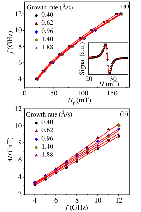
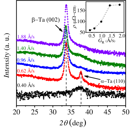
Figure 1 shows the XRD spectra for single layer 50 nm-thick Ta thin films prepared at different growth rates by varying sputtering power in DC magnetron sputtering. A broad diffusive peak of -phase of Ta centered around 2 is observed for thin films grown at the lowest growth rate of 0.40 Å/s. This peak corresponds to (110) reflection of Ta. Bragg peaks corresponding to (002) -Ta and (110) -Ta are observed for growth rates between 0.62 Å/s and 1.4 Å/s, respectively, which suggest the growth of a mixed (+) phase of Ta. However, an oriented -phase of Ta is observed for growth rate higher than 1.4 Å/s with Bragg reflections at 2 = 33.6∘ corresponding to -Ta (002) reflection. Inset of Fig. 1 shows the resistivity measurements on 20 nm Ta thin films grown with varying growth rate, measured using Van der Pauw method. The samples with pure -phase of Ta shows a higher resistivity of about 180 –cm which is in agreement with literature. Liu et al. (2012a) For the -phase the resistivity is found to be around 60 –cm.
The measured FMR data are shown in Fig. 2 for Py(30 nm)/Ta(20 nm) bilayer structure, where Ta is grown at a growth rate of 0.62 /s at which a mixed (+) phase of Ta is formed. The raw FMR spectra are fitted with the sum of derivative of symmetric and asymmetric Lorentzian functions: Woltersdorf (2004)
| (1) |
where , , and are the measured field, FMR linewidth (half width at half maximum; HWHM) and resonance field, respectively. and are the symmetric and asymmetric amplitudes of the voltage signal, respectively. An example of FMR spectra with the fitting is shown in the inset of Fig. 2(a).
From the fittings of FMR spectra, the linewidth and the resonance field () are determined. The as a function of frequency () is shown in Fig. 2(a), which was fitted with Kittel equation: Kittel (1948)
| (2) |
where, is the effective saturation magnetization and is the anisotropy field. Here, =1.85 GHz/T is the gyromagnetic ratio.
The Gilbert damping parameter, was calculated from the slope of the vs. [Fig. 2(b)] by fitting with following equation:
| (3) |
where is inhomogeneous line broadening, which is related with the film quality. In our experimental results [Fig. 2(b)], the vs. shows a linear behavior indicating the intrinsic origin of damping parameter observed in our Py/Ta bilayers thin films. We have also observed very small value of ( mT), which further confirms the high-quality of these thin films. For quantifying spin pumping for different Ta crystalline phase, we have performed Py thickness dependence of and for varying crystalline phase of Ta. Figure 3(a) shows damping parameter vs. inverse of Py thickness for the different crystalline phase of Ta thin films. We then calculate the spin mixing conductance, which is an important parameter that determines the spin pumping efficiency. According to the theory of spin pumping, Tserkovnyak et al. (2002)
| (4) |
where, and are Landé -factor and Bohr magneton, respectively. We have calculated by fitting Gilbert damping parameter versus inverse of Py thickness with above equation as shown in Fig. 3(a). We used for Ni80Fe20 for calculating Shaw et al. (2013) In Eq (4), we neglected the spin back flow, since the Ta thickness we used is quite large compared to reported spin diffusion length of Ta. Liu et al. (2012a); Emori et al. (2013); Wang et al. (2014); Kim et al. (2015); Allen et al. (2015); Behera et al. (2016)
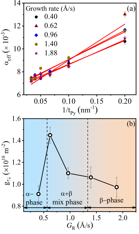
Figure 3(b) shows the value of with varying growth rate of Ta thin films. Interestingly, the highest value of is observed for the mixed phase of Ta. In a recent study, we showed that the spin current efficiency is maximum for the mixed phase Ta using an optical technique. Bansal et al. (2017) Thus, the higher value of for mixed phase Ta is consistent with this earlier study. The spin mixing conductance, determines the amount of spin current injected to the non-magnetic Ta layer. A variation of with crystalline phase, imply a change of effective spin current injected to the Ta layer. Hence, a correlation between and the inverse spin Hall voltage is expected. For this, we measured ISHE in these bilayers as a function of the crystalline phase of Ta thin films. The upper panel in Fig. 4(a) shows an example of ISHE voltage signal observed for the Py/Ta thin film for the growth rate of 0.62 /s.
In our measurement, we have used a field-modulation method to enhance the sensitivity. Tiwari et al. (2016) In this method, the static field is modulated with a small ac field (98 Hz) of magnitude 0.5 mT, produced by a pair of Helmholtz coils. These coils are powered by the lock-in amplifier, which also measures the voltage across the sample. Thus, the field modulation method measures essentially the derivative signal. However, the most reported literature on ISHE uses amplitude modulation of RF signal. Mosendz et al. (2010a, b); Ando et al. (2011); Deorani and Yang (2013); Gupta et al. (2017) Hence, in the lower panel of Fig. 4(a), we show the integrated ISHE signal for better comparison with the literature. The measured signal in our system may consist of ISHE in the Ta layer, and the AMR or AHE of the Py layer. The AMR or AHE is often assumed to produce an asymmetric Lorentzian shape while the ISHE is assumed to produce a symmetric Lorentzian shape Mosendz et al. (2010b); Ando et al. (2011); Ando and Saitoh (2012); Bai et al. (2013); Iguchi and Saitoh (2017) so that the measured data is a sum of symmetric and asymmetric Lorentzian functions. Our measured ISHE spectra are symmetric in shape and changes sign with inversion of magnetic field direction which indicates that the voltage signal we measure may be primarily due to ISHE. Mosendz et al. (2010a, b); Ando et al. (2011); Deorani and Yang (2013)
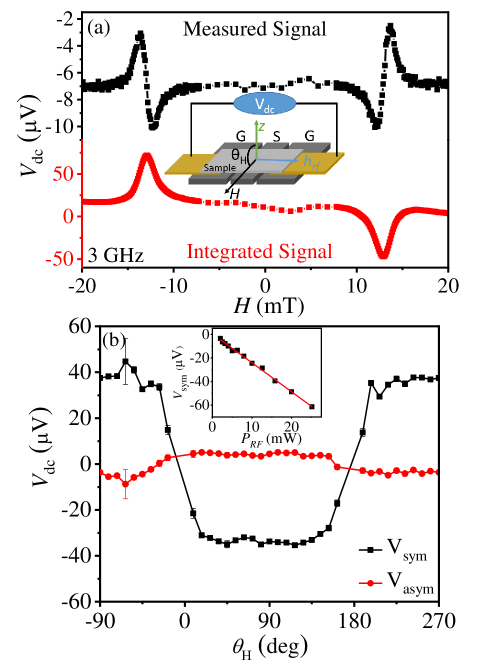
To further verify that the measured signal is indeed from the ISHE, we measured the voltage in our samples by changing the direction of magnetic field out-of-the film plane. The measurement geometry is shown in the inset of Fig. 4(a). Here, the out-of-plane angle () is measured from the z-axis, so that corresponds to the out-of-plane direction. Figure 4(b) shows the variation of symmetric and asymmetric voltage components with varying . According to Lustikova et. al., the asymmetric component () can arise due to the AMR and AHE while the symmetric component () arises due to ISHE, as well as AMR and AHE. Lustikova et al. (2015) In our measurements, we found for the entire range of . Also, the observed angular dependence of is not analogous to the analysis presented by Lustikova et al.. Lustikova et al. (2015) This indicates that the voltage signal measured in our set-up is primarily due to the ISHE. Furthermore, the increases linearly with radio frequency(RF) power as shown in the inset of Fig. 4(b), which is also consistent with ISHE. Ando et al. (2011)
Based on the above observations, we took the symmetric signal as ISHE () for calculating the spin Hall angle () of Ta. The spin Hall angle relates to the ISHE voltage in the following manner: Ando and Saitoh (2010); Mosendz et al. (2010a); Deorani and Yang (2013); Wang et al. (2014); Gupta et al. (2017)
| (5) |
where, is the ISHE signal induced by spin pumping, is the sample resistance measured from Py/Ta samples, is the length of the sample, and are thickness and spin diffusion length of Ta thin film, respectively. The spin diffusion length of Ta thin films is taken to be 2.47 nm measured in similar bilayer structures. Behera et al. (2016) As a first approximation, we neglect the possible variation of with the crystalline phase of Ta. This assumption is very much valid in our case as the thickness of Ta is very large compared to the reported values of the spin diffusion length of Ta, which is of the order of 0.4–3 nm Liu et al. (2012a); Emori et al. (2013); Wang et al. (2014); Kim et al. (2015); Liu et al. (2015); Allen et al. (2015); Behera et al. (2016, 2017) so that in the above equation. The spin back flow is also negligible for the same reason i.e., . is the correction factor and comes from the fact that only a part of the sample contributes to the spin pumping and it depends upon the area of the sample above the signal line of CPW. The value of can be calculated using the method discussed by P. Deorani et al. Deorani and Yang (2013) by noting that the width () of signal line is 185 wide and distance between contact pads is 2 mm and spin wave propagation length of Ta is about 25 . Kwon et al. (2013)
is spin current density and can be defined as,
| (6) |
where, is the angular frequency of microwave excitation, is real part spin mixing conductance. is the magnetization precession cone angle given by , where is the strength of RF field experienced by the sample. This field is generated around the signal line as a result of RF current flow. The value of is obtained from Ampere’s law, , where and is the width of signal line and separation between signal line to sample (0.5 mm), is the applied RF power and is the impedance of CPW i.e., 50 . is the ellipticity correction factor and arises from the ellipticity of the magnetization precession. As the magnetization precession in a magnetic thin film is not exactly circular, but follows an elliptical path due to strong demagnetizing fields. According to Ando et al.Ando1a et al. (2009), is given by,
| (7) |
where, . As explained by Mosendz et al.Mosendz et al. (2010a), the value of ellipticity correction factor changes by a multiple of more than 3 for frequency range 2 to 8 GHz and becomes larger than 1 for frequencies higher than 10 GHz. This shows that magnetization precession trajectory is very elliptical for lower frequencies and DC voltage due to ISHE requires this correction factor.
After considering all the required terms, the value of the spin Hall angle of the Ta thin films can be calculated using Eq. (5).
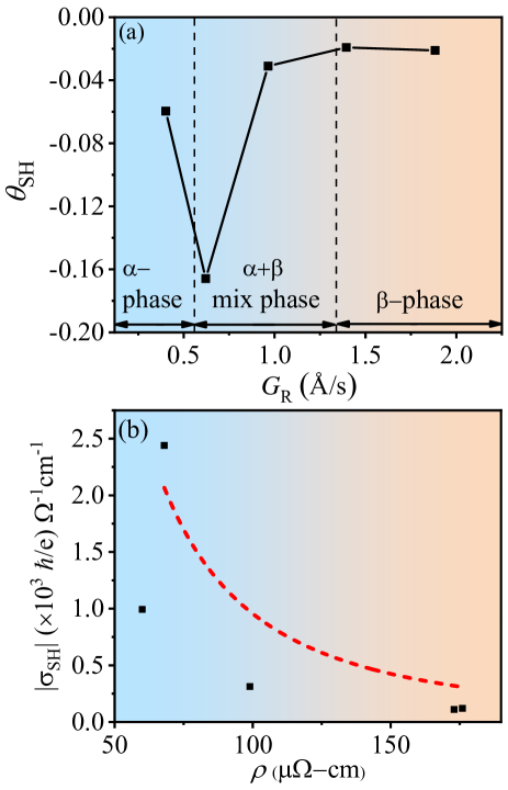
We found the sign of spin Hall angle to be negative, which was confirmed by measuring a Py/Pt sample (not shown) for which the sign was found positive which is consistent with the literature. Figure 5 shows the variation of spin Hall angle with varying growth rate of Ta, measured at 3 GHz. The results show a strong correlation between the spin Hall angle and crystalline phase of Ta. Furthermore, the behavior of spin Hall angle is similar to the variation of spin mixing conductance shown in Fig. 3(b) indicating a strong correlation between the spin-mixing conductance and the inverse spin Hall effect. This correlation further confirms that spin rectification effects are negligible in our measurement, unlike a recent study where spin-mixing conductance and the inverse spin Hall effect were found to be uncorrelated due to the presence of spin rectification effects. Conca et al. (2017)
Surprisingly, it is observed that the low-resistivity Ta thin films with mixed phase show the highest value of spin Hall angle, . The highest value of spin Hall angle reported in the literature for Ta is , which was for the high resistive -phase of Ta. Emori et al. (2013) In our case, we observed a lower spin Hall angle of for the high resistive -phase of Ta. We calculate the spin Hall conductivity, using the following formula:
| (8) |
where, is the charge conductivity of the Ta thin films. We found the spin Hall conductivity, to be around -2439 cm-1 for low-resistivity Ta having mixed crystalline phase for the sample grown at a growth rate of 0.62 /s. To our knowledge, no theoretical calculation exists for the polycrystalline mixed phase Ta films. However, first principle calculation show that the intrinsic spin Hall conductivity of Ta is cm-1, while that of Ta is cm-1. Qu et al. (2018) Hence, the significantly higher value of , that we obtain for the mixed phase Ta is likely caused by extrinsic mechanism. The intrinsic and extrinsic contributions to the spin Hall conductivity can be written in the following manner:Tian et al. (2009); Isasa et al. (2015); Ramaswamy et al. (2017); Sagasta et al. (2018)
| (9) |
where, is intrinsic spin Hall conductivity, is the spin Hall conductivity due to side jump mechanism, is the skew scattering angle and is the longitudinal resistivity of Ta at room temperature, and is the residual resistivity of Ta. In Fig. 5(b), we plot the measured versus . The figure shows a strong dependence of with indicating that the in these films is influenced by both the intrinsic and extrinsic contributions. In particular, for the mixed phase Ta films, increases when decreases as predicted by Eq. (9). Assuming that is independent of crystalline phase, we expect , which is shown by the dashed line. The experimental behavior nearly follows this dependence except for the phase Ta. Thus, from Fig. 5 (b) one can conclude that the large spin Hall conductivity in the mixed phase Ta films is due to the extrinsic mechanism of spin Hall effect. Though a more detailed microscopic examination of samples is needed to find the exact origin of defects in the mixed phase Ta, the results do support the extrinsic mechanism of spin Hall effect in the Ta thin films.
In summary, we have measured inverse spin Hall voltage (ISHE) in Py/Ta system by varying the crystalline phase of Ta using a co-planar wave-guide based broadband ferromagnetic resonance set-up. We demonstrate a strong correlation of measured spin mixing conductance and spin Hall conductivity with the crystalline phase of Ta thin films. We found a large spin Hall conductivity of cm-1 for low-resistivity (68 –cm) Ta having mixed crystalline phase, due to the extrinsic mechanism of spin Hall effect. The study is useful for the efficient manipulation of magnetization at the nanoscale as well as for explaining the spread in the values of spin Hall angle of Ta in literature.
The partial support from the Ministry of Human Resource Development under the IMPRINT program, the Department of Electronics and Information Technology (DeitY), and Department of Science and Technology under the Nanomission program are gratefully acknowledged. A. K. acknowledges support from Council of Scientific and Industrial Research (CSIR), India.
References
- Dyakonov and Perel (1971) M. I. Dyakonov and V. I. Perel, Phys. Lett. A 35, 459 (1971).
- Hirsch (1999) J. E. Hirsch, Phys. Rev. Lett. 83, 1834 (1999).
- Liu et al. (2011) L. Liu, T. Moriyama, D. C. Ralph, and R. A. Buhrman, Phys. Rev. Lett. 106, 036601 (2011).
- Liu et al. (2012a) L. Liu, C.-F. Pai, Y. Li, H. W. Tseng, D. C. Ralph, and R. A. Buhrman, Science 336, 6081 (2012a).
- Liu et al. (2012b) L. Liu, C.-F. Pai, D. C. Ralph, and R. A. Buhrman, Phys. Rev. Lett. 109, 186602 (2012b).
- Demidov et al. (2012) V. E. Demidov, S. Urazhdin, H. Ulrichs, V. Tiberkevich, A. Slavin, D. Baither, G. Schmitz, and S. O. Demokritov, Nat. Mater. 11, 1028 (2012).
- Tiwari et al. (2017) D. Tiwari, N. Behera, A. Kumar, P. Dürrenfeld, S. Chaudhary, D. K. Pandya, J. Åkerman, and P. K. Muduli, Appl. Phys. Lett. 111, 232407 (2017).
- Miron (2014) I. M. Miron, Nat. Nano. 9, 502 (2014).
- Bhowmik et al. (2014) D. Bhowmik, L. You, and S. Salahuddin, Nat. Nano. 9, 59 (2014).
- Ando et al. (2008) K. Ando, S. Takahashi, K. Harii, K. Sasage, J. Ieda, S. Maekawa, and E. Saitoh, Phys. Rev. Lett. 101, 036601 (2008).
- Azevedo et al. (2011) A. Azevedo, L. H. Vilela-Leão, R. L. Rodríguez-Suárez, A. F. LacerdaSantos, and S. M. Rezende, Phys. Rev. B 83, 144402 (2011).
- Sinova et al. (2015) J. Sinova, S. O. Valenzuela, J. Wunderlich, C. H. Back, and T. Jungwirth, Rev. Mod. Phys. 87, 1213 (2015).
- Morota et al. (2011) M. Morota, Y. Niimi, K. Ohnishi, D. H. Wei, T. Tanaka, H. Kontani, T. Kimura, and Y. Otani, Phys. Rev. B 83, 174405 (2011).
- Hao and Xiao (2015) Q. Hao and G. Xiao, Phys. Rev. Applied 3, 034009 (2015).
- Allen et al. (2015) G. Allen, S. Manipatruni, D. E. Nikonov, M. Doczy, and I. A. Young, Phys. Rev. B 91, 144412 (2015).
- Kim et al. (2015) S.-I. Kim, D.-J. Kim, M.-S. Seo, B.-G. Park, and S.-Y. Park, Appl. Phys. Lett. 106, 032409 (2015).
- Niimi and Otani (2015) Y. Niimi and Y. Otani, Rep. Prog. Phys. 78, 124501 (2015).
- Qiu et al. (2014) X. Qiu, P. Deorani, K. Narayanapillai, K.-S. Lee, K.-J. Lee, H.-W. Lee, and H. Yang, Sci. Rep. 4, 4491 (2014).
- Deorani and Yang (2013) P. Deorani and H. Yang, Appl. Phys. Lett. 103, 232408 (2013).
- Hahn et al. (2013) C. Hahn, G. de Loubens, O. Klein, M. Viret, V. V. Naletov, and J. Ben Youssef, Phys. Rev. B 87, 174417 (2013).
- Vélez et al. (2016) S. Vélez, V. N. Golovach, A. Bedoya-Pinto, M. Isasa, E. Sagasta, M. Abadia, C. Rogero, L. E. Hueso, F. S. Bergeret, and F. Casanova, Phys. Rev. Lett. 116, 016603 (2016).
- Emori et al. (2013) S. Emori, U. Bauer, S.-M. Ahn, E. Martinez, and G. S. D. Beach, Nat. Mater. 12, 611 (2013).
- Pai et al. (2012) C.-F. Pai, L. Liu, Y. Li, H. W. Tseng, D. C. Ralph, and R. A. Buhrman, Appl. Phys. Lett. 101, 122404 (2012).
- Demasius et al. (2016) K.-U. Demasius, T. Phung, W. Zhang, B. P. Hughes, S.-H. Yang, A. Kellock, W. Han, A. Pushp, and S. S. P. Parkin, Nat. Comm. 7, 176 (2016).
- Parratt (1954) L. G. Parratt, Phys. Rev. 95, 359 (1954).
- Bansal et al. (2018) R. Bansal, N. Chowdhury, and P. K. Muduli, Appl. Phys. Lett. 112, 262403 (2018).
- Woltersdorf (2004) G. Woltersdorf, Ph.D. Dissertation, Simon Fraser University, Burnaby, BC (2004).
- Kittel (1948) C. Kittel, Phys. Rev. 73, 155 (1948).
- Tserkovnyak et al. (2002) Y. Tserkovnyak, A. Brataas, and G. E. W. Bauer, Phys. Rev. Lett. 88, 117601 (2002).
- Shaw et al. (2013) J. M. Shaw, H. T. Nembach, T. J. Silva, and C. T. Boone, J. Appl. Phys. 114, 243906 (2013).
- Wang et al. (2014) H. L. Wang, C. H. Du, Y. Pu, R. Adur, P. C. Hammel, and F. Y. Yang, Phys. Rev. Lett. 112, 197201 (2014).
- Behera et al. (2016) N. Behera, S. Chaudhary, and D. K. Pandya, Sci. Rep. 6, 19488 (2016).
- Bansal et al. (2017) R. Bansal, N. Behera, A. Kumar, and P. K. Muduli, Appl. Phys. Lett. 110, 202402 (2017).
- Tiwari et al. (2016) D. Tiwari, N. Sisodia, R. Sharma, P. Dürrenfeld, J. Åkerman, and P. K. Muduli, Appl. Phys. Lett. 108, 082402 (2016).
- Mosendz et al. (2010a) O. Mosendz, V. Vlaminck, J. E. Pearson, F. Y. Fradin, G. E. W. Bauer, S. D. Bader, and A. Hoffmann, Phys. Rev. B 82, 214403 (2010a).
- Mosendz et al. (2010b) O. Mosendz, J. E. Pearson, F. Y. Fradin, G. E. W. Bauer, S. D. Bader, and A. Hoffmann, Phys. Rev. Lett. 104, 046601 (2010b).
- Ando et al. (2011) K. Ando, S. Takahashi, J. Ieda, Y. Kajiwara, H. Nakayama, K. Harli, Y. Fujikawa, M. Matsuo, S. Maekawa, and E. Saitoh, J. Appl. Phys. 109, 103913 (2011).
- Gupta et al. (2017) S. Gupta, R. Medwal, D. Kodama, K. Kondou, Y. Otani, and Y. Fukuma, Appl. Phys. Lett. 110, 022404 (2017).
- Ando and Saitoh (2012) K. Ando and E. Saitoh, Nat. Comm. 3, 629 (2012).
- Bai et al. (2013) L. Bai, P. Hyde, Y. S. Gui, C.-M. Hu, V. Vlaminck, J. E. Pearson, S. D. Bader, and A. Hoffmann, Phys. Rev. Lett. 111, 217602 (2013).
- Iguchi and Saitoh (2017) R. Iguchi and E. Saitoh, J. Phys. Soc. Jpn. 86, 011003 (2017).
- Lustikova et al. (2015) J. Lustikova, Y. Shiomi, and E. Saitoh, Phys. Rev. B 92, 224436 (2015).
- Ando and Saitoh (2010) K. Ando and E. Saitoh, J. Appl. Phys. 108, 113925 (2010).
- Liu et al. (2015) J. Liu, T. Ohkubo, S. Mitani, K. Hono, and M. Hayashi, Appl. Phys. Lett. 107, 232408 (2015).
- Behera et al. (2017) N. Behera, A. Kumar, S. Chaudhary, and D. K. Pandya, RSC Adv. 7, 8106 (2017).
- Kwon et al. (2013) J. H. Kwon, S. S. Mukherjee, P. Deorani, M. Hayashi, and H. Yang, Appl. Phys. A 111, 369 (2013).
- Ando1a et al. (2009) K. Ando1a, T. Yoshino1, and E. Saitoh, Appl. Phys. Lett. 94, 152509 (2009).
- Conca et al. (2017) A. Conca, B. Heinz, M. R. Schweizer, S. Keller, E. T. Papaioannou, and B. Hillebrands, Phys. Rev. B 95, 174426 (2017).
- Qu et al. (2018) D. Qu, S. Y. Huang, G. Y. Guo, and C. L. Chien, Phys. Rev. B 97, 024402 (2018).
- Tian et al. (2009) Y. Tian, L. Ye, and X. Jin, Phys. Rev. Lett. 103, 087206 (2009).
- Isasa et al. (2015) M. Isasa, E. Villamor, L. E. Hueso, M. Gradhand, and F. Casanova, Phys. Rev. B 91, 024402 (2015).
- Ramaswamy et al. (2017) R. Ramaswamy, Y. Wang, M. Elyasi, M. Motapothula, T. Venkatesan, X. Qiu, and H. Yang, Phys. Rev. Appl. 8, 024034 (2017).
- Sagasta et al. (2018) E. Sagasta, Y. Omori, S. Vélez, R. Llopis, C. Tollan, A. Chuvilin, L. E. Hueso, M. Gradhand, Y. Otani, and F. Casanova, ArXiv e-prints (2018), arXiv:1805.04475 [cond-mat.mes-hall] .