Spectroscopic signatures of native charge compensation in Mg doped GaN Nanorods
Abstract
We study the native charge compensation effect in Mg doped GaN nanorods (NRs), grown by Plasma Assisted Molecular Beam Epitaxy (PAMBE), using Raman, photoluminescence (PL) and X-ray photoelectron spectroscopies (XPS). The XPS valence band analysis shows that upon Mg incorporation the EF-EVBM reduces, suggesting the compensation of the native n-type character of GaN NRs. Raman spectroscopic studies on these samples reveal that the line shape of longitudinal phonon plasmon (LPP) coupled mode is sensitive to Mg concentration and hence to background n-type carrier density. We estimate a two order of native charge compensation in GaN NRs upon Mg-doping with a concentration of 1019-1020 atoms cm-3. Room temperature (RT) PL measurements and our previous electronic structure calculations are used to identify the atomistic origin of this compensation effect.
Epitaxially grown semiconductor nanostructures such as quantum dots, nanowires and nanorods of III-V materials have been investigated extensively in the literatureIhn et al. (2006); Li et al. (2008); Cerutti et al. (2006); Mårtensson et al. (2004). The interest of studies on these nanostructured materials lies in the facts that it offer an extra degree of freedom to manipulate it’s material properties in comparison to bulk form. The enhanced performance of nanostructure based devices is partly due to the effective lateral stress relaxation as a consequence of the presence of facet edges and sidewalls. These crystal facets also minimize or eliminate the formation of dislocations, and consequently leads to the fabrication of nearly defect-free III-V semiconductor nanostructures with large surface to volume ratiosGlas (2006); Verheijen et al. (2006). 1D NRs offer several advantages over the planar structure such as reduced dislocation densityLin et al. (2010); Bengoechea-Encabo et al. (2014), lower polarization fieldWang et al. (2008), and enhanced light output efficiencyNguyen et al. (2011). This approach can also reduce the cost of LED fabrication on large-area Si substrates. Thus, Growth, characterization and optimization of single crystalline nitride NRs have been of great interest, which has the tremendous potential for technological applications.
Various techniques such as Hall measurements, C-V measurements etc, have been employed to study the electronic properties like carrier density, mobility etc., of semiconducting films. These techniques require preparation of Ohmic contacts on the films, which is very difficult for nanostructures such as NRs, NWs etc., due to their discontinuity and small dimensions. Raman spectroscopy is a very powerful technique to study material properties of nitride semiconductors. It is well known that formed GaN films are intrinsically n-type and the background carrier densities are to the order of 1017-1019 cm-3. Often the oscillation of such high free electron densities are collective and referred as plasmons. The plasmon oscillations of these free carriers couple with Raman active longitudinal optical (LO) phonon modes via its associated longitudinal electric field gives rise to longitudinal phonon-plasmon(LPP) coupled mode, which is Raman active. Behaviour of this mode drastically changes with carrier concentration, enabling a contactless, local, optical probe of carrier concentration. The shift of the peak position of the LPP mode upon Mg doping have been reported earlierWang et al. (2014), but the effect on line shape is not clearly understood.
In this work we synthesize single crystalline (wurtzite) hexagonal shaped GaN NRs on Si (111) surface using plasma assisted molecular beam epitaxy (PA-MBE). The Mg and Ga flux rates are varied by adjusting respective K-cell temperatures and monitored by measuring from the beam equivalent pressure (BEP). Concentrations of Mg incorporated in these samples are estimated by SIMS measurements as reported in our previous workNayak et al. (2018). Other growth parameters employed can be found elsewhereNayak et al. (2018). The morphology of the grown films are determined ex-situ using a field emission scanning electron microscope (FESEM, Quanta 3D operating at 20 kV). The optical properties of the films at RT are studied by photo-luminescence spectroscopy (PL, Horiba Jobin Yvon) using a Xenon lamp source for excitation and Raman spectroscopy is performed with an Ar laser of wavelength 514 nm in the back scattering geometry . The electronic structure of the films are characterized by X-ray photoelectron spectroscopy (XPS) with Al-Kα (1486.7 eV) source.
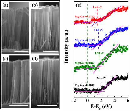
The cross section FESEM images of the grown samples as shown in Fig.1, reveal the formation of well aligned uniform NRs with high quality single crystallinityNayak et al. (2018). A thorough discussion on their structural and morphological analysis and Mg dopant concentration of these samples has been reported earlierNayak et al. (2018). The effect of Mg doping on electronic structure is characterized by XPS valence band spectra and is shown in Fig.1(e). It is well known in the literature that position of Fermi level () with respect to Valence Band Maximum () is the signature of the type and concentration of the charge carrier. We find that for sample A (undoped), is at 2.05 eV above indicating native n-type character of pristine GaN NRs as expected in GaN growth. Upon Mg incorporation in the NRs the Fermi level moves towards VBM and the reduces to 1.68, 1.60 and 1.41 eV for samples B, C and D, respectively. This clearly shows that the native n-type character is being compensated upon Mg doping.

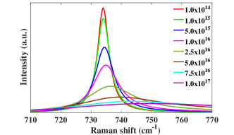
We acquired Raman spectra of all the four samples at RT and are shown in Fig. 2. Presence of E2(high) and E2(low) at and (not shown here), E1(TO) and A1(TO) at and at , respectively, confirms single crystalline wurtzite phase of the GaN films. Along with the expected peaks from GaN, a local vibrational mode (LVM) appears at 662 cm-1 for Mg doped samples, which is attributed to the Mg-N bondKaschner et al. (1999). For single crystalline and relaxed thin films, the A1(LO) and E1 (LO) phonon frequencies are reported to be 734 and 741 , respectively Davydov et al. (1998) with a deviation of 1-2 Azuhata et al. (1995); Siegle et al. (1997). Since in the scattering geometry only A1(LO) is allowed, the two different modes observed in our studies at and are identified as surface optical (SO) phonon peak and longitudinal phonon-plasmon (LPP+) mode, respectivelyRobins et al. (2016). The SO phonon peak is generally absent in bulk GaN films but is quiet prominent in the NRs due to the relatively large surface to volume ratio. Raman line profile of the LPP coupled mode is given by following equationsCheng et al. (2009)
| (1) |
where is Raman shift, is dielectric function and A() is of the following form
| (2) |
where
| (3) |
where C is the Faust-Henry coefficient, and represent the LO and TO phonon frequencies of phonon mode, respectively. and are the plasmon and phonon damping constants, respectively. is the plasma frequency given by following formula
| (4) |
where is the electron carrier density, is the effective mass of the electron and is the high frequency dielectric constant. The dielectric function in Eq.(1) is given by:
| (5) |
The schematic representation of Eq.1 is shown in Fig.3. The frequency of the LPP mode and its line width are dependent on carrier concentration and hence vary for samples with different carrier concentrations. Increase in the peak of Raman shift (frequency) and width of LPP mode, signifies increase in carrier density. For low carrier density the character of LPP mode is phonon like due to reduced plasmon-phonon coupling. However, with increasing carrier density the LPP peak shifts towards the higher frequency side, the intensity reduces and eventually the peak broadens due to increase in the coupling strength (see Figure 3). Cheng et al.Cheng et al. (2009) have shown, in case of ZnO NRs, the LPP phonon peak broadening and shifting towards higher frequency with an increase in carrier concentration, consistent with our observations. Ding et al.Ding et al. (2012) and Jeganathan et al.Jeganathan et al. (2009) have also reported similar behavior of LPP mode in Al-doped ZnO and Si-doped GaN, respectively.
| Sample | Mg:Ga | Peak | FWHM | |||
|---|---|---|---|---|---|---|
| Name | Position (cm-1) | (cm-1) | (cm-3) | (THz) | (THz) | |
| A | 0.0000 | 737.3 | 30.9 | 1.51017 | 300 | 0.10 |
| B | 0.0082 | 738.8 | 17.0 | 4.5 | 9 | 0.40 |
| C | 0.0113 | 738.3 | 13.0 | 3.6 | 1 | 0.40 |
| D | 0.0162 | 739.3 | 9.7 | 5.0 | 9 | 0.18 |
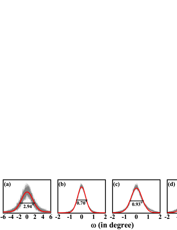
The peak position and FWHM of SO and LPP Raman modes is tabulated in Table 1, where we note that the linewidth of LPP mode is strongly influenced by Mg concentration in the films. The deconvolated Raman spectra reveal that the FWHMs of SO mode have a similar value of for all the sample under consideration (see Fig.2 (b)). We find that FWHM of LPP+ mode is significantly high () in comparison to the Mg doped ones where the FWHM varied as 17.0, 13.0 and 9.7 for sample B, C and D, respectively(see Fig.2 (b)). To make sure such changes are not due to any structural changes in the NRs samples, we carried out -scan using HR-XRD studies whose width is a signature of the crystalline quality of the films. The FWHM of the (0002) planes as obtained from -scan are noted as 2.94, 0.70, 0.93 and 0.99 for samples A, B, C and D respectively (see Fig.4). Thus, there is no direct correlation between crystal quality and peak broadening of the LPP mode. Thus, the changes in the width of line shapes of Raman spectra becomes very significant and can be used as a non-contact tool for the quantification of carrier concentration. We further fitted the deconvoluted LPP mode with Eqn.1 and the fitted plot is shown as solid lines with olive shade in Fig.2(b). The obtained values of , and from the fitted curve are tabulated in Table 1. Our estimate to the background carrier density for undoped GaN NRs sample (A) is 1.5 cm-3, which is in the same order of commonly observed carrier density in MBE grown GaN samplesRobins et al. (2016). For Mg doped samples the background n-type carrier densities are estimated to the order of cm-3 suggesting Mg incorporation has compensated the background carrier densities by two orders of magnitude. It is to note that for lightly doped sample B and C the background carrier density are 4.5 and 3.6 cm-3 respectively whereas the background carrier density of D, which has relatively higher Mg concentration than B and C, is 5 cm-3 . At this stage we hypothesize that it could be the consequence of self-compensation effect of the heavily Mg-doped GaN.
The E2(high) mode, being non-polar in nature, can be used as a measure of the inherent strain of the material. The FWHM of this mode reflects defect incorporation in the film, since strain gradient or phonon-defect scattering can lead to the broadening of this mode. We find a small change in the position of E2 (high) peak (from 567.35 to 567.39 cm-1) which suggests that a very small macroscopic strain is being generated in the NRs with Mg incorporation. We also find that with the increase in Mg-flux, FWHM of E2 (high) peak increases, which can be attributed to the generation of different kinds of point defects in the samples, depending on the concentration of Mg incorporation Kirste et al. (2013).
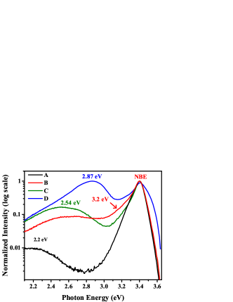
The origin of the native -type behavior of GaN is still ambiguous in the literature. Defects such as N vacancies (VN) Boguslawski et al. (1995) and Oxygen substitution (ON) Van De Walle and Neugebauer (2004) are reported as the major source of such auto-doping in GaN. Theoretical calculations based on first-principles method further suggest that Oxygen substitution in the form of is energetically more favorable. Neugebauer and Van de Walle (1996). Our previous workNayak et al. (2017a) further suggests that defect formation energy of the VN at the surface is much less than in the bulk and thus VN is a major point defect in nanostructured GaN due to it’s higher surface to volume ratioNayak et al. (2017a). Luminescence spectra recorded for sample A (undoped) shows a near band edge (NBE) peak at 3.4 eV and a broad YL at 2.20 eV (see Fig.5). However recent theoretical calculations show that VN and carbon related defects may give rise to energy states in the bandgap responsible for yellow luminescence (YL) in PL spectra of n-GaN, whereas does not Reshchikov et al. (2018). Thus, n-type and YL together suggest that VN is the dominant defect type in this case. This speculation is further backed by the luminescence spectra obtained from sample B and C (moderately doped ones), wherein a green luminescence (GL) peak is observed at 2.54 eV along with NBE and a donor acceptor pair (DAP) transition at 3.2 eV (see Fig.5). The 3.2 eV luminescence peak is the consequence of the formation of the substitutional Mg in GaN (MgGa). Reshshikov et al. Reshchikov et al. (2014) studied the defects in Mg doped GaN and suggested that most energetically favorable point defect is VN and it gives rise to green luminescence, while defect complex results in red bandsReshchikov et al. (2014). Our experimental PL data shows only GL band and a DAP transition at 3.2 eV (sample B and C) thus confirming the formation of isolated VN and in Mg doped GaN NRs. Each isolated VN results in one electron per vacancy, while may results into a free hole. Thus, formation of individual VN and , will not result in any change in carrier concentration. SIMS measurementsNayak et al. (2018) on these samples reveal Mg concentrations of 4.9, 6.0 and 2.9 atoms cm-3 and the reduction in background carrier density () with the increase in Mg concentration suggesting that VN concentration is less than 4.9 cm-3 in these samples. The compensation effect observed here is due to formation of isolated which compensates the native n-type character caused by formation of isolated VN in unintentionally n-doped GaN.
In previous sections, we envisage that the higher value of background native -type carrier density in heavily Mg-doped sample D in comparison to B and C is due to the self-compensation effect, is further strengthened by the appearance of blue luminescence (BL) in PL spectra of sample D. In past we have identified that the BL is a signature of formation of the point defect complex MgGa+Mgi and a n-type dopant to Mg-doped GaNNayak et al. (2017b).
In summary, we have grown Mg doped GaN NRs on Si (111) surface and studied the native charge compensation effect in the same using optical and X-ray photoelectron spectroscopies. Two order magnitude of native charge compensation was deduced upon Mg-doping with a concentration of 1019-1020 atoms cm-3 by analysing the line shape profile of the longitudinal plasmon-phonon coupled Raman mode. Thus we propose that line shape of the longitudinal plasmon-phonon coupled Raman mode could be a contactless method in determining the charge carrier density and the dopant induced compensation in nanostructured materials.
References
- Ihn et al. (2006) S.-G. Ihn, J.-I. Song, Y.-H. Kim, and J. Y. Lee, Appl. Phys. Lett. 89, 053106 (2006).
- Li et al. (2008) L. Li, D. Guimard, M. Rajesh, and Y. Arakawa, Appl. Phys. Lett. 92, 263105 (2008).
- Cerutti et al. (2006) L. Cerutti, J. Ristić, S. Fernández-Garrido, E. Calleja, A. Trampert, K. Ploog, S. Lazic, and J. Calleja, Appl. Phys. Lett. 88, 213114 (2006).
- Mårtensson et al. (2004) T. Mårtensson, C. P. T. Svensson, B. A. Wacaser, M. W. Larsson, W. Seifert, K. Deppert, A. Gustafsson, L. R. Wallenberg, and L. Samuelson, Nano Lett. 4, 1987 (2004).
- Glas (2006) F. Glas, Phys. Rev. B 74, 121302 (2006).
- Verheijen et al. (2006) M. A. Verheijen, G. Immink, T. de Smet, M. T. Borgström, and E. P. Bakkers, J. Am. Chem. Soc. 128, 1353 (2006).
- Lin et al. (2010) H.-W. Lin, Y.-J. Lu, H.-Y. Chen, H.-M. Lee, , and S. Gwo, Appl. Phys. Lett. 97, 073101 (2010).
- Bengoechea-Encabo et al. (2014) A. Bengoechea-Encabo, S. Albert, D. Lopez-Romero, P. Lefebvre, F. Barbagini, A. Torres-Pardo, J. M. González-Calbet, M. A. Sanchez-Garcia, and E. Calleja, Nanotechnology 25, 435203 (2014).
- Wang et al. (2008) C.-Y. Wang, L.-Y. Chen, C.-P. Chen, Y.-W. Cheng, M.-Y. Ke, M.-Y. Hsieh, H.-M. Wu, L.-H. Peng, and J. Huang, Opt. Express 16, 10549 (2008).
- Nguyen et al. (2011) H. P. T. Nguyen, S. Zhang, K. Cui, X. Han, S. Fathololoumi, M. Couillard, G. Botton, and Z. Mi, Nano Lett. 11, 1919 (2011).
- Wang et al. (2014) Q. Wang, X. Liu, M. Kibria, S. Zhao, H. Nguyen, K. Li, Z. Mi, T. Gonzalez, and M. Andrews, Nanoscale 6, 9970 (2014).
- Nayak et al. (2018) S. Nayak, R. Kumar, N. Pandey, K. Nagaraja, M. Gupta, and S. Shivaprasad, J. Appl. Phys. 123, 135303 (2018).
- Kaschner et al. (1999) A. Kaschner, H. Siegle, G. Kaczmarczyk, M. Straßburg, A. Hoffmann, C. Thomsen, U. Birkle, S. Einfeldt, and D. Hommel, Appl. Phys. Lett. 74, 3281 (1999).
- Davydov et al. (1998) V. Y. Davydov, Y. E. Kitaev, I. Goncharuk, A. Smirnov, J. Graul, O. Semchinova, D. Uffmann, M. Smirnov, A. Mirgorodsky, and R. Evarestov, Phys. Rev. B 58, 12899 (1998).
- Azuhata et al. (1995) T. Azuhata, T. Sota, K. Suzuki, and S. Nakamura, J. Phys. Condens. Matter 7, L129 (1995).
- Siegle et al. (1997) H. Siegle, G. Kaczmarczyk, L. Filippidis, A. Litvinchuk, A. Hoffmann, and C. Thomsen, Phys. Rev. B 55, 7000 (1997).
- Robins et al. (2016) L. H. Robins, E. Horneber, N. A. Sanford, K. A. Bertness, M. Brubaker, and J. Schlager, J. Appl. Phys. 120, 124313 (2016).
- Cheng et al. (2009) A.-J. Cheng, Y. Tzeng, H. Xu, S. Alur, Y. Wang, M. Park, T.-h. Wu, C. Shannon, D.-J. Kim, and D. Wang, J. Appl. Phys. 105, 073104 (2009).
- Ding et al. (2012) K. Ding, Q. Hu, W. Lin, J. Huang, and F. Huang, Appl. Phys. Lett. 101, 031908 (2012).
- Jeganathan et al. (2009) K. Jeganathan, R. Debnath, R. Meijers, T. Stoica, R. Calarco, D. Grützmacher, and H. Lüth, J. Appl. Phys. 105, 123707 (2009).
- Harima (2002) H. Harima, J. Phys. Condens. Matter 14, R967 (2002).
- Suzuki et al. (1995) M. Suzuki, T. Uenoyama, and A. Yanase, Phys. Rev. B 52, 8132 (1995).
- Melentev et al. (2016) G. Melentev, D. Y. Yaichnikov, V. Shalygin, M. Y. Vinnichenko, L. Vorobjev, D. Firsov, L. Riuttanen, and S. Suihkonen, in J. Phys. Conf. Ser (IOP Publishing, 2016), vol. 690, p. 012005.
- Kirste et al. (2013) R. Kirste, M. P. Hoffmann, J. Tweedie, Z. Bryan, G. Callsen, T. Kure, C. Nenstiel, M. R. Wagner, R. Collazo, A. Hoffmann, et al., J. Appl. Phys. 113, 103504 (2013).
- Boguslawski et al. (1995) P. Boguslawski, E. L. Briggs, and J. Bernholc, Phys. Rev. B 51, 17255 (1995).
- Van De Walle and Neugebauer (2004) C. G. Van De Walle and J. Neugebauer, J. Appl. Phys. 95, 3851 (2004).
- Neugebauer and Van de Walle (1996) J. Neugebauer and C. G. Van de Walle, Appl. Phys. Lett. 69, 503 (1996).
- Reshchikov et al. (2018) M. Reshchikov, N. Albarakati, M. Monavarian, V. Avrutin, and H. Morkoc, J. Appl. Phys. 123, 161520 (2018).
- Nayak et al. (2017a) S. Nayak, M. H. Naik, M. Jain, U. Waghmare, and S. Shivaprasad, arXiv preprint arXiv:1710.05670 (2017a).
- Reshchikov et al. (2014) M. A. Reshchikov, D. Demchenko, J. McNamara, S. Fernández-Garrido, and R. Calarco, Phys. Rev. B 90, 035207 (2014).
- Nayak et al. (2017b) S. Nayak, M. Gupta, U. V. Waghmare, and S. Shivaprasad, arXiv preprint arXiv:1708.04036 (2017b).