Pseudodoping of Metallic Two-Dimensional Materials by The Supporting Substrates
Abstract
We demonstrate how hybridization between a two-dimensional material and its substrate can lead to an apparent heavy doping, using the example of monolayer \ceTaS2 grown on Au(111). Combining ab-initio calculations, scanning tunneling spectroscopy experiments and a generic model, we show that strong changes in Fermi areas can arise with much smaller actual charge transfer. This mechanism, which we refer to as pseudodoping, is a generic effect for metallic two-dimensional materials which are either adsorbed to metallic substrates or embedded in vertical heterostructures. It explains the apparent heavy doping of \ceTaS2 on Au(111) observed in photoemission spectroscopy and spectroscopic signatures in scanning tunneling spectroscopy. Pseudodoping is associated with non-linear energy-dependent shifts of electronic spectra, which our scanning tunneling spectroscopy experiments reveal for clean and defective \ceTaS2 monolayer on Au(111). The influence of pseudodoping on the formation of charge ordered, magnetic, or superconducting states is analyzed.
I Introduction
The family of two-dimensional (2d) materials has been expanding from graphene type materials to compounds such as 2d oxides, chalcogenides and halidesNovoselov et al. (2005, 2016); Miro et al. (2014). While most of the initial research concentrated on graphene and 2d semiconductors, monolayers of metallic 2d materials, particularly transition metal mono- and dichcalcogenides such as \ceFeX (X=Se, Te)Qing-Yan et al. (2012); Ge et al. (2014); He et al. (2014); Manna et al. (2017) and \ceMX2 (M=V, Nb, Ta; X=S, Se)Xi et al. (2015); Yu et al. (2015); Cao et al. (2015); Ugeda et al. (2016); Sanders et al. (2016), can now be synthesized, processed and even integrated into van der Waals heterostructuresNovoselov et al. (2016). A central reason for the growing interest in metallic 2d systems is that they host highly intriguing many-body states including competing superconducting, nematic, magnetic, excitonic, and charge ordered phases Qing-Yan et al. (2012); Ge et al. (2014); He et al. (2014); Manna et al. (2017); Xi et al. (2015); Yu et al. (2015); Cao et al. (2015); Ugeda et al. (2016).
Generally, the electronic phase diagrams of these materials depend on carrier concentrations. Hence, one particularly important way of controlling many-electron phenomena in 2d materials is doping. It allows to switch, for instance, between insulating, charge-ordered, spin-ordered, or superconducting states of a material Lee et al. (2006); Taniguchi et al. (2012); Ye et al. (2012); Yu et al. (2015); Costanzo et al. (2016). There is however a problem in many systems: changes to electronic states (e.g. switching the prototypical material of 1T-\ceTaS2 from a Mott insulator to a superconductorYu et al. (2015)) often require electron or hole doping on the order of a few 10 of an electron or hole per unit cell Taniguchi et al. (2012); Ye et al. (2012); Yu et al. (2015); Costanzo et al. (2016). This translates into carrier concentrations cm-2 which are out of reach for gating in standard field effect transistor geometries but require ionic liquids or chemical means like atom substitution, intercalation etc. Doping at this level is potentially related to severe chemical changes of the material and substantial disorder Jeong et al. (2013).
In this letter, we discuss an alternative doping mechanism for metallic 2d materials. This mechanism, which we refer to as “pseudodoping”, is associated with considerable changes in apparent Fermi areas but much smaller actual charge transfer between substrate and 2d material. The reason why a changed Fermi area does not necessarily imply charge transfer is that the Fermi contour is made up from hybridized states of the 2d material and the substrate. We illustrate that pseudodoping of more than 10 of an electron or hole per unit cell is possible using the example of monolayer 1H-\ceTaS2 on Au(111), which has been recently studied by photoemission spectroscopySanders et al. (2016). Pseudodoping induced shifts of electronic states are often non-linearly energy-dependent such that they can affect states below and above the Fermi energy differently. In this way, pseudodoping gives a unified explanation of photoemission spectroscopy experimentsSanders et al. (2016) and scanning tunneling spectra of \ceTaS2 monolayers on Au(111). Afterwards the generic pseudodoping mechanism is explained within a simple two-band model, which we also use to discuss the influence of pseudodoping on the emergence of charge, magnetic, or superconducting order.
II Pseudodoping of \ceTaS2 on Au(111)
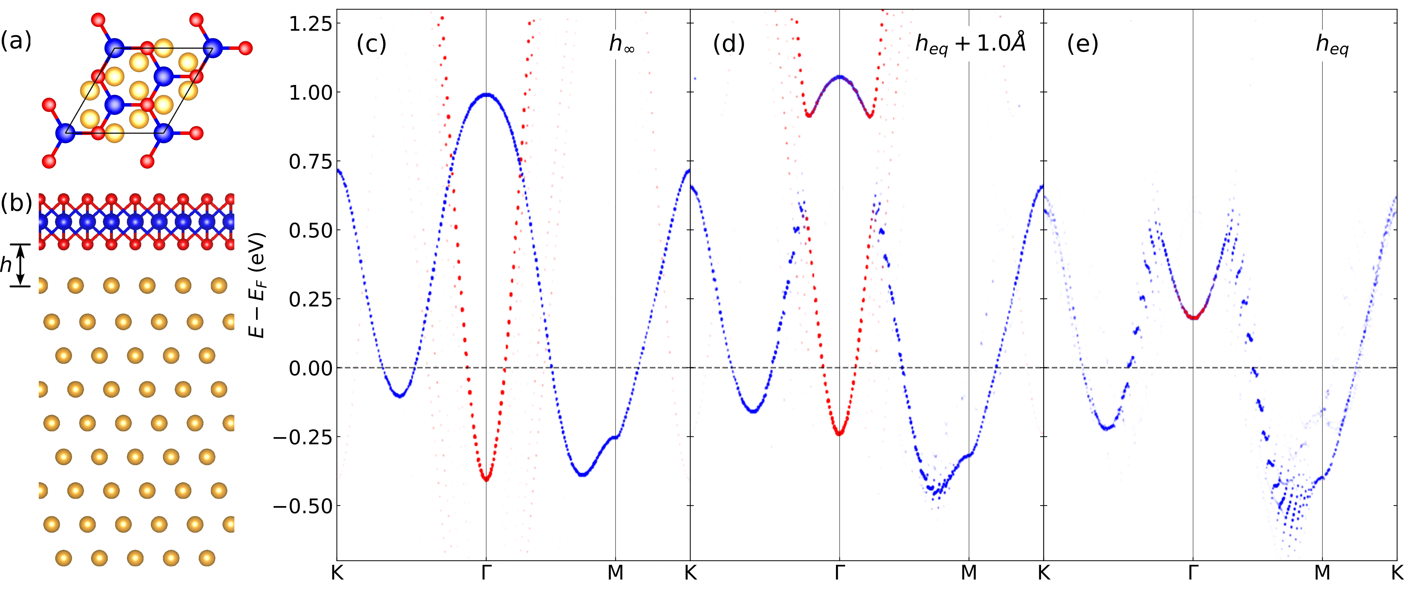
To study the interaction of 1H-\ceTaS2 monolayer and the Au substrate we performed density functional theory (DFT) calculations and scanning tunneling spectroscopy experiments. For the DFT simulations (see methods section for details), we constructed a R \ceTaS2 supercell on a supercell of the Au(111) surface, where the Au surface has been laterally compressed by 0.5 to have a commensurate structure. [See Fig.1(a) and (b).] The adsorption height of \ceTaS2 above the Au(111) surface as denoted here by the vertical distance between the lowest S atoms and the upmost Au atoms has been optimized yielding the equilibrium distance Å, which is indicative of physisorptive coupling between the \ceTaS2 and the substrate.
The influence of the coupling between the \ceTaS2 and the substrate on the electronic structure can be inferred from band structures in Fig.1(c) to (e), where the \ceTaS2 layer approaches the Au(111) surface from , i.e. the limit of a clean Au(111) substrate and a free-standing \ceTaS2 monolayer, via Å to . Unfolded band structuresMedeiros et al. (2014, 2015) of the supercell to the Brillouin zone (BZ) of the \ceTaS2 primitive cell are shown, where we highlight states with Ta- character as blue dots. It can be seen that the Ta- spectral weight of the adsorbed \ceTaS2 at Å [Fig.1(d)] and [Fig.1(e)] roughly follows the energy dispersion of the free-standing \ceTaS2 -bands [Fig.1(c)] for most parts of the BZ path, particularly below the Fermi level. The spectral weight from the upmost Au atoms (red dots) results from a Shockley-type surface state with parabolic dispersion. However, there are also some prominent changes in the electronic dispersion of system, as \ceTaS2 gradually approaches its substrate:
First, the Au- derived band at the point moves from eV below the Fermi energy () to eV above the and thus gets depopulated for a decreasing adsorption height. Such energy shifts of surface states are quite typical for noble metal substratesForster et al. (2008); Kowalczyk et al. (2008). In contrast, the Ta- derived band is lowered in energy by about 0.1 eV in the large parts of the BZ path for when compared to the free-standing case. This shift applies in particular to the \ceTa- states at and below the Fermi level and translates via the density of states (DOS) eV-1 into an apparent doping on the order of 0.2 electrons per \ceTaS2 unit cell. This amount of doping appears unusual given that \ceTaS2 is merely physisorbed on Au(111) but it is in agreement with the experiments: our calculated band structures at [Fig.1(e)] well reproduce the occupied part of the energy dispersion measured by angle-resolved photoemission spectroscopy (ARPES) in Ref. Sanders et al., 2016. Summarizing, DFT and ARPES yield an apparent doping of electrons per unit cell but the physical mechanism behind it is so far unclear.
A charge transfer (given in electrons per unit cell) over an effective distance is associated with an electrostatic potential difference , where eV/Å and Å2 is the area of the \ceTaS2 unit cell. Even if we assume that the effective distance between the charges in the 2d monolayer and the substrate is Å, i.e. much smaller than the typical distances of Å from the center of the \ceTaS2 layer to the upmost substrate atoms, a charge transfer of 0.2 would translate into a potential energy difference of eV. Comparing the work functions of \ceTaS2, eV Shimada et al. (1994) and Au(111), eVMichaelson (1977), it is clear that potential energy differences on the order of eV are unexpected. Indeed, estimates for the charge transfer based on work function differences Giovannetti et al. (2008); Khomyakov et al. (2009) generally arrive at per unit cell for substrates like Au.
We argue in the following that metallic 2d materials are instead prone to “pseudodoping” with substrate induced changes in Fermi areas, which do not primarily relate to charge transfer but rather to hybridization in a regime which is special to physisorbed 2d materials. To arrive at this conclusion, it is insightful to analyze also the unoccupied part of the electronic structure of the adsorbed \ceTaS2, Fig.1(c) to (e). In contrast to the almost rigid downward shift of the \ceTaS2 derived bands below the , we find strongly momentum and energy dependent changes in the electronic dispersion above the . In particular, avoided crossings between the Au surface state and the \ceTaS2 states strongly reshape the unoccupied part of the band structure near , which indicates significant hybridization between the substrate and \ceTaS2 layer.
III Scanning tunneling spectroscopy
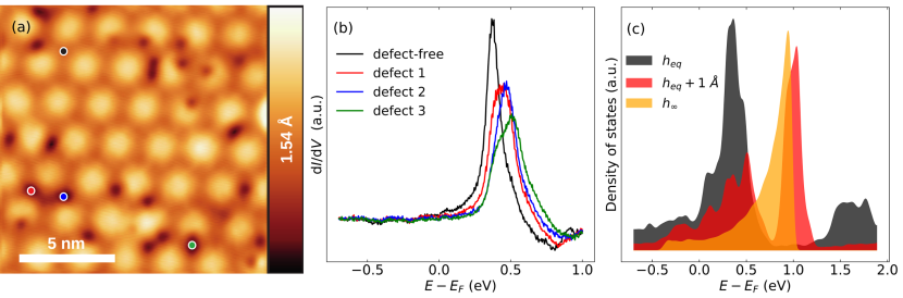
While ARPES confirms the apparent electron doping of the filled state bands, we utilize scanning tunneling microscopy/spectroscopy (STM/STS) to probe the empty state density of states. The measurements were conducted with an Omicron LT-STM operated at 5K. The base pressure was better than mbar. An electrochemically etched tungsten wire, flashed in situ, was used as the tip. The bias was applied to the sample. Topography images were taken in constant-current mode. Spectroscopy was performed utilizing a lock-in technique and the differential conductance was recorded with a modulation voltage of mV at a frequency of Hz. The sample was prepared as discussed in a previous paperSanders et al. (2016). Fig 2(a) shows the morphology of 1H-\ceTaS2 measured by STM. STS was taken at various points within the moiré unit cell of the surface, near and far away from apparent point defects. Previous studies of point defects in \ceMoS2/Au(111) indicate that such point defects arise from layer-dependent sulfur vacancies within the filmKrane et al. (2016, 2018). We observe a non-dispersing state at 0.4 eV, which shifts in proximity of various defects.
To interpret these spectra, it is insightful to compare them to DFT-simulated STS [Fig. 2(c)], where we calculated the DOS inside a sphere at 5.0 Å above the upmost S atoms of \ceTaS2 for different seperations between the \ceTaS2 and the Au(111) substrate. As shown in Fig. 2(c), for the main peak appears near 0.9 eV above the . As decreases, the peak is split into two parts due to the increasing hybridization between the Ta- band and the Au(111) surface state. I.e. the peak splitting in the simulated STS directly reflects the avoided crossing between the two aforementioned bands visible in Fig. 1 (c)-(e). The lower part of the split peak in the simulated STS eventually shifts to about 0.4 eV above the for , which is in line with the STS spectrum at the site without defects [Fig. 2(b)]. Indeed, the simulated spectrum at well accounts for the measured spectrum at the site without defects, while the calculated spectrum for the free-standing case () deviates clearly from this STS spectrum. These findings in the defect-free case represent a first experimental observation of the theoretically predicted hybridization effect.
Additional information about the interaction between the \ceTaS2 and the substrate can be obtained by inspecting STS spectra collected in the vicinity of structural defects. Those spectra are also shown in Fig. 2(b). The presence of the defects shifts the peak in STS spectrum to higher energies and reduces its amplitude with respect to the spectrum without defects [Fig. 2(b)]. Interestingly, those defect-induced changes are similar to the modifications that we find in the calculated spectra, when increasing the adsorption height from to Å [Fig. 2(c)]. Although the exact atomistic nature of the defects in the experiment is unknown, it appears that the defects can induce a local potential variation and change the vertical coupling strength of the interface. This can induce an energy shift of the surface state of Au substrateKowalczyk et al. (2008), which is qualitatively similar to the effect of changing adsorption heights. It is thus understandable that the defect-induced changes in the measured tunneling spectra [Fig. 2(b)] are very similar to the simulated spectra [Fig. 2(c)] with variations in the adsorption height and resulting changes in the hybridization strength.
Taken together, the STS experiments confirm the significant impact of the hybridization on the electronic structure of the adsorbed \ceTaS2. We argue in the following that this hybridization provides the key to understanding the apparent heavy doping of the \ceTaS2 monolayer on the Au(111) substrate in such a way that the nominal occupancy of the \ceTaS2 states varies considerably, while keeping the actual amount of charge in \ceTaS2 orbitals almost the same as in the free-standing layer.
IV Minimal model of pseudodoping
We consider a minimal model involving two bands derived from the orbital of the 2d material and of substrate, where we assume a (real valued) hybridization and a constant offset in the on-site energies between the two. The resulting Hamiltonian reads
| (1) |
where we used the Pauli matrices and summarized all -dependence of the initial dispersion in . The eigenstates of the full Hamiltonian are
| (2) |
with and corresponding energies
| (3) |
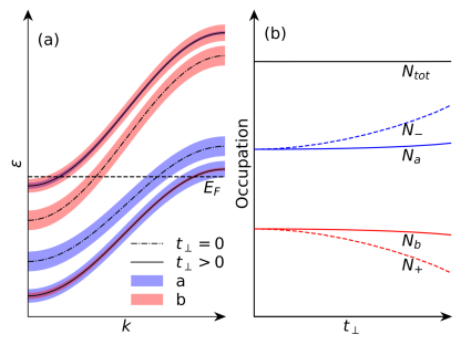
As shown in Fig. 3(a), the hybridization yields an admixture of substrate derived states to the 2d material states and vice versa as well as a level repulsion between the hybridizing bands.
With , the ground state density matrix reads
| (4) |
The central point is now to contrast the occupation of the bands
| (5) |
with the occupation of the orbitals
| (6) |
The ‘nominal’ band occupations are those measured in ARPES. In contrast, the orbital occupations and correspond to the actual charges in the 2d layer and the substrate, respectively, manifest in core level spectroscopies and also determine electric fields at the interface. Here, we have and .
For vanishing hybridization () the orbital occupancies simply coincide with the band occupancies:
where is the DOS associated with the dispersion . At finite the band fillings become
| (7) |
I.e. in ARPES experiments, the upper (lower) band appears hole (electron) doped by an amount of [c.f. dashed lines in Fig. 3(b)].
However, the occupancy of the orbital in the 2d layer is
| (8) |
Analogously, we find to second order in [c.f. solid lines in Fig. 3(b)]. I.e. the actual charge transfer cancels to leading order in while the ‘nominal’ doping does not. This is the key point of the pseudodoping mechanism. The hybridization, as depicted in Fig. 3, allows the occupancies of the lower band mainly contributed by the 2d material states to vary considerably, while keeping the actual amount of charge in the 2d material almost the same as in its free-standing form.
V Pseudodoping and electronic instabilities
Interaction terms like Coulomb interactions naturally couple localized states. In the example of a Hubbard type interaction they are of the form
| (9) |
where refers to the lattice site of the electrons in the 2d layer, to their spin and are the corresponding occupation number operators. is the on-site interaction matrix element and can describe repulsive () or attractive interaction ().
We assume that the substrate states are non-interacting and that their DOS at the Fermi level is small as compared to the DOS of the 2d material. Then, the admixture of the substrate states to the bands of the 2d material upon hybridization reduces the effective interaction inside the hybridized band by a factor of , i.e. .
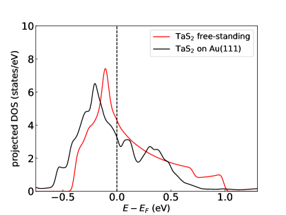
For weak coupling instabilities such as BCS superconductivity, characteristic transition temperatures are determined by the interaction and DOS at the resulting from the hybridized band. If the DOS of the original 2d band is structureless, we expect simply a reduction of . An analogous line of argumentation holds for weak coupling charge- or spin-density wave instabilities at some wave vector , where the susceptibility plays the role of an effective density of states. Thus, hybridization effects should quench tendencies towards weak coupling electronic instabilities, if the DOS / generalized susceptibilities are essentially independent of the . An even stronger suppression of instabilities is expected if or are reduced upon hybridization related pseudodoping. A comparison of the DOS of 1H-TaS2 on Au(111) and in its free-standing form (c.f. Fig. 4) shows that there is indeed a reduction of upon deposition on Au, i.e. both, the reduction of effective coupling constants and the reduced DOSAlbertini et al. (2017), will contribute here to the suppression of charge density wave / superconducting states observed in Ref. Sanders et al., 2016.
If, however, hybridization shifts a strong peak in the DOS of the 2d material’s band towards such that the hybridization induced increase in overcompensates the reduction of the effective interaction by the factor , we arrive at an increase in . Additionally, if there is a sizable interaction between electrons in the substrate states, the effective interaction can indeed be enhanced upon hybridization with the substrate, which finally also yields an increase in . Such an ‘inherited’ interaction from the substrate has been conjectured to contribute to the strongly enhanced superconducting critical temperature of FeSe when coupled to \ceSrTiO3Lee et al. (2014).
VI Conclusions
In summary, we have introduced the mechanism of “pseudodoping”, which can lead to apparent heavy doping of 2d materials on metallic substrates even in case of weak physisorption. Pseudodoping manifests itself as surprisingly large shifts of bands in ARPES experiments, as measured for \ceTaS2 on Au(111) Sanders et al. (2016). Yet, pseudodoping is expected to be ubiquitous in metallic 2d materials grown on 2d metallic substrates. It is due to hybridization of metallic 2d materials with electronic state from the supporting substrates and involves much less actual charge transfer between the layer and its substrate than changes in the Fermi areas would suggest. Nonetheless, instabilities of the electronic system towards symmetry broken states are expected to be highly sensitive to this kind of doping. Particularly, the prospect of utilizing pseudodoping to control electronic phase diagrams deserves future explorations.
Acknowledgments This work was supported by the European Graphene Flagship, by the Danish Council for Independent Research, Natural Sciences under the Sapere Aude program (Grant No. DFF-4002-00029) and by VILLUM FONDEN via the Centre of Excellence for Dirac Materials (Grant No. 11744). We acknowledge financial support from The Netherlands Organization for Scientific Research (NWO) via the VIDI project: ‘Manipulating the interplay between superconductivity and chiral magnetism at the single atom level’ with project number 680-47-534. The numerical computations were carried out on the Norddeutscher Verbund zur Förderung des Hoch- und Höchstleistungsrechnens (HLRN) cluster.
Methods: Computational Details
We performed density functional theory calculations using the Vienna Ab Initio Simulation Package (VASP) Kresse and Hafner (1994) with the projector augmented wave basis sets Blöchl (1994); Kresse and Joubert (1999) and the generalized gradient approximation to the exchange correlation potential Perdew et al. (1996). In all cases we fixed the in-plane lattice constant of 1H-\ceTaS2 to the experimental value of Å Mattheiss (1973).
The Au(111) surfaces were modeled using slabs with thickness of 30 atomic layers and a single layer of 1H-\ceTaS2 absorbed on the upper side of the slabs [see Fig. 1(a) and (b) in the main text]. The Au(111) slab was furthermore terminated with H atoms on the bottom side of the slab, i.e. on the side without \ceTaS2 coverage. The lateral coordinates of all atoms were kept fixed and we laterally compressed the Au(111) surface by to match a ()R unit cell of 1H-\ceTaS2 with a unit cell of the metal surface. The vertical coordinates of the Ta and S atoms were relaxed until forces acting on them were below 0.01 eV/Å leading to structures, where the closest vertical distance between S atoms and Au surface atoms is 2.86 Å.
References
- Novoselov et al. (2005) K. S. Novoselov, D. Jiang, F. Schedin, T. J. Booth, V. V. Khotkevich, S. V. Morozov, and A. K. Geim, PNAS 102, 10451 (2005).
- Novoselov et al. (2016) K. S. Novoselov, A. Mishchenko, A. Carvalho, and A. H. Castro Neto, Science 353 (2016).
- Miro et al. (2014) P. Miro, M. Audiffred, and T. Heine, Chem. Soc. Rev. 43, 6537 (2014).
- Qing-Yan et al. (2012) W. Qing-Yan, L. Zhi, Z. Wen-Hao, Z. Zuo-Cheng, Z. Jin-Song, L. Wei, D. Hao, O. Yun-Bo, D. Peng, C. Kai, et al., Chin. Phys. Lett. 29, 037402 (2012).
- Ge et al. (2014) J.-F. Ge, Z.-L. Liu, C. Liu, C.-L. Gao, D. Qian, Q.-K. Xue, Y. Liu, and J.-F. Jia, Nat. Mater. 14, 285 (2014).
- He et al. (2014) Q. L. He, H. Liu, M. He, Y. H. Lai, H. He, G. Wang, K. T. Law, R. Lortz, J. Wang, and I. K. Sou, Nat. Commun. 5, 4247 (2014).
- Manna et al. (2017) S. Manna, A. Kamlapure, L. Cornils, T. Hänke, E. M. J. Hedegaard, M. Bremholm, B. B. Iversen, P. Hofmann, J. Wiebe, and R. Wiesendanger, Nat. Commun. 8, 14074 (2017).
- Xi et al. (2015) X. Xi, L. Zhao, Z. Wang, H. Berger, L. Forró, J. Shan, and K. F. Mak, Nat. Nano. 10, 765 (2015).
- Yu et al. (2015) Y. Yu, F. Yang, X. F. Lu, Y. J. Yan, Y.-H. Cho, L. Ma, X. Niu, S. Kim, Y.-W. Son, D. Feng, et al., Nat. Nano. 10, 270 (2015).
- Cao et al. (2015) Y. Cao, A. Mishchenko, G. L. Yu, E. Khestanova, A. P. Rooney, E. Prestat, A. V. Kretinin, P. Blake, M. B. Shalom, C. Woods, et al., Nano Lett. 15, 4914 (2015).
- Ugeda et al. (2016) M. M. Ugeda, A. J. Bradley, Y. Zhang, S. Onishi, Y. Chen, W. Ruan, C. Ojeda-Aristizabal, H. Ryu, M. T. Edmonds, H.-Z. Tsai, et al., Nat. Phys. 12, 92 (2016).
- Sanders et al. (2016) C. E. Sanders, M. Dendzik, A. S. Ngankeu, A. Eich, A. Bruix, M. Bianchi, J. A. Miwa, B. Hammer, A. A. Khajetoorians, and P. Hofmann, Phys. Rev. B 94, 081404 (2016).
- Lee et al. (2006) P. A. Lee, N. Nagaosa, and X.-G. Wen, Rev. Mod. Phys. 78, 17 (2006).
- Taniguchi et al. (2012) K. Taniguchi, A. Matsumoto, H. Shimotani, and H. Takagi, Appl. Phys. Lett. 101, 042603 (2012).
- Ye et al. (2012) J. T. Ye, Y. J. Zhang, R. Akashi, M. S. Bahramy, R. Arita, and Y. Iwasa, Science 338, 1193 (2012).
- Costanzo et al. (2016) D. Costanzo, S. Jo, H. Berger, and A. F. Morpurgo, Nat. Nano. 11, 339 (2016).
- Jeong et al. (2013) J. Jeong, N. Aetukuri, T. Graf, T. D. Schladt, M. G. Samant, and S. S. P. Parkin, Science 339, 1402 (2013).
- Medeiros et al. (2014) P. V. C. Medeiros, S. Stafström, and J. Björk, Phys. Rev. B 89, 041407 (2014).
- Medeiros et al. (2015) P. V. C. Medeiros, S. S. Tsirkin, S. Stafström, and J. Björk, Phys. Rev. B 91, 041116 (2015).
- Forster et al. (2008) F. Forster, A. Bendounan, J. Ziroff, and F. Reinert, Phys. Rev. B 78, 161408 (2008).
- Kowalczyk et al. (2008) P. J. Kowalczyk, M. Puchalski, W. Kozłowski, P. Dąbrowski, Z. Klusek, and W. Olejniczak, Appl. Surf. Sci. 254, 4572 (2008).
- Shimada et al. (1994) T. Shimada, F. S. Ohuchi, and B. A. Parkinson, Jpn. J. Appl. Phys. 33, 2696 (1994).
- Michaelson (1977) H. B. Michaelson, J. Appl. Phys. 48, 4729 (1977).
- Giovannetti et al. (2008) G. Giovannetti, P. A. Khomyakov, G. Brocks, V. M. Karpan, J. van den Brink, and P. J. Kelly, Phys. Rev. Lett. 101, 026803 (2008).
- Khomyakov et al. (2009) P. A. Khomyakov, G. Giovannetti, P. C. Rusu, G. Brocks, J. van den Brink, and P. J. Kelly, Phys. Rev. B 79, 195425 (2009).
- Krane et al. (2016) N. Krane, C. Lotze, J. M. Läger, G. Reecht, and K. J. Franke, Nano Lett. 16, 5163 (2016).
- Krane et al. (2018) N. Krane, C. Lotze, and K. J. Franke, Surf. Sci. (2018).
- Albertini et al. (2017) O. R. Albertini, A. Y. Liu, and M. Calandra, Phys. Rev. B 95, 235121 (2017).
- Lee et al. (2014) J. J. Lee, F. T. Schmitt, R. G. Moore, S. Johnston, Y.-T. Cui, W. Li, M. Yi, Z. K. Liu, M. Hashimoto, Y. Zhang, et al., Nature 515, 245 (2014).
- Kresse and Hafner (1994) G. Kresse and J. Hafner, J. Phys.: Condes. Matter 6, 8245 (1994).
- Blöchl (1994) P. E. Blöchl, Phys. Rev. B 50, 17953 (1994).
- Kresse and Joubert (1999) G. Kresse and D. Joubert, Phys. Rev. B 59, 1758 (1999).
- Perdew et al. (1996) J. P. Perdew, K. Burke, and M. Ernzerhof, Phys. Rev. Lett. 77, 3865 (1996).
- Mattheiss (1973) L. F. Mattheiss, Phys. Rev. B 8, 3719 (1973).