Silicon Nitride MOMS Oscillator for
Room Temperature Quantum Optomechanics
Abstract
Optomechanical SiN nano-oscillators in high-finesse Fabry-Perot cavities can be used to investigate the interaction between mechanical and optical degree of freedom for ultra-sensitive metrology and fundamental quantum mechanical studies. In this work we present a nano-oscillator made of a high-stress round-shaped SiN membrane with an integrated on-chip 3D seismic filter properly designed to reduce mechanical losses. This oscillator works in the 200 kHz - 5 MHz range and features a mechanical quality factor of and a Q-frequency product in excess of Hz at room temperature, fulfilling the minimum requirement for quantum ground-state cooling of the oscillator in an optomechanical cavity. The device is obtained by MEMS DRIE bulk micromachining with a two-side silicon processing on a Silicon-On-Insulator (SOI) wafer. The microfabrication process is quite flexible and additional layers could be deposited over the SiN membrane before the DRIE steps, if required for a sensing application. Therefore, such oscillator is a promising candidate for quantum sensing applications in the context of the emerging field of Quantum Technologies.
1 Introduction
Light facilitates exploration of quantum phenomena and enables radical new technologies. Coupling light with resonant mechanical systems in an optical cavity (Fabry-Perot), known as cavity optomechanics [1, 2], serves as a basis for fundamental studies and is a flexible tool for a wide range of scientific and technological goals. We mention for instance the sensing of forces or fields at the ultimate limits imposed by quantum mechanics [3, 4], and experiments testing the foundation of physics, i.e., fixing significant constraints for the development of quantum gravity theories [5, 6].
Effects related to the quantum fluctuations of the radiation pressure are not easily detected because of classical noise sources, like the Brownian thermal noise and spurious coupling of the optomechanical system to the environment. As the number of quantum-coherent oscillations in the presence of thermal decoherence scales with the Qf product (mechanical quality factor oscillator frequency), this parameter is commonly used as a figure of merit for evaluating the oscillator’s performance in optomechanics [2]. For this reason Silicon nitride (SiN) micro- and nano-mechanical membrane resonators have attracted a lot of attention due to their exceptionally high-Q factors [7, 8]. Systems based on a membrane oscillator have shown for the first time the mechanical effect of the quantum noise in the light [9] and achieved one of the first observations of pondero-motive light squeezing [10]. Moreover, high-Q SiN membranes are interesting because they can be used in collective optotomechanics, for the realisation of entangled states between mechanical modes [11], or in systems working in the anti-squashing regime of positive feedback for enhanced sideband cooling [12].
In many cases the oscillators consist of a commercial free-standing high-stress silicon nitride (SiN) membrane supported by a silicon frame, where mechanical quality factors up to many millions can be in principle obtained [13] thanks to the large tensile stress (of the order of GPa). In these systems the mechanical loss is strongly dependent on the mounting, especially for the low frequency modes, and values randomly scattered from 104 to some 106 are usually observed [14]. Different approaches can be used to isolate the SiN membrane from its support. For instance in [11] a phononic bandgaps allowed the observation of ponderomotive squeezing at moderate cryogenic temperatures, while in [15, 16, 17] the resonating part is decoupled by its substrate by high-aspect-ratio SiN trampolines. These achievements motivate the research on customised SiN resonators for optomechanics, using MEMS wafer-scale approaches and with a precise control of the overall dissipation mechanisms [18].
In fact, the mechanical dissipation in an oscillator determines the thermal fluctuation noise, and quantum behavior can emerge only if the thermal noise force is lower than noise of quantum origin, such as radiation pressure shot-noise. The Power Spectral Density (PSD) of the thermal noise force is , where is the mass of the oscillator, its angular frequency, and the temperature. The quality factor is simply related to the fraction of mechanical energy loss per oscillation cycle, called , as: , with the energy stored in the resonant mode and the energy loss per cycle. As said above, the figure of merit which is the product of mechanical quality factor and frequency is used as object function in the device optimization process. Indeed, this figure of merit determines the number of coherent oscillations in the presence of thermal fluctuations, and the minimum requirement for room-temperature quantum optomechanics is [2].
We have recently proposed a novel coupled oscillators model for the mechanical losses in a membrane oscillator [19], considering the mutual interaction between the membrane and the frame in a recoil losses analysis. We were able to design an effective shield for the losses for all mechanical modes also in the low frequency range. In this work, we present the whole microfabrication process of a MOMS oscillator built following these design rules, where a circular SiN nanomembrane [20] is integrated on-chip with a silicon loss-shield. The shield works as isolation stage and protects the oscillator from the mechanical decoherence induced by the thermal bath. The device is fully functional from room to cryogenic temperatures, and reaches high values for all resonant modes in the measured bandwidth [0.2-5] MHz. The microfabbrication combines silicon double-side deep-RIE etching on a Silicon-On-Insulator (SOI) wafer with controlled wet-etch HF steps for removing sacrificial oxides and controlling the release of the nanomembrane. Additional layers can be deposited onto the SiN layer before fabrication, for sensing applications or to tailor the membrane reflectivity, without increasing the process complexity.
2 RESONATOR DESIGN
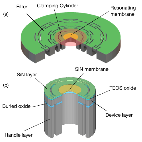
A round-shaped high-stress non-stoichiometric SiN membrane (with tensile intrinsic stress of 0.830 GPa), deposited by Low-Pressure Chemical Vapour Deposition (LPCVD), of thickness around 100 nm is analysed. This membrane interacts by the action of the radiation pressure, with a 1064 nm laser beam. To improve the quality factor and to reject vibrational noise from the environment, a mechanical filtering stage is integrated on-chip by exploiting double side Deep Reactive-Ion Etching (DRIE). A detail view of the device is shown in Fig. 1. The design of the SiN MOMS oscillator comprises of three main parts: (1) the resonating thin silicon nitride () nanomembrane, (2) the loss-shield working as intermediate filter (made of a clamping hollow cylinder and flexural/torsional springs), (3) the outer silicon frame that connects the oscillator to the sample holder. Fig. 1b shows a detailed view of the cross section of the central part of the system, highlighting the thin-film layers and the SOI wafer structure. In the subsections 2.1, 2.2, 2.3 we focus our discuss on how to minimise the thermal noise effects by reducing the mechanical dissipations of the substrate with a loss shield. In subsection 2.4 we discuss how to limit the detrimental effects on Q-fact due to the oxide layer even at liquid-He (4 K) temperatures.
2.1 Total losses
The energy loss in a SiN membrane is dominated by the intrinsic loss, that is the imaginary component in the stress-strain relation. This loss sets the ultimate limit for the mode’s -factors, but when the membrane is part of a complex device, different loss channels add up according to this simple relation:
| (1) |
where: is due to the clamping loss, describes viscous damping arising from gas surrounding the membrane, is the thermoelastic damping. We point out that, in a highly stressed membrane oscillator, the total -factor is also proportional to the internal stress. In fact when the internal stress grows, the energy dissipated in a time unit remains the same, while the oscillation frequency is much higher. The energy lost per cycle , thanks to this dilution effect, is reduced and we observe a corresponding improvement of [13, 21]. Given that the internal stress cannot be much larger than 1 GPa, the technological efforts are currently directed to reduce contributions from each loss channel.
In our MOMS device we can neglect the gas damping because the oscillator operate in a High Vacuum setup, and the thermoelastic damping of the SiN layer is orders of magnitude lower than the other losses mechanisms. Therefore the most relevant contribution is the clamping loss , that depends on the detail of the mechanical impedance of the support system. In fact, as observed for instance by Morse [22] for the case of a string supported by a sounding board, the damping depends on the mechanical impedance of the support. Only in the special case of infinitely rigid and massive support, the damping of the oscillating part is determined only by its intrinsic dissipation. In case of highly stressed membranes, the typical resonant frequency is around 1 MHz. In this frequency range, the silicon die cannot be considered as a rigid body but its full modal response must be considered in evaluating its admittance, because a support resonating at the same frequency of the membrane can be very effective in absorbing mechanical energy. For this reason we have developed a theoretical model [19] where we evaluate the loss when the membrane and support are fully-coupled, i.e. allowing for the transfer of energy in both ways. In the next section we evaluate the clamping loss when the membrane and the silicon frame are coupled structures, and we show how the loss can be reduced by using mechanical insulation stages (i.e. a loss-shield structure).
2.2 Coupled system losses
For a precise evaluation of total loss, we consider two-way energy transfer between membrane and its support. The coupling is originated from the recoil forces or torques of the structure surrounding the vibrating SiN membrane. The damping originating from recoil forces has been first evaluated by Saulson [23] in the analysis of two cascaded pendula used as mechanical filters in Gravitational Wave detectors. If we model the membrane of mass and the wafer of mass as two coupled harmonic oscillator, with and the resonant frequencies of the the uncoupled parts, the effective loss angle of the membrane in the coupled system is:
| (2) |
where are the intrinsic loss factor of the membrane and the wafer, respectively. This equation shows that in the case of a massive, rigid support with a small intrinsic dissipation (), the dissipation of the coupled system is essentially determined by the intrinsic loss in the membrane. But if the two parts are at resonance, i.e. , an approximated solution, valid for the case , and , gives:
| (3) |
and we see that the loss of the coupled membrane will grow as some mechanical energy leaks toward the supporting wafer.
2.3 Shielding recoil losses
To overcome the loss due to the coupling between the wafer and the resonating membrane, we introduce a third body with a known dynamical impedance (loss-shield stage) that can effectively decouple the membrane from the support. This intermediate stage is also effective in filtering-out low frequency displacement noise. This approach will make the -factor independent from the internal resonant modes of the system setup. In contrast, commercial TMAH/KOH wet-etched SiN membranes have a -factor dependent on the specific clamping implemented in the setup.
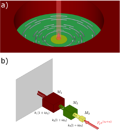
Given that a dissipative system does not admit a rigorous description in terms of normal modes [24], we evaluate by a numerical analysis the mechanical susceptibility and the associated loss of the motion of the membrane as seen from the readout port. In our system the optical readout samples the displacement of the surface on a circular area with a gaussian intensity profile centered on the membrane, as shown in Fig. 2a. We point out that the results of the analysis are only slightly dependent on the implementation details, and the optimization remains valid if the beam shape is changed or if a radio frequency readout is used.
In Fig. 2 we show a CAD image of the 3D real system, a practical implementation of a loss-shield made of flexural and torsional joints and the corresponding three-mode lumped resonating system. In both cases we indicate the application point of the laser beam used for the detection of the displacement.
As a first step, we calculated the mechanical response of the lumped tree-mode oscillator, driven by a harmonic force. The effective loss (and therefore the quality factor) is evaluated from the imaginary part of the complex susceptibility. The parameters of the model are then optimized to obtain -factors of the order of . As a second step, we study the 3D model by Finite Element and tune its geometry to match the dynamic admittance of the optimal three-oscillator model.
Referring to Fig. 2b, in the frequency domain the displacement array is related to the force array by a 33 mechanical impedance matrix as: , where is the displacement vector and is the driving force vector. The tridiagonal matrix can be easily obtained as a function of the complex spring constants (with the spring constant and the associated loss factor):
| (4) |
Here are the effective mass and the complex spring constant of the support (wafer + OFHC copper support), are the effective mass and the complex spring constant of the loss-shield structure and are the effective mass and the complex spring constant of the membrane. The formal solution of the dynamical equation is , where is the admittance matrix of the system. This equation could be solved to evaluate the resonant frequencies and the complex normal modes of the system, but on a practical level we need the response of the membrane to a single external force , as the membrane’s position is the only measured variable in the system. In agreement with the fluctuation-dissipation theorem, this is equivalent to the study of the thermal noise power spectrum of the oscillator, as seen from the readout port [25]:
| (5) |
This curve has a peak at the resonant frequency of the membrane oscillator, and the full width at half maximum of this peak gives a measurement of the quality factor. We point out that this approach estimates the quality factor measured by the dynamical response of the “coupled membrane” (i.e. the membrane coupled to its support system), that is the experimentally accessible quantity. Given that the membrane is only weakly coupled with its support, its admittance will remain similar in shape to the uncoupled oscillator case:
| (6) |
with some proper values of effective mass , effective frequency and effective loss . These effective values depend on the geometrical parameters of the loss shield and wafer, and . Numerical evaluation show that the corrections to the membrane mass and resonant frequency are negligible ( and ), while the quality factor can become smaller than the uncoupled if the frequency of the wafer approaches . In this case the loss shield turns out to be very effective in protecting the quality factor of the membrane from excessive reduction.
The optimal parameters of the loss shield, shown in Table 1 have been found with a numerical approach based on the model of Fig. 2b [19]. The actual geometry consistent with these parameters has been developed with the help of FEM modelling.
| 3-oscillator model | |
|---|---|
2.4 Intrinsic losses
A critical issue concerning the design of MOMS oscillator is the thin oxide layer that is used as etch-stop layer for the Deep-RIE on the back side. The thin TEOS layer is shown in the design concept of the oscillator Figure 1. This layer is completely removed from the membrane in a release step following the Deep-Rie etching of the substrate. This layer, if not removed properly at the membrane’s edge, can originate an additional loss depending on its thickness. In particular, the dissipation behaviours of this layer can be critical at cryogenic temperatures, commonly required in quantum optomechanics, as has a dissipation peak at 50 K [26] that affects its behaviour down to Liquid Helium temperatures.
| Low temperature | Room temperature | |
|---|---|---|
| () | () | |
| (GPa) | 77 | 77 |
| (GPa) | 260 | 260 |
| 2800 | 2800 | |
| 2100 | 2100 | |
| 800 | 800 | |
| (TL) | ||
The intrinsic quality factor () of a free-standing membrane dominated by intrinsic stress can be calculated, for a square-shaped membrane, with the approach described in [21] :
| (7) |
where are the mode indexes, with the flexural rigidity, the thickness and the side length of the square-shaped SiN layer. and are the real and imaginary parts of the complex Young’s modulus, that are related to the loss factor according to the following relation: . We take 7 as an estimate for the quality factor in the case of a circular membrane with similar frequency.
In 7, the physical meaning of is the ratio between the bending energy to the elongation energy for the fundamental mode (in our case ). The loss at the edge is described by the term independent from the mode indexes , that is:
| (8) |
To evaluate the lower limit of the quality factor due to the TEOS oxide layer, we estimate the components of the complex Young modulus by considering the effective thin film layer:
| (9) | |||
| (10) |
where and are the effective real and imaginary Young modulus, are the volume fractions while are the Young modulus and the loss angle , as reported in Table 2.
These data are used to simulate the total membrane loss by FEM, showing that for a system without oxide the Q-factor can potentially reach at 4 K, while a reduction of the overall Q-factor is expected in the bilayer sistem (100/290) nm. At room temperature the extra dissipation due to the layer is negligible. Results at 4 K and 300 K are reported in Figure 3.
3 MICROFABRICATION
Resonators were fabricated exploiting MEMS bulk-micromachining by Deep-Reaction Ion Etching (DRIE) and through wafer two-side processing, a process which has already demonstrated the capability of producing low-loss micro-mechanical systems [27, 28].
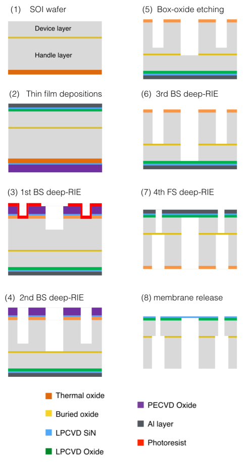
Resonators were fabricated from 4-inches Silicon-On-Insulator (SOI) Floating Zone wafer (Icemos Technology Ltd.) of total thickness (device layer 250 m), orientation with resistivity (Fig. 4 step 1). We patterned the handle and device layers by multiple DRIE etching steps, using the buried oxide as etch stop layer.
Firstly, on the device layer we deposited a multilayer thin-film stack composed of a low pressure chemical vapor deposition (LPCVD) tetraethyl orthosilicate (TEOS) oxide film with thickness (on the bottom), the 100-nm-thick LPCVD SiN membrane (in the middle) and a thick RF-sputtered pure layer (on the top) as it is shown in Fig. 4 step 2. The TEOS oxide works as etch stop layer during DRIE etching steps while the layer is used as front side mask and as protection layer for the wet/dry etching processing phases. The SiN membrane is deposited at about by tuning the stress to about (measured on a Si wafer by curvature methods TENCOR Flexus FLX-2908). Before RF-sputtering of the layer, a plasma enhanced chemical vapor deposition (PECVD) oxide mask of thickness was deposited on the back side at (Fig. 4 step 2). Silicon etching has been realized by means of DRIE two pulse BOSCH process in Omega i2L Rapier at . A multi-level etching processing was performed to obtain the membrane’s hole and the loss-shield masses, using resist AZ9260 and the nested PECVD oxide mask. With reference to Fig. 4 step 3-4 we first etch and after stripping the resist we performed a second etching step of landing on the buried-oxide.
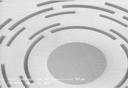
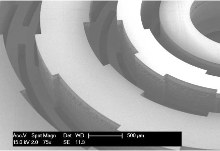
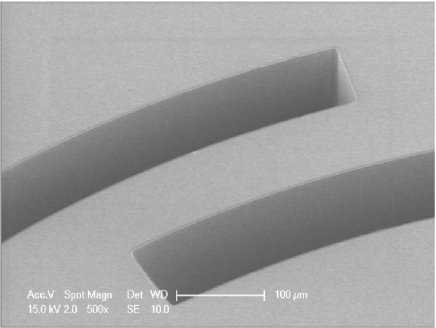
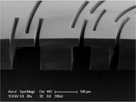
The estimated average etching rates were about m/cycle for Si and nm/cycle for the PECVD oxide. The gas-flow rate and number of cycles were optimised to control the aspect ratio dependant etching and notching. Afterwards, we removed the buried oxide by means of an HF-based solution (Fig. 4 step 5) that fully etches the PECVD oxide mask. The SiN layer on the back side works as etch stop layer for HF and protects the thermal oxide underneath. To release the thin-film stack we performed the third DRIE etching step () exploiting the thermal oxide as mask (Fig. 4 step 6). We divided the etching step in two sub-steps in order to prevent membranes failure. We saw re-entrant sidewalls due to aspect ratio dependant etching rates. By a last DRIE etching step (Fig. 4 step 7) we obtained the front-side suspending structure in the device layer; in this case we used a photoresists AZ9260 (to avoid micro masking of the Al layer). Front and back side of the whole oscillator structure are shown in Fig. 5 and Fig. 6 respectively, detailed views of the torsional-flexural joints are shown in Fig. 7 and Fig. 8.
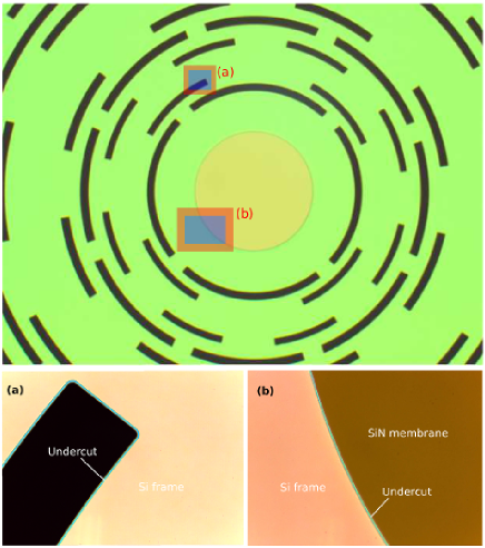
The last step is the SiN membrane release. First we stripped the Al layer using a PES solution, then by means of an HF-based solution we etched the TEOS oxide (Fig. 4 step 8). A HF over-etch is needed in this phase in order to completely release the SiN layer, as any remnant TEOS oxide layer could spoil the mechanical Q-factor of the membrane. The appearance of the undercut as it is shown in Fig. 9 (b) represents a good way to set a proper over-etching time. The process ends with dicing and cleaning from resist residues by oxygen plasma (TEPLA) and by solution .
4 EXPERIMENTAL CHARACTERISATION
The experimental set-up used for the measurement of the quality factor is shown in Fig. 10. A beam of reflected by the PBS1 from our light source, a Nd:YAG at , is aligned in a Michelson interferometer followed by a balanced homodyne detection. In details, a polarizing beam-splitter (PBS2) divides the beam into two parts, orthogonally polarized, forming the Michelson interferometer arms. At the end of the first one (reference arm) an electromagnetically-driven mirror M1 is used for phase-locking the interferometer in the condition of maximum displacement sensitivity. A double pass through a quarter-wave plate rotates by 90∘ the polarization of this beam, which is then transmitted by PBS2. The second beam (sensing arm) is focused on the membrane oscillator firmly fixed inside the vacuum chamber, and after reflection and double pass through the quarter-wave plate is reflected by the PBS2, where it overlaps with the reference beam reflected by M1.
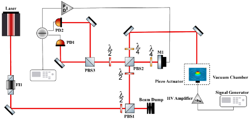
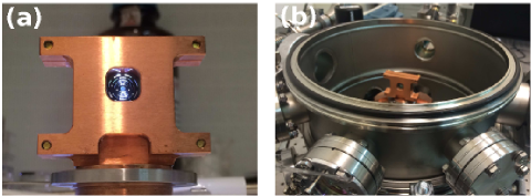
The overlapped beams are then monitored by a homodyne detection, consisting of a half-wave plate, rotating the polarizations by 45∘, and a polarizing beamsplitter (PBS3) that divides the radiation into two equal parts sent to the photodiodes PD1 and PD2, whose outputs are subtracted. The signal obtained is a null-average, sinusoidal function of the path difference in the interferometer. Such a scheme is barely sensitive to laser power fluctuations. The difference signal is used as error signal in the locking servo-loop (the locking bandwidth is about 1 kHz) and also sent to the acquisition instruments for sensing the displacement of the membrane. The quality factor of the resonant modes are evaluated by the measurement of the free decay time after resonant excitation with a piezoelectric crystal. When the drive signal is removed, the mechanical vibration follows an exponentially damped decay whose envelope amplitude varies according to: where is the decay time of the mode and is the resonance frequency of mode with indexes , as explained in the next Section. In Fig. 11(a) we show the customized clamping systems for a chip and the vacuum chamber Fig. 11(b). The clamping system is isolated from vibrations with a spring-mass system linked to the optical table from the bottom and the pressure in the vacuum chamber is about to prevent gas damping effects.
5 RESULTS AND DISCUSSION
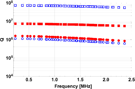
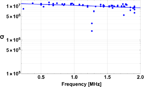
In Fig. 12 we report the quality factor of all of the frequency modes (up to 2 MHz) of a reference device (wf1726-14). In comparison with commercial devices, measured for instance in [21], these results highlight the effectiveness of the integrated loss-shield, as almost all modes achieve a high value, in good agreement with what is expected by (7) for square-shaped membranes.
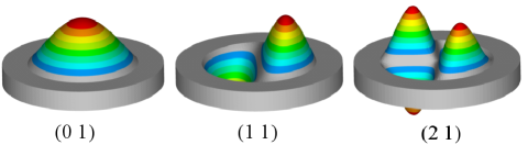
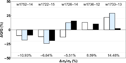
In general, microfabricated systems should ensure good reproducibility of the operating parameters. To evaluate the robustness of our microfabrication process we compare the -factor measurements for five devices obtained in five different runs. Relevant geometrical parameters related to the thin film oxide and nitride layers are reported in Table 3. In Table 4 we report the intrinsic stress , the measured diameter and the -factor measurements for three vibrational modes. From these data we estimate the sensitivity of the -factor to the variations of the intrinsic stress and undercut . The analysis refer to the three low-frequency oscillations with mode indexes , with modal shape shown in Figure 13. We point out that for these low frequencies modes a high quality factor can be obtained only thanks to the loss-shield stage.
Stress variation are originated by pressure fluctuations and small variations of the gas ratio during the LPCVD deposition. A precise estimate of the intrinsic stress of the membrane, reported in Table 4, was derived from the interferometric measurement of the frequency (Fig. 10). In fact the stress and the resonant frequency are connected by the relation: , where is the -th root of the Bessel polynomial of order and . Here is the density of the SiN film, and the diameter was directly measured on the device by Leica DM750M optical microscope with magnification of 50. According to 7, the mechanical -factor in a square membrane is directly related to the intrinsic stress by the dilution effect of the mechanical losses in SiN films. For this reason it is not surprising that higher quality factors are generally observed when the stress is higher. In Fig. 14 we show the relative variation of as a function of the relative variation of stress, taking as reference value the average of the measured stress over the five different devices.
| DEVICE | |||
|---|---|---|---|
| w1722-15 | 298 | 108 | 5.48 |
| w1726-14 | 298 | 100 | 2.35 |
| w1733-13 | 302 | 109 | 6.37 |
| w1736-12 | 302 | 109 | 2.60 |
| w1752-14 | 298 | 100 | 2.21 |
| DEVICE | Q | |||||
|---|---|---|---|---|---|---|
| 247.47 | (01) | 2.09 | ||||
| w1722-15 | 703.07 | 1.55 | 374.38 | (11) | 3.14 | |
| 568.29 | (21) | 4.42 | ||||
| 233.98 | (01) | 1.96 | ||||
| w1726-14 | 712.22 | 1.65 | 372.96 | (11) | 4.65 | |
| 499.95 | (21) | 5.56 | ||||
| 274.16 | (01) | 3.22 | ||||
| w1733-13 | 862.90 | 1.55 | 438.82 | (11) | 6.27 | |
| 718.95 | (21) | 7.06 | ||||
| 275.91 | (01) | 3.00 | ||||
| w1736-12 | 818.48 | 1.50 | 439.49 | (11) | 4.87 | |
| 589.91 | (21) | 6.25 | ||||
| 241.82 | (01) | 2.09 | ||||
| w1752-14 | 671.33 | 1.55 | 384.88 | (11) | 3.49 | |
| 516.77 | (21) | 4.50 |
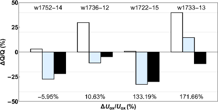
The undercut is roughly proportional to the etching time chosen for the release of the SiN membrane (Fig. 4 step 8). Actually it is used to check if the SiN membrane is fully released from the SiO2 layer underneath: no undercut means no free-standing membrane. Starting form the reference process, corrisponding to device w1726-14, different etching time were tested to check possible effects on the quality factor. For each wafer the undercut, measured with Leica DM750M using a magnification of 50, is reported in Table 3. As shown in Fig. 15, where no clear correlation can be seen, the undercut does not influence the -factor of the modes. Here the relative variations are evaluated from the reference device.
6 Conclusion
This work presents the microfabrication process for the production of high-Q SiN membranes with an integrated on-chip 3D loss-shield. Within its operating bandwidth (0-5 MHz), the device preserves the intrinsic Q-factor of the pretensioned round-shaped nanomembrane, regardless of the modal order or resonant frequency. In particular, -factors at room temperature are about , achieving the minimum requirement for room-temperature quantum optomechanics THz for all modes with frequency higher than kHz.
The device is obtained by MEMS bulk-micromachining via Deep-Reaction Ion Etching (DRIE), combined with a two-side processing on a thick SOI wafer. The microfabrication process is quite flexible and additional layers could be deposited over the SiN membrane before the DRIE steps, if required for a sensing application. Therefore, such oscillator is a promising candidate for quantum sensing applications in the context of the emerging field of Quantum Technologies.
References
- [1] I. Favero, K. Karrai, “Optomechanics of deformable optical cavities,” Nat. Photonics, vol. 3, pp. 201-205, 2009, doi:10.1038/nphoton.2009.42.
- [2] M. Aspelmeyer, T. J. Kippenberg, F. Marquardt, “Cavity optomechanics,“ Rev. Mod. Phys., vol. 86, art. no. 1391, 2014, doi: 10.1103/RevModPhys.86.1391.
- [3] M. Metcalfe, “Applications of cavity optomechanics,” Appl. Phys. Rev., vol. 1, art. 031105, 2014, doi: 10.1063/1.4896029.
- [4] A. Pontin, M. Bonaldi, A. Borrielli, L. Marconi, F. Marino, G. Pandraud, G. A. Prodi, P. M. Sarro, E. Serra, F. Marin, “Quantum nondemolition measurement of optical field fluctuations by optomechanical interaction,” Phys. Rev. A, vol. 97, art. no. 033833, 2018.
- [5] I. Pikovski, M.R. Vanner, M. Aspelmeyer, M. S. Kim, Časlav Brukner, “Probing Planck-scale physics with quantum optics,” Nature Physics, vol. 8, pp. 393-397, 2012, doi: 10.1038/nphys2262.
- [6] M. Bawaj, C. Biancofiore, M. Bonaldi, F. Bonfigli, A. Borrielli, G. Di Giuseppe et al., “Probing deformed commutators with macroscopic harmonic oscillators,“ Nat. Communications, vol. 6, art. no. 7503, 2015, doi: 10.1038/ncomms8503.
- [7] J. D. Thompson, B. M. Zwickl, A. M. Jayich, F. Marquardt, S. M. Girvin, J. G. E. Harris, “Strong dispersive coupling of a high-finesse cavity to a micromechanical membrane,” Nature, vol. 452, pp. 72-75, 2008, doi: 10.1038/nature06715
- [8] Y. Tsaturyan, A. Barg, E. S. Polzik and A. Schliesser, “Ultracoherent nanomechanical resonators via soft clamping and dissipation dilution,” Nature Nanotechnology, vol. 12, pp. 776–783, doi: 10.1038/nnano.2017.101
- [9] T. P. Purdy, R. W. Peterson, C. A. Regal, “Observation of Radiation Pressure Shot Noise on a Macroscopic Object,” Science, vol. 339, n. 6121, pp. 801-804, 2013, doi: 10.1126/science.1231282.
- [10] T. P. Purdy, P.L. Yu, R. W. Peterson, N. S. Kampel, C. A. Regal, “Strong Optomechanical Squeezing of Light,” Phys. Rev. X, vol. 3, art. no. 031012, 2013, doi: 10.1103/PhysRevX.3.031012.
- [11] W. H. P. Nielsen, Y. Tsaturyan, C.B. Møller, E.S. Polzik, A. Schliesser, “Multimode optomechanical system in the quantum regime,” PNAS, vol. 114, n. 1, pp. 62-66, 2017, doi: 10.1073/pnas.1608412114.
- [12] M. Rossi, N. Kralj, S. Zippilli, R. Natali, A. Borrielli, G. Pandraud, E. Serra, G. Di Giuseppe and D. Vitali, “Enhancing sideband cooling by feedback controlled light,” Phys. Rev. Lett., vol. 119, art. no. 123603, 2017, doi: 10.1103/PhysRevLett.119.123603.
- [13] Q. P. Unterreithmeier, T. Faust, J. P. Kotthaus, “Damping of nanomechanical resonators,” Phys. Rev. Lett., vol. 105, art.no 027205, 2010, doi: 10.1103/PhysRevLett.105.027205.
- [14] D. J. Wilson, C. A. Regal, S. B. Papp, and H. J. Kimble, “Cavity Optomechanics with Stoichiometric SiN Films,” Phys. Rev. Lett., vol 103, art. no. 207204, 2009, doi: 10.1103/PhysRevLett.103.207204.
- [15] R. A. Norte, J. P. Moura, S. Gröblacher, “Mechanical Resonators for Quantum Optomechanics Experiments at Room Temperature,” Phys. Rev. Lett., vol. 116, art. no. 147202, 2014, doi: 10.1103/PhysRevLett.116.147202.
- [16] C. Reinhardt, T. Müller, A. Bourassa, and J. C. Sankey, “Ultralow-Noise SiN Trampoline Resonators for Sensing and Optomechanics,” Phys. Rev. X, vol. 6, art. no. 021001, 2016, doi: 10.1103/PhysRevX.6.021001.
- [17] M. J. Weaver, B. Pepper, F. Luna, F. M. Buters, H. J. Eerkens, G. Welker, B. Perock, K. Heeck, S. de Man, D. Bouwmeester, “ Nested trampoline resonators for optomechanics” Appl. Phys. Lett. 108, 033501 (2016); https://doi.org/10.1063/1.4939828
- [18] L.G. Villanueva, S. Schmid, “Evidence of Surface Loss as Ubiquitous Limiting Damping Mechanism in SiN Micro- and Nanomechanical Resonators,” Phys. Rev. Lett., vol. 113, art. no. 227201, 2014, doi: 10.1103/PhysRevLett.113.227201.
- [19] A. Borrielli, L. Marconi, F. Marin, F. Marino, B. Morana, G. Pandraud, et al., “Control of recoil losses in nanomechanical SiN membrane resonators,” Phys. Rev. B, vol. 94, art. no. 121403(R), 2016, doi: 10.1103/PhysRevB.94.12140.
- [20] E. Serra, M. Bawaj, A. Borrielli, G. Di Giuseppe, S. Forte, N. Kralj, “Microfabrication of large-area circular high-stress silicon nitride membranes for optomechanical applications,” AIP Advances, vol. 6, art. no. 065004, 2016, doi: 10.1063/1.4953805.
- [21] P.-L. Yu, T. P. Purdy, C. A. Regal, “Control of Material Damping in High-Q Membrane Microresonators,” Phys. Rev. Lett., vol. 108, art. no. 083603, 2012, doi: 10.1103/PhysRevLett.108.083603
- [22] Philip M. Morse, “Vibration and Sound,” McGraw-Hill (New York, 1948), pp. 133-147.
- [23] P.R. Saulson, “Thermal Noise in Mechanical Experiments,” Phys. Rev. D, vol. 42, p. 2437, 1990, doi: 10.1103/PhysRevD.42.2437.
- [24] L. Meirovitch, Dynamics and Control of Structures (John Wiley & Sons, 1990).
- [25] Yu. Levin, “Internal thermal noise in the LIGO test masses: A direct approach,” Phys. Rev. D, vol. 57, p. 659, 1998, doi: 10.1103/PhysRevD.57.659.
- [26] X. Liu, T. H. Metcalf, Q. Wang and D. M. Photiadis, “Elastic Properties of Several Silicon Nitride Films,” Mater. Res. Soc. Symp. Proc. vol. 989, p. A22-01, 2007, doi: 10.1557/PROC-0989-A22-01.
- [27] E. Serra, A. Borrielli, F.S. Cataliotti, F. Marin, F. Marino, A. Pontin, G.A. Prodi, and M. Bonaldi, “A ”low-deformation mirror” micro-oscillator with ultra-low optical and mechanical losses,“ Appl. Phys. Lett., vol. 101, art. no. 071101, 2012, doi: 10.1063/1.4745510.
- [28] A. Borrielli, A. Pontin, F. S. Cataliotti, L. Marconi, F. Marin, F. Marino, G. Pandraud, G. A. Prodi, E. Serra, and M. Bonaldi, “Low-loss optomechanical oscillator for quantum optics experiments,” Phys. Rev. Applied, vol. 3, art. no. 054009, 2015, doi: 10.1103/PhysRevApplied.3.054009.