Molecular screening effects on exciton-carrier interactions in suspended carbon nanotubes
Abstract
Photoluminescence spectroscopy measurements are performed on suspended carbon nanotubes in a field-effect configuration, and the gate voltage dependence of photoluminescence spectra are compared for the pristine and the molecularly adsorbed states of the nanotubes. We quantify the molecular screening effect on the trion binding energies by determining the energy separation between the bright exciton and the trion emission energies for the two states. The voltage dependence shows narrower voltage regions of constant photoluminescence intensity for the adsorbed states, consistent with a reduction in the electronic bandgap due to screening effects. The charge neutrality points are found to shift after molecular adsorption, which suggests changes in the nanotube chemical potential or the contact metal work function.
The Coulomb interactions are enhanced in carbon nanotubes (CNTs) because of the limited screening in one-dimensional systems,Ogawa and Takagahara (1991); Ando (1997) which result in stable exciton and trion formation even at room temperature.Wang et al. (2005); Maultzsch et al. (2005); Matsunaga, Matsuda, and Kanemitsu (2011); Yoshida, Popert, and Kato (2016) Their optical properties are sensitive to environmental screening due to their atomically thin nature, and the dielectric environmental effects can explain the variety of emission energies observed from bundles,Fantini et al. (2004) surfactant wrapped nanotubes,Weisman and Bachilo (2003) DNA wrapped nanotubes,Heller et al. (2006) and air-suspended nanotubes.Lefebvre et al. (2004); Ohno et al. (2006)
Even for the least screened air-suspended nanotubes, the excitons are known to be affected by adsorbed molecules,Finnie, Homma, and Lefebvre (2005); Milkie et al. (2005); Homma et al. (2013); Uda, Ishii, and Kato (2018); Machiya et al. (2018) and therefore the screening effects can be further reduced when the molecules are desorbed. The spectral shifts in temperature dependenceFinnie, Homma, and Lefebvre (2005) and power dependence measurementsMilkie et al. (2005) have been attributed to heating-induced molecular desorption, while more controlled measurements have shown that water adsorption can explain the spectral changes.Homma et al. (2013) Taking advantage of the drastic shifts in the emission and absorption spectra, all-optical memory operationUda, Ishii, and Kato (2018) as well as optical control of coupling between nanobeam cavities and nanotubesMachiya et al. (2018) have been demonstrated. Excited excitonic states show even more pronounced molecular-screening induced energy shifts because of the small binding energies,Lefebvre and Finnie (2008) implying associated changes in the electronic bandgap. Such spectral changes are also expected for trion emission, whereas any modification of the bandgap should influence gate-induced charge accumulation.
Here we investigate the molecular screening effects on trion binding energies and carrier-induced photoluminescence (PL) quenching in suspended CNTs using field-effect transistor (FET) structures. Comparing the gate voltage dependent PL from nanotubes before and after molecular adsorption, we find differences in the emission energies as well as the voltage dependence. The adsorption induced changes in the emission energies indicate that trion binding energies are largely modified by the molecules. Furthermore, the unquenched voltage region for the bright exciton PL are narrower for the adsorbed state, which can be explained by a decrease in the electronic bandgap by molecular screening. We also find a shift of the charge neutrality point, which could arise from changes in the chemical potential for the nanotubes or the work function of the contact metals.
The suspended-nanotube FETsYasukochi et al. (2011); Kumamoto et al. (2014); Yoshida et al. (2014); Yoshida, Popert, and Kato (2016); Uda et al. (2016) are fabricated from -doped Si substrates with a resistivity of 0.01-0.02 cm and a 300-nm-thick oxide layer [Fig. 1(a)]. We form trenches using electron beam lithography and dry etching. Another lithography step defines the contact electrodes, and sputtering is used to deposit 1.5 nm Ti and 40 nm Pt. Catalyst areas are patterned on the electrodes with a third lithography step and chemical vapor deposition (CVD) is performed at 800∘C to grow CNTs over the trenches.Maruyama et al. (2002) Scanning electron micrograph of a typical device is shown in Fig. 1(b). We gate the nanotubes by applying a back gate voltage to the substrate while grounding the nanotube contacts.

The nanotube devices are characterized with a home-built microspectroscopy system.Ishii, Yoshida, and Kato (2015) A wavelength tunable Ti:sapphire laser is used for excitation, and the polarization is rotated using a half-wave plate. An objective lens with a numerical aperture of 0.8 and a working distance of 3.4 mm is used to focus the beam onto a nanotube. We use an excitation power of 30 W and the laser polarization is aligned parallel to the tube axis. The same objective lens is used to collect the PL from the nanotube, and the signal is detected by an InGaAs photodiode array attached to a spectrometer. All measurements are carried out at room temperature in dry nitrogen, but we note that the samples have been exposed to air during transfer from the CVD furnace to the measurement system.
Figure 1(c) shows a PL excitation map taken within few hours after taking out the sample from the CVD furnace. The emission occurs at the energy, while the resonance can be observed as a peak in the excitation energy. The and excitonic resonances appear at higher energies compared to reported values in air ambient,Lefebvre and Finnie (2007); Ishii, Yoshida, and Kato (2015) and match the energies observed for nanotubes without adsorbates.Chiashi et al. (2008); Homma et al. (2013) We will refer to this state as the “pristine” state, which is metastable and lasts up to 10 hours in air.
After sufficient time, both and resonances redshift [Fig. 1(d)] to values consistent with tabulated data for air-suspended nanotubes.Ishii, Yoshida, and Kato (2015) The shifting of the resonance energies indicate molecular adsorption,Lefebvre and Finnie (2008); Chiashi et al. (2008); Homma et al. (2013) and we thus refer to this redshifted state as the “adsorbed” state. Since the molecules can be thermally desorbedLefebvre and Finnie (2008); Xiao, Anderson, and Fraser (2014) we heat the samples to 400∘C in Ar gas with 3% H2 for 20 minutes when we need to convert the nanotubes back to the pristine state.
To investigate the effects of molecular adsorption on the interplay of carriers and excitons, we take PL spectra as a function of gate voltage for both the pristine and the adsorbed state of this nanotube (Fig. 2). Gate-induced quenching of the bright exciton emission as well as appearance of the trion emission near 0.85 eV are observed for both states,Yoshida, Popert, and Kato (2016) but emission energies are clearly redshifted for the adsorbed state. In addition, there are also subtle differences in the voltage dependence. The pristine state shows a voltage offset of about 150 mV compared to the adsorbed state, while the voltage ranges of without appreciable PL quenching are slightly different for the two states.
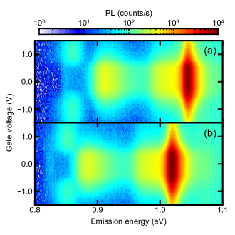
We first discuss the energy separation between the exciton peak and the trion peak. In Fig. 3(a), the emission spectra taken at V for the pristine (blue curve) and the adsorbed state (red curve) are plotted. The trion peak shows a shift by 9 meV, which is smaller than the exciton peak shift of 24 meV. As the -trion energy separation is the sum of the trion binding energy and the singlet-triplet splitting,Matsunaga, Matsuda, and Kanemitsu (2011); Santos et al. (2011); Yoshida, Popert, and Kato (2016) it is reasonable that we observe smaller for the adsorbed state since screening from the adsorbed molecules should reduce the trion binding energy.
In order to quantify the molecular screening effects on the trion binding energies, we have performed measurements on nanotubes with various chiralities. The obtained values of for both pristine and adsorbed states are plotted as a function of the nanotube diameter in Fig. 3(b). It is known that the energy separation between the and the trion peak follows the relation , where is the trion binding energy and is the singlet-triplet splitting.Matsunaga, Matsuda, and Kanemitsu (2011); Santos et al. (2011); Yoshida, Popert, and Kato (2016) For the adsorbed states, the data points coincide with the previous observationYoshida, Popert, and Kato (2016) corresponding to meVnm and meVnm2 (red curve). For the pristine states, energy separations are consistently larger than the adsorbed states by about 20 meV. Assuming that both and scale by the same factor upon molecular desorption, we fit the data by . The result is shown as a blue line in Fig. 3(b), giving . This value is comparable to the ratio of 1.10 between the exciton binding energies for the pristine state and the adsorbed state,Lefebvre and Finnie (2008) and corresponds to a reduction in the trion binding energy caused by the molecular screening of 13 meV for nm tubes.

We now turn our attention to the quenching behavior of the bright exciton emission. For the data sets in Fig. 2, we have integrated the PL intensity around the emission energies, and the gate voltage dependence of the peak area are plotted in Fig. 4(a) for the pristine (blue curve) and the adsorbed (red curve) states. Within a voltage range near V, the PL intensity is roughly constant, whereas a substantial decrease is observed beyond a threshold for both positive and negative gate voltages. As the quenching occurs due to electrostatically introduced carriers,Perebeinos and Avouris (2008); Steiner et al. (2009); Yasukochi et al. (2011) the voltage range with constant PL indicates a region with negligible carrier accumulation, while the gate voltage at the center of the constant PL region corresponds to the charge neutrality point. The voltage offset between the pristine and the adsorbed states is now clearly visible, and the difference in the width of the constant PL region can also be recognized.
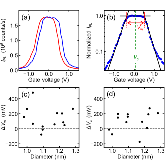
To evaluate the differences in a quantitative manner, we extract the voltage range of the constant PL region [Fig. 4(b)]. We first draw a line corresponding to the constant PL intensity by averaging all the data points above 95 % of the maximum intensity. We then take the gate voltage regions where the PL intensity is between 20 % and 70 % of the maximum, and fit the data with a line representing exponential quenching with gate voltage. Such fits are performed for both positive and negative gate voltages, and the lines are extrapolated back towards zero gate voltage to obtain the intersections with the constant intensity line. We use the positions of the intersections to determine the width of the voltage range and the center voltage for the constant PL intensity region as shown in Fig. 4(b).
We have systematically repeated such measurements and analyses on 13 tubes to acquire and for the two states, and we subtract the values for the adsorbed states from those of the pristine states to obtain the differences and to identify the molecular screening effects. In Figs. 4(c) and 4(d), we plot and , respectively, as a function of nanotube diameter. The scatter of the data points are large and there is no apparent dependence on the tube diameter, but we find that there are noticeable differences between the two states.
The width of the constant PL region is on average larger by about 140 mV for the pristine state compared to the adsorbed state [Fig. 4(c)]. This width should be correlated with the electronic bandgap, as it indicates the voltage range for which there is negligible charge accumulation.Yasukochi et al. (2011); Jiang et al. (2015) It is reasonable that the widths are narrower for the adsorbed state, since the molecular screening of the electron-electron interactions would result in a reduction of the electronic bandgap.Ando (1997) We note that the observed changes in are similar to the values expected from the shifts of excited excitonic states upon molecular desorption.Lefebvre and Finnie (2008)
The center voltage, which should indicate the charge neutrality point, shows an average increase of 100 meV for the pristine states. The interpretation for this shift is not straightforward, as our devices have been exposed to air. Although molecular adsorption on the nanotubes can result in slight doping and an associated change in the chemical potential, oxygen is known to cause a change in the work function for contact metals.Derycke et al. (2002) As we perform the measurements in nitrogen, a decrease in the number of adsorbed oxygen molecules can also cause such a shift. Further study in a more controlled environment is necessary to clarify the origin of the voltage shifts.
In summary, we have investigated molecular screening effects on carrier-exciton interactions in suspended CNTs within field-effect devices by PL spectroscopy. The gate voltage dependence of PL spectra has been measured, and the pristine state is compared to the adsorbed state. Using the energy separation between the bright exciton and the trion emission energies, the effects of molecular screening on trion binding energies have been quantified. For the adsorbed state, we observe narrower voltage regions of constant PL intensity, consistent with a reduction in the electronic bandgap due to screening of the Coulomb interactions by the molecules. We also find that the charge neutrality points shift after molecular adsorption, which may indicate changes in the nanotube chemical potential or the contact metal work function.
Acknowledgements.
Work supported in part by JSPS (KAKENHI JP16H05962) and MEXT (Photon Frontier Network Program, Nanotechnology Platform). T.U. is supported by ALPS and JSPS Research Fellowship. We thank Advanced Manufacturing Support Team at RIKEN for technical assistance.References
- Ogawa and Takagahara (1991) T. Ogawa and T. Takagahara, “Optical absorption and sommerfeld factors of one-dimensional semiconductors: An exact treatment of excitonic effects,” Phys. Rev. B 44, 8138 (1991).
- Ando (1997) T. Ando, “Excitons in carbon nanotubes,” J. Phys. Soc. Jpn. 66, 1066 (1997).
- Wang et al. (2005) F. Wang, G. Dukovic, L. E. Brus, and T. F. Heinz, “The optical resonances in carbon nanotubes arise from excitons,” Science 308, 838 (2005).
- Maultzsch et al. (2005) J. Maultzsch, R. Pomraenke, S. Reich, E. Chang, D. Prezzi, A. Ruini, E. Molinari, M. S. Strano, C. Thomsen, and C. Lienau, “Exciton binding energies in carbon nanotubes from two-photon photoluminescence,” Phys. Rev. B 72, 241402(R) (2005).
- Matsunaga, Matsuda, and Kanemitsu (2011) R. Matsunaga, K. Matsuda, and Y. Kanemitsu, “Observation of charged excitons in hole-doped carbon nanotubes using photoluminescence and absorption spectroscopy,” Phys. Rev. Lett. 106, 037404 (2011).
- Yoshida, Popert, and Kato (2016) M. Yoshida, A. Popert, and Y. K. Kato, “Gate-voltage induced trions in suspended carbon nanotubes,” Phys. Rev. B 93, 041402(R) (2016).
- Fantini et al. (2004) C. Fantini, A. Jorio, M. Souza, M. S. Strano, M. S. Dresselhaus, and M. A. Pimenta, “Optical transition energies for carbon nanotubes from resonant Raman spectroscopy: Environment and temperature effects,” Phys. Rev. Lett. 93, 147406 (2004).
- Weisman and Bachilo (2003) R. B. Weisman and S. M. Bachilo, “Dependence of optical transition energies on structure for single-walled carbon nanotubes in aqueous suspension: An empirical Kataura plot,” Nano Lett. 3, 1235 (2003).
- Heller et al. (2006) D. A. Heller, E. S. Jeng, T.-K. Yeung, B. M. Martinez, A. E. Moll, J. B. Gastala, and M. S. Strano, “Optical detection of DNA conformational polymorphism on single-walled carbon nanotubes,” Science 311, 508 (2006).
- Lefebvre et al. (2004) J. Lefebvre, J. M. Fraser, Y. Homma, and P. Finnie, “Photoluminescence from single-walled carbon nanotubes: a comparison between suspended and micelle-encapsulated nanotubes,” Appl. Phys. A 78, 1107 (2004).
- Ohno et al. (2006) Y. Ohno, S. Iwasaki, Y. Murakami, S. Kishimoto, S. Maruyama, and T. Mizutani, “Chirality-dependent environmental effects in photoluminescence of single-walled carbon nanotubes,” Phys. Rev. B 73, 235427 (2006).
- Finnie, Homma, and Lefebvre (2005) P. Finnie, Y. Homma, and J. Lefebvre, “Band-gap shift transition in the photoluminescence of single-walled carbon nanotubes,” Phys. Rev. Lett. 94, 247401 (2005).
- Milkie et al. (2005) D. E. Milkie, C. Staii, S. Paulson, E. Hindman, A. T. Johnson, and J. M. Kikkawa, “Controlled switching of optical emission energies in semiconducting single-walled carbon nanotubes,” Nano Lett. 5, 1135 (2005).
- Homma et al. (2013) Y. Homma, S. Chiashi, T. Yamamoto, K. Kono, D. Matsumoto, J. Shitaba, and S. Sato, “Photoluminescence measurements and molecular dynamics simulations of water adsorption on the hydrophobic surface of a carbon nanotube in water vapor,” Phys. Rev. Lett. 110, 157402 (2013).
- Uda, Ishii, and Kato (2018) T. Uda, A. Ishii, and Y. K. Kato, “Single carbon nanotubes as ultrasmall all-optical memories,” ACS Photonics 5, 559 (2018).
- Machiya et al. (2018) H. Machiya, T. Uda, A. Ishii, and Y. K. Kato, “Spectral tuning of optical coupling between air-mode nanobeam cavities and individual carbon nanotubes,” Appl. Phys. Lett. 112, 021101 (2018).
- Lefebvre and Finnie (2008) J. Lefebvre and P. Finnie, “Excited excitonic states in single-walled carbon nanotubes,” Nano Lett. 8, 1890 (2008).
- Yasukochi et al. (2011) S. Yasukochi, T. Murai, S. Moritsubo, T. Shimada, S. Chiashi, S. Maruyama, and Y. K. Kato, “Gate-induced blueshift and quenching of photoluminescence in suspended single-walled carbon nanotubes,” Phys. Rev. B 84, 121409(R) (2011).
- Kumamoto et al. (2014) Y. Kumamoto, M. Yoshida, A. Ishii, A. Yokoyama, T. Shimada, and Y. K. Kato, “Spontaneous exciton dissociation in carbon nanotubes,” Phys. Rev. Lett. 112, 117401 (2014).
- Yoshida et al. (2014) M. Yoshida, Y. Kumamoto, A. Ishii, A. Yokoyama, and Y. K. Kato, “Stark effect of excitons in individual air-suspended carbon nanotubes,” Appl. Phys. Lett. 105, 161104 (2014).
- Uda et al. (2016) T. Uda, M. Yoshida, A. Ishii, and Y. K. Kato, “Electric-field induced activation of dark excitonic states in carbon nanotubes,” Nano Lett. 16, 2278 (2016).
- Maruyama et al. (2002) S. Maruyama, R. Kojima, Y. Miyauchi, S. Chiashi, and M. Kohno, “Low-temperature synthesis of high-purity single-walled carbon nanotubes from alcohol,” Chem. Phys. Lett. 360, 229 (2002).
- Ishii, Yoshida, and Kato (2015) A. Ishii, M. Yoshida, and Y. K. Kato, “Exciton diffusion, end quenching, and exciton-exciton annihilation in individual air-suspended carbon nanotubes,” Phys. Rev. B 91, 125427 (2015).
- Lefebvre and Finnie (2007) J. Lefebvre and P. Finnie, “Polarized photoluminescence excitation spectroscopy of single-walled carbon nanotubes,” Phys. Rev. Lett. 98, 167406 (2007).
- Chiashi et al. (2008) S. Chiashi, S. Watanabe, T. Hanashima, and Y. Homma, “Influence of gas adsorption on optical transition energies of single-walled carbon nanotubes,” Nano Lett. 8, 3097 (2008).
- Xiao, Anderson, and Fraser (2014) Y.-F. Xiao, M. D. Anderson, and J. M. Fraser, “Photoluminescence saturation independent of excitation pathway in air-suspended single-walled carbon nanotubes,” Phys. Rev. B 89, 235440 (2014).
- Santos et al. (2011) S. M. Santos, B. Yuma, S. Berciaud, J. Shaver, M. Gallart, P. Gilliot, L. Cognet, and B. Lounis, “All-optical trion generation in single-walled carbon nanotubes,” Phys. Rev. Lett. 107, 187401 (2011).
- Perebeinos and Avouris (2008) V. Perebeinos and P. Avouris, “Phonon and electronic nonradiative decay mechanisms of excitons in carbon nanotubes,” Phys. Rev. Lett. 101, 057401 (2008).
- Steiner et al. (2009) M. Steiner, M. Freitag, V. Perebeinos, A. Naumov, J. P. Small, A. A. Bol, and P. Avouris, “Gate-variable light absorption and emission in a semiconducting carbon nanotube,” Nano Lett. 9, 3477 (2009).
- Jiang et al. (2015) M. Jiang, Y. Kumamoto, A. Ishii, M. Yoshida, T. Shimada, and Y. K. Kato, “Gate-controlled generation of optical pulse trains using individual carbon nanotubes,” Nat. Commun. 6, 6335 (2015).
- Derycke et al. (2002) V. Derycke, R. Martel, J. Appenzeller, and P. Avouris, “Controlling doping and carrier injection in carbon nanotube transistors,” Appl. Phys. Lett. 80, 2773 (2002).