Molecular Realization of a Quantum NAND Tree
Abstract
The negative-AND (NAND) gate is universal for classical computation making it an important target for development. A seminal quantum computing algorithm by Farhi, Goldstone and Gutmann has demonstrated its realization by means of quantum scattering yielding a quantum algorithm that evaluates the output faster than any classical algorithm. Here, we derive the NAND outputs analytically from scattering theory using a tight-binding (TB) model and show the restrictions on the TB parameters in order to still maintain the NAND gate function. We map the quantum NAND tree onto a conjugated molecular system, and compare the NAND output with non-equilibrium Green’s function (NEGF) transport calculations using density functional theory (DFT) and TB Hamiltonians for the electronic structure. Further, we extend our molecular platform to show other classical gates that can be realized for quantum computing by scattering on graphs.
pacs:
00.00, 20.00, 42.10Keywords: Unimolecular electronics, transmission logic gates, quantum computing, quantum scattering theory, non-equilibrium Green’s function.
1 Introduction
Quantum computers process information according to the principles of quantum mechanics with the advantage of solving certain problems, such as binary addition and factoring integers[1][2], faster than classical computers. Quantum random walks have been suggested as a key component in the development of quantum algorithms for quantum computing[3][4][5][6][7][8][9]. Any evolution in a finite-dimensional Hilbert space can be thought of as a quantum random walk, however, it is clearest when the Hamiltonian has a local structure (see Eq. (1)). An example of this approach is the seminal work of Farhi et al.[4] which shows how the classical NAND tree, illustrated in Fig. 1(a), can be realized for quantum computing by scattering on graphs. A NAND tree, a composition of NAND gates, produces a one bit output at the end of the computation and any Boolean function, , that has output bits can be computed from NAND trees alone. Hence, any binary calculation (addition, subtraction and multiplication) can be computed using NAND trees.
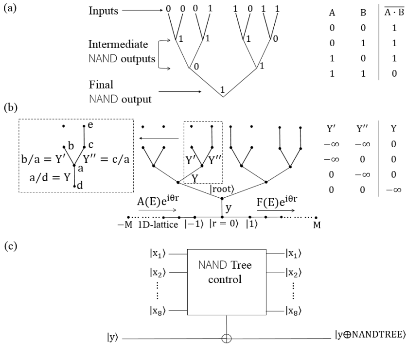
The classical NAND tree has inputs, intermediate NAND outputs and a final NAND output, as shown in Fig. 1(a). The inputs come in pairs and for the classical NAND tree, illustrated here, the inputs are given at the leaves. In general, the number of inputs is , where is the depth of the NAND tree (Fig. 1(a) has depth 3). The intermediate NAND outputs are given between the inputs and final NAND output, thus in the example of Fig. 1(a) the intermediate NAND outputs are (1,1), (1,0), and (0,1), and the final NAND output, the bit at the end of the computation, is (1). Farhi et al.’s[4] schematic representation of the quantum NAND tree is illustrated in Fig. 1(b), where each node corresponds to a site in the tight-binding (TB) Hamiltonian. As in the classical case, the inputs to the quantum NAND tree are given at the leaves and we control the inputs by connecting/disconnecting states. The intermediate NAND outputs are given between the inputs and the final NAND output, and the final NAND output is given at the bottom. The bits in the quantum truth table are , and setting and , renders the truth table for the quantum NAND gate equivalent to its classical counterpart. For the quantum NAND tree, we measure the final NAND output, , in the transmission coefficient. If the incoming particle is fully reflected the final NAND output is (0), or if the particle is fully transmitted the final NAND output is (1). Farhi et al. show that the run time to evaluate the quantum NAND tree, with a quantum algorithm, has a lower bound of with (number of leaves), where the run time for the best known classical algorithm is [4]. Thus, the quantum algorithm evaluates the final NAND output faster, which could enable investigation of systems, that are impossible, or limited, with classical algorithms. Fig. 1(c) shows the reversible circuit representation of the quantum NAND tree where the qubits work as inputs to the quantum NAND tree. The quantum NAND tree operates as a sequence of multi-control NOT gates where the bit flip acts on the output register.
2 Theory
For the quantum NAND tree, as suggested by Farhi et al.[4], we describe the system with a TB Hamiltonian with nearest-neighbor interactions. The single-particle Hamiltonian in the site representation, , of the atomic orbitals reads,
| (1) |
The first three terms sum over the states attached to the semi-infinite 1D-lattice with site energies and coupling elements given as and , respectively. The discrete basis states , where are the lattice states and we will take M to be very large. The last term, , is the TB Hamiltonian for the NAND tree and is defined similarly to the first three terms with only nearest-neighbour interactions included. For a semi-infinite 1D-lattice, the energy eigenstate and eigenvalue, , are given by and , respectively, with as the incoming momentum. For each , there is a scattering eigenstate of momentum , and from standard quantum scattering theory (QST), the scattering eigenstates are given by,
| (2) | ||||
| (3) |
where the NAND tree is located at and , , and are amplitudes of the incident, reflected, and transmitted particle, respectively, expressed in the -basis (site representation). The amplitude function of the transmitted particle is given by,
| (4) |
where the states and are illustrated in Fig. 1(b). We have assumed equal site energies and coupling elements, setting eV and eV (see supporting information S1). The quantity is an amplitude ratio of the scattering eigenstate between the states and and gives the final NAND output for the quantum NAND tree. All information regarding the tree i.e., the structure of the tree, coupling elements, site energies etc., are contained in . The transmission function is calculated from . Letting , depending on the leaf structure (inputs), the final NAND output, , takes the binary values,
| (5) |
For the final NAND output , the transmitted amplitude coefficient equals to zero, , and we measure the final NAND output (0) with a fully reflected particle. For the final NAND output , the transmitted amplitude coefficient equals the incident, , and we measure the final NAND output (1) with a fully transmitted particle. We evaluate the quantum NAND tree by starting from the inputs and moving down the tree, as in the classical NAND tree, and the bit values, , are the result of amplitude ratios between two connection states and by letting . For example, the input and NAND output for the leaf structure highlighted in Fig. 1(b) are given by (see supporting information S2),
| (6) |
Letting , the input becomes and , which results in the NAND output (). The other inputs, , , and , differ in leaf structure. While organic molecules are not normally included in systems proposed for quantum circuits, when the quantum random walk (the evolution of our system, Eq. (1), can be thought of as a quantum random walk) is recast as a scattering problem the formulation is reminiscent of systems previously studied in molecular electronics. When a conjugated organic molecule is modelled with a tight-binding Hamiltonian, each carbon atom can be represented by a single site and the nearest-neighbour interactions are determined by the nature of the carbon-carbon bonds. Imagining the tight-binding system as a molecule puts some restrictions on the topology and the assumptions outlined above need to be lifted to approach a chemically sensible system. In most cases, a molecule cannot be treated as having the same coupling elements and equal site energies across its entirely. Here, our goal is to realize the quantum NAND tree in a molecular system given realistic physical limitations of molecular platforms. Earlier work realizing Boolean truth tables with molecules using the Quantum Hamiltonian computation approach[10][11] has employed organic molecules and TB Hamiltonians for molecules on a surface[12][13][14][15].
3 Results and discussion
The first question as we move from the model to a molecule is whether we still have the value of a NAND gate function encoded in the transmission coefficient if we include variation in coupling elements and site energies throughout a quantum NAND tree. In Fig. 2, we show three different leaf structures, A, B, C, that are three different inputs to the quantum NAND gate and their corresponding NAND outputs. As previously mentioned, the input() is given as the amplitude ratio between two connection states, and , and the NAND output is given as the amplitude ratio . Cases 1-4 differ in their restrictions on coupling elements and site energies, and shaded green backgrounds indicate that bit values are preserved. The bit values are required in order to have a NAND gate function preserved in . In the simplest situation, case 1, coupling elements and site energies are kept constant with eV and eV, which is the assumption we have used up to this point. For , all inputs are bit values, hence the NAND gate function is preserved in . In case 2, we consider arbitrary negative coupling elements but site energies are kept constant. For , all inputs are bit values, hence the NAND gate function is preserved in and is independent of coupling strengths (see supporting information S2).
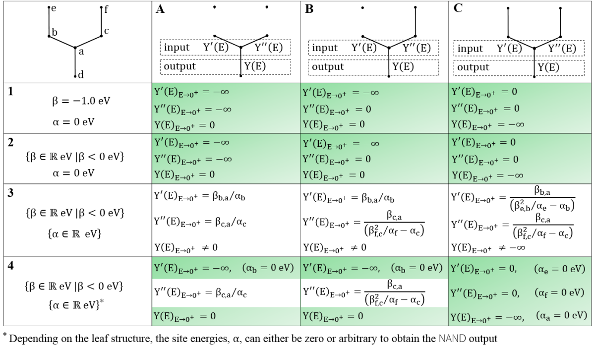
Next we evaluate the effect of variation in site energies. In case 3, we consider arbitrary negative coupling elements and arbitrary site energies, thus we have removed all restrictions. For , none of the bit values are preserved and the NAND gate function is not preserved in (see supporting information S3). In case 4, we tighten the restrictions again, considering arbitrary negative coupling elements but, depending on the leaf structure, the site energies are either restricted to zero or allowed to take an arbitrary value. For example, the leaf structure A should, in the ideal case, have input, which results in NAND output . However, this is only possible if all site energies, and , are zero. If we change only one of the site energies, for example eV, then the input still results in NAND output , since the input() is located in the denominator in the NAND output, . Hence, for the leaf structure A, we can change one of the two site energies, or , and still preserve the NAND output (). For the leaf structure B, the site energy is restricted to zero to preserve the NAND output (). For the leaf structure C that has the NAND output (), the three site energies , , and are all restricted to zero to preserve the NAND output (). From these analytical results, we can conclude that the NAND gate function can be maintained without restrictions on coupling elements, and site energies can be varied, depending on the input. With this relaxation of assumptions, we will build a model molecular system for the quantum NAND tree. We can map the TB model onto a conjugated molecular system, where we treat each site as a carbon or nitrogen atom in the -system and vary the coupling elements to model the single and double bonds in the molecule.
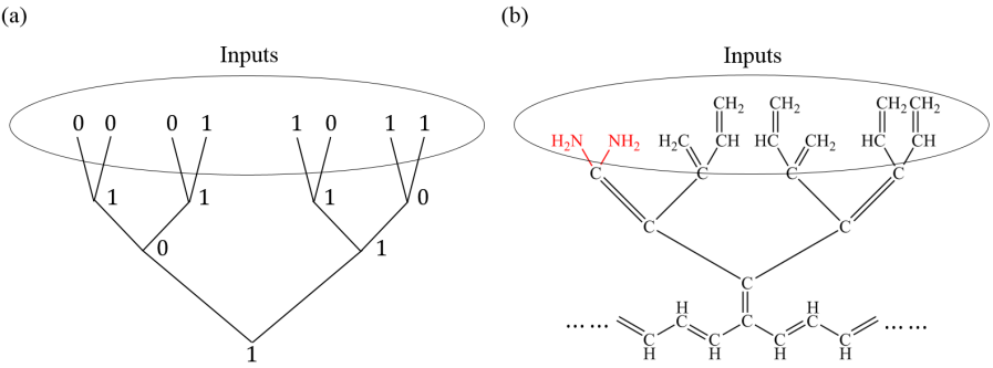
Fig. 3(b), a conjugated molecule, represents a quantum NAND tree, analogous to the classical NAND tree in Fig. 3(a) by having the same inputs. Here, the 1D-lattice is replaced with a carbon chain. We require the transmission coefficient at eV for the molecule in Fig. 3(b) to be close to one in order to measure the correct final NAND output (1). However, the structure of the NAND tree forces us to add two nitrogen atoms at the leaves in order to avoid unstable carbon radicals and, consequently, two site energies will differ from the rest of the NAND tree. As we saw in Fig. 2, changing two site energies for leaf structure A will affect the NAND output. We use the non-equilibrium Green’s function (NEGF) formalism to calculate the transmission with a 1D-lattice as the electrodes, following from prior work[16][17]. The transport calculations are performed using the TB model for the electronic structure, and we label the method as NEGF-TB. Fig. 4(a) and (b) show transmission as a function of the coupling element between nitrogen and carbon, , and the site energy for nitrogen, , at constant energy eV, and Fig. 4(c) shows transmission as a function of incoming energy [eV].
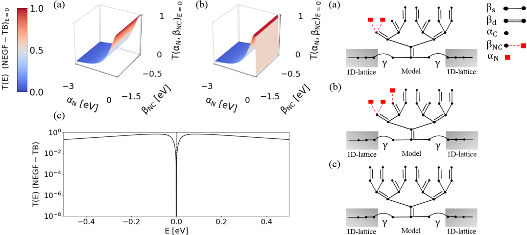
The NAND tree in Fig. 4(a) has the final NAND output (), which should translate to a high transmission at eV (see Eq. 5). When the site energy for nitrogen equals the site energy for carbon, eV, the particle is fully transmitted as expected from QST (Fig. 2), and we measure the final NAND output (). When the site energy for nitrogen differs from carbon (which is the case in reality), eV, the transmitted amplitude decreases, also expected from QST, because we are varying site energies that affect the transmission coefficient. As we approach eV, we see that . FIG. 4(b) differs in its input by having one more leaf bonded to a quantum state. The change in input, , results in the final NAND output () which we measure with a low transmission at eV. When the site energy for nitrogen equals the site energy for carbon, eV, the particle is fully reflected, , as expected from QST, otherwise for eV, the transmitted amplitude starts to increase. At eV, however, the transmission has decreased again to . The transmission ratio between the NAND trees (a) and (b) is 1, thus we cannot distinguish between the outputs (0) and (1) in this limit. Fig. 4(c) also has the final NAND output () but since the NAND tree consists of equal site energies only, destructive quantum interference (QI) is observed at eV, as expected from QST, given very low transmission as required. Here, the transmission ratio between the NAND trees (a) and (c) is large and one can easily distinguish between the outputs (0) and (1). Thus, for NAND trees where variation in site energies affect the final NAND output, as in Fig. 4(a) and (b), the magnitude of the site energy variation will determine whether we can distinguish the outputs (0) and (1). While this results from both a reduction in the high-transmission case and an increase in the low-transmission case, the dominant contribution comes from the many orders of magnitude increase in the low transmission. The reason is that the destructive QI effects at very rapidly looses its ability to suppress transmission with variation in site energies, as we saw in Fig. 4(b) with just by a few eV. Destructive QI effects in acyclic cross-conjugated systems, like the structures employed here, are sensitive to variation in site energies[19], thus, in this realisation, performance is significantly improved in NAND trees with equal site energies, as in Fig. 4(a) and (c). TB model calculations are, however, only a very approximate description of the molecular electronic structure. We can improve this description by using density function theory (DFT), allowing us to include both and electrons as well as a realistic non-planar geometry for the molecule. Fig. 5 shows the comparison between the NEGF-DFT and NEGF-TB for generation NAND molecules with linker groups to simulate the binding of these molecules to metal electrodes. The labels (0,0), (0,1), and (1,1) indicate the inputs, hence the red and blue molecules should have the final output (1) and the green molecule the final output (0), which is achieved with a high and a low transmission, respectively.
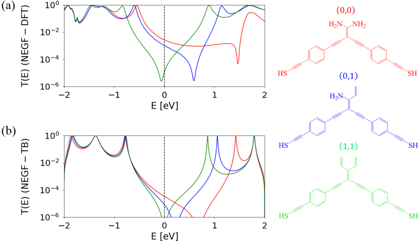
The molecule (1,1) consists of carbons only, thus all site energies are the same, eV, and destructive QI is observed at eV given very low transmission as required. In the NEGF-DFT transport calculations, the destructive QI features are also preserved during stretching and compression of the Au-S bond (see supporting information Figure S4). On the other hand, the inclusion of the nitrogen atoms clearly shifts the resonances away from the Fermi energy compared with all carbon systems, as expected from QST, so the high transmission required for the molecules (0,0) and (0,1) is not so successfully achieved. The NEGF-TB ratios are large, , see Table 3, thus the bit values are preserved within the TB model. The NEGF-DFT ratios, and , are 250 and 100 respectively, thus the bit values are preserved to some extent but reduced to a on/off transmission ratio.
| Molecule | A | B | ||||||
|---|---|---|---|---|---|---|---|---|
| (0,0) | 0 | 0 | 1 | 2.7 | 4.1 | |||
| (0,1) | 0 | 1 | 1 | 1.1 | 1.0 | |||
| (1,1) | 1 | 1 | 0 | 1.1 | 9.8 |
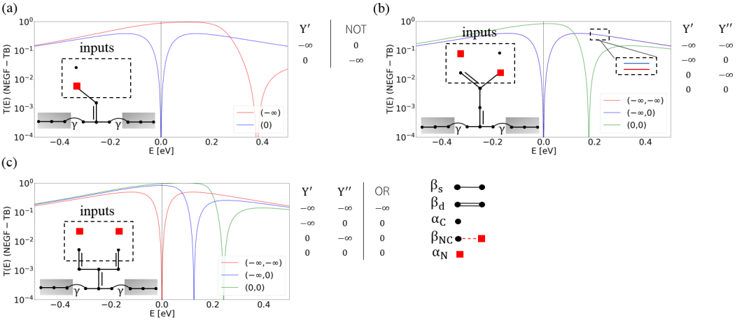
The same approach can be used to build other classical gates for quantum computing. Fig. 6 shows the classical gates, NOT, AND, and OR, their quantum structures, and NEGF-TB transport calculations to show their final outputs. The labels refer to the input for the logic gate, for example the label () for the NOT gate has input() and output() which we measure with a high transmission at . The inputs are given at the leaves and we control the inputs by connection/disconnection states, as we did in the quantum NAND tree.
4 Conclusion and Perspectives
In conclusion, by analyzing the quantum NAND tree, we showed the restrictions on the TB parameters required to maintain NAND gate function. An important result was the ability to vary coupling elements without affecting the NAND gate function, which indeed is a necessary condition when moving from the model to a molecule. The site energies could also be varied to some extent but there are significant restrictions on which site energies can vary while maintaining the NAND gate function. Further, we mapped the quantum NAND tree onto a conjugated molecule. Due to the structure of the NAND tree, we replaced some carbon atoms with nitrogen atoms, and, consequently, the destructive QI at Fermi-level very rapidly looses its ability to suppress transmission. Consequently, in some cases, the NAND outputs (0) and (1) were not successfully achieved. Beyond the issues associated with finding a suitable molecule, there are further physical processes that could well limit the function of a molecular NAND gate utilizing quantum interference. Namely: 1) Dephasing: Prior work studying charge transfer[21][22] and transport[23] has shown that destructive interference effects in molecules will indeed be suppressed (i.e. transmission increases) when dephasing is included in the calculations, this will effect the off state for the NAND gates. In all these cases, pure dephasing was introduced with a parameter, not from an ab initio calculation, and a realistic value for this parameter at a particular temperature is unknown. 2) Disorder/Geometric fluctuations: Even if we assume the electron transfer event is sufficiently fast (or instantaneous) such that pure dephasing is not a concern, we need to consider the effect of geometric fluctuations, both within the molecule and of the molecule in the junction. These kinds of fluctuations have been modeled by taking an ensemble of geometries from molecular dynamics simulations and calculating the transmission[23]. In that case, it was seen that these sorts of fluctuations will shift the peaks and dips in transmission in energy (effectively noise in the energy scale of the transmission plots) but sharp interference dips remain. 3) Inelastic transport: The final aspect to consider is whether transport processes beyond the elastic transport we have considered here could be significant, in particular, what is the magnitude of inelastic transport? Theoretical studies have shown that while there may certainly be significant inelastic contributions to the current, the pronounced suppression as a result of destructive interference is not completely removed[24][25]. All the studies listed above were theoretical, and none considered all aspects at once. Consequently, the question still remains as to whether the sum total of these processes might present a problem, even if each one alone does not. At this stage this has not been quantified, but the extremely small size of the molecular components and the fact that significant interference effects have been observed experimentally at room temperature[26][27], suggests that destructive interference effects persist despite these physical processes. The choice of an acyclic cross-conjugated system for the molecular realization of the quantum NAND tree yields a molecule with a Hückel Hamiltonian that was as similar as possible to the tight binding model from the original work. The problem however, is that not all of the tight-binding systems correspond to stable molecular systems without modification. The general principle of the quantum NAND tree, that QI interference effects can be switched on and off with substituents and thereby give NAND function, can of course be explored with many other systems known to result in destructive QI. Many systems have been explored for this purpose, for example, meta-substituted benzene rings, five-membered rings, and quinoidal structures[28][29]. It remains an open question as to whether any of these systems would offer improved performance as a NAND gate, in particular offering a larger transmission ratio for the final NAND outputs. Another challenge that remains is how best to change the logical inputs for the quantum NAND tree. Here, this was achieved by connection/disconnection of substituents, which is not suitable for experiments. Soe et al.[14] have conducted scanning tunneling microscopy (STM) experiments realizing Boolean truth tables through molecules, including changing the logical inputs. In that case, their synthesized molecule is physisorbed on a Au(111) surface (the -system is preserved), and current tunnels from the STM tip, through the molecule, to the surface. As in the quantum NAND tree, the logic gate function is encoded in the transmission, and they control the inputs by contacting or detaching Au atoms at the top of the molecule. While a practical realization of the quantum NAND tree in a molecular system remains elusive, it is clear that there is a viable strategy for future investigation. The molecular nature of quantum interference effects in molecules, with their observation in many molecular systems at room temperature, suggest that molecules should be ideal for this purpose if the right molecular structures can be found. Chemical space is certainty vast but until recently chemists have not focused on developing chemical insight for these sort of applications. As research into quantum interference effects in molecules progresses, so too may we see the emergence of molecular candidates for quantum realization of classical logic gates, or even quantum gates.
Acknowledgements
We thank Magnus F. Bøe, Anders Jensen, Marc H. Garner, Idunn Prestholm, Thorsten Hansen and Christian Joachim for helpful discussions. This research was supported by the Danish Chemical Society, Oticon Fund, Julie Damms Fund, Copenhagen Education Fund, Knud Højgaards Fund, Henry and Mary Skovs Fund, Viet - Jacobsens Fund, Villum Foundation, Carlsberg Foundation, the Danish Council for Independent Research Natural Sciences, and the Vannevar Bush Faculty Fellowship program sponsored by the Basic Research Office of the Assistant Secretary of Defense for Research and Engineering and funded by the Office of Naval Research through grant N00014-16-1-2008.
References
References
- [1] D. Deutsch and R. Jozsa, “Rapid Solution of Problems by Quantum Computation,” Proceedings of the Royal Society A: Mathematical, Physical and Engineering Sciences, vol. 439, pp. 553–558, dec 1992.
- [2] P. W. Shor, “Polynomial-Time Algorithms for Prime Factorization and Discrete Logarithms on a Quantum Computer,” SIAM Journal on Computing, vol. 26, pp. 1484–1509, oct 1997.
- [3] E. Farhi and S. Gutmann, “Quantum computation and decision trees,” Physical Review A, vol. 58, pp. 915–928, aug 1998.
- [4] E. Farhi, J. Goldstone, and S. Gutmann, “A Quantum Algorithm for the Hamiltonian NAND Tree,” Theory of Computing, vol. 4, no. 1, pp. 169–190, 2008.
- [5] A. M. Childs, “Universal Computation by Quantum Walk,” Physical Review Letters, vol. 102, p. 180501, may 2009.
- [6] A. M. Childs, D. Gosset, and Z. Webb, “Universal Computation by Multiparticle Quantum Walk,” Science, vol. 339, pp. 791–794, feb 2013.
- [7] A. M. Childs and D. J. Strouse, “Levinson’s theorem for graphs,” Journal of Mathematical Physics, vol. 52, p. 082102, aug 2011.
- [8] A. M. Childs and D. Gosset, “Levinson’s theorem for graphs II,” Journal of Mathematical Physics, vol. 53, p. 102207, oct 2012.
- [9] J. D. Whitfield, C. A. Rodríguez-Rosario, and A. Aspuru-Guzik, “Quantum stochastic walks: A generalization of classical random walks and quantum walks,” Physical Review A, vol. 81, p. 022323, feb 2010.
- [10] G. Dridi, R. Julien, M. Hliwa, and C. Joachim, “The mathematics of a quantum Hamiltonian computing half adder Boolean logic gate,” Nanotechnology, vol. 26, p. 344003, aug 2015.
- [11] G. Dridi, O. F. Namarvar, and C. Joachim, “Qubits and quantum Hamiltonian computing performances for operating a digital Boolean 1/2-adder,” Quantum Science and Technology, vol. 3, p. 025005, apr 2018.
- [12] A. Kleshchonok, R. Gutierrez, C. Joachim, and G. Cuniberti, “Quantum interference based Boolean gates in dangling bond loops on Si(100):H surfaces,” Scientific Reports, vol. 5, p. 14136, nov 2015.
- [13] C. Joachim, N. Renaud, and M. Hliwa, “The Different Designs of Molecule Logic Gates,” Advanced Materials, vol. 24, pp. 312–317, jan 2012.
- [14] W.-H. Soe, C. Manzano, N. Renaud, P. de Mendoza, A. De Sarkar, F. Ample, M. Hliwa, A. M. Echavarren, N. Chandrasekhar, and C. Joachim, “Manipulating Molecular Quantum States with Classical Metal Atom Inputs: Demonstration of a Single Molecule NOR Logic Gate,” ACS Nano, vol. 5, pp. 1436–1440, feb 2011.
- [15] C. Joachim, I. Duchemin, J. F. Sek, and N. J. Cerf, “HAMILTONIAN LOGIC GATES: COMPUTING INSIDE A MOLECULE,” International Journal of Nanoscience, vol. 4, no. 1, pp. 107–118, 2005.
- [16] M. G. Reuter, T. Hansen, T. Seideman, and M. A. Ratner, “Molecular Transport Junctions with Semiconductor Electrodes: Analytical Forms for One-Dimensional Self-Energies †,” The Journal of Physical Chemistry A, vol. 113, pp. 4665–4676, apr 2009.
- [17] D. Brisker, I. Cherkes, C. Gnodtke, D. Jarukanont, S. Klaiman, W. Koch, S. Weissman, R. Volkovich, M. C. Toroker, and U. Peskin, “Controlled electronic transport through branched molecular conductors,” Molecular Physics, vol. 106, pp. 281–287, feb 2008.
- [18] W. P. Purcell and J. A. Singer, “A brief review and table of semiempirical parameters used in the Hueckel molecular orbital method,” Journal of Chemical & Engineering Data, vol. 12, pp. 235–246, apr 1967.
- [19] G. C. Solomon, D. Q. Andrews, R. H. Goldsmith, T. Hansen, M. R. Wasielewski, R. P. Van Duyne, and M. A. Ratner, “Quantum Interference in Acyclic Systems: Conductance of Cross-Conjugated Molecules,” Journal of the American Chemical Society, vol. 130, pp. 17301–17308, dec 2008.
- [20] J. P. Perdew, K. Burke, and M. Ernzerhof, “Generalized Gradient Approximation Made Simple,” Physical Review Letters, vol. 77, pp. 3865–3868, oct 1996.
- [21] R. H. Goldsmith, M. R. Wasielewski, and M. A. Ratner, “Electron Transfer in Multiply Bridged Donor−Acceptor Molecules: Dephasing and Quantum Coherence,” The Journal of Physical Chemistry B, vol. 110, pp. 20258–20262, oct 2006.
- [22] R. H. Goldsmith, M. R. Wasielewski, and M. A. Ratner, “Scaling Laws for Charge Transfer in Multiply Bridged Donor/Acceptor Molecules in a Dissipative Environment,” Journal of the American Chemical Society, vol. 129, pp. 13066–13071, oct 2007.
- [23] D. Q. Andrews, G. C. Solomon, R. H. Goldsmith, T. Hansen, M. R. Wasielewski, R. P. V. Duyne, and M. A. Ratner, “Quantum Interference: The Structural Dependence of Electron Transmission through Model Systems and Cross-Conjugated Molecules,” The Journal of Physical Chemistry C, vol. 112, pp. 16991–16998, oct 2008.
- [24] T. Markussen and K. S. Thygesen, “Temperature effects on quantum interference in molecular junctions,” Physical Review B, vol. 89, p. 085420, feb 2014.
- [25] J. Lykkebo, A. Gagliardi, A. Pecchia, and G. C. Solomon, “IETS and quantum interference: Propensity rules in the presence of an interference feature,” The Journal of Chemical Physics, vol. 141, p. 124119, sep 2014.
- [26] M. H. Garner, H. Li, Y. Chen, t. A. Su, Z. Shangguan, D. W. Paley, T. Liu, F. Ng, H. Li, S. Xiao, C. Nuckolls, L. Venkataraman, and G. C. Solomon, “Comprehensive suppression of single-molecule conductance using destructive -interference,” Nature, vol. 558, pp. 415–419, jun 2018.
- [27] C. M. Guédon, H. Valkenier, T. Markussen, K. S. Thygesen, J. C. Hummelen, and S. J. van der Molen, “Observation of quantum interference in molecular charge transport,” Nature Nanotechnology, vol. 7, pp. 305–309, may 2012.
- [28] M. H. Garner, G. C. Solomon, and M. Strange, “Tuning Conductance in Aromatic Molecules: Constructive and Counteractive Substituent Effects,” The Journal of Physical Chemistry C, vol. 120, pp. 9097–9103, may 2016.
- [29] A. Borges and G. C. Solomon, “Effects of Aromaticity and Connectivity on the Conductance of Five-Membered Rings,” The Journal of Physical Chemistry C, vol. 121, pp. 8272–8279, apr 2017.