[cor1]Corresponding author: schwier@hiroshima-u.ac.jp
aff1]Hiroshima Synchrotron Radiation Center, Hiroshima University, 2-313 Kagamiyama, Higashi-Hiroshima 739-0046, Japan
aff2]Graduate School of Science, Hiroshima University, 1-3-1 Kagamiyama, Higashi-Hiroshima 739-8526, Japan
aff3]Diamond Light Source, Harwell Campus, Didcot OX11 0DE, United Kingdom
aff4]DESY Photon Science, Deutsches Elektronen-Synchrotron, D-22603 Hamburg, Germany
aff5]Clarendon Laboratory, Department of Physics, University of Oxford, Parks Road, Oxford OX1 3PU, United Kingdom
aff6]Institute for Solid State Physics, Karlsruhe Institute of Technology, 76021 Karlsruhe, Germany
Applications for ultimate spatial resolution in LASER based -ARPES: A FeSe case study
Abstract
Combining Angle resolved photoelectron spectroscopy (ARPES) and a -focused Laser, we have performed scanning ARPES microscopy measurements of the domain population within the nematic phase of FeSe single crystals. We are able to demonstrate a variation of the domain population density on a scale of a few 10 m while constraining the upper limit of the single domain size to less than 5 . This experiment serves as a demonstration of how combining the advantages of high resolution Laser ARPES and an ultimate control over the spatial dimension can improve investigations of materials by reducing the cross contamination of spectral features of different domains.
1 Introduction
In this paper we present data from the material FeSe, which demonstrate the full potential of laser based -ARPES to probe with both high energy resolution, giving precision on the anisotropic electronic state, and high spatial resolution, giving information on the distribution of orthorhombic domains in the nematic state. Interest in the material arises due to its two separate phase transitions; at 90 K marks an unusual tetragonal-orthorhombic distortion, entering the so-called nematic phase characterized by in-plane electronic anisotropy, and at K the system displays unconventional superconductivity [1]. In other Fe-based superconductors, a similar structural transition, , precedes the onset of magnetic ordering in certain systems [2], but FeSe is unique in that it does not show antiferromagnetic order at any temperature. The interest in this phase transition has been fueled by the intriguing observations of strong electronic effects occurring around , with the observation of a divergent “nematic susceptibility” in samples under tensile strain [3, 4], as well as the pronounced influence of nematic order on the two-fold symmetric superconducting gap structure [5].
High quality single crystals of FeSe grow in the tetragonal space group P4/nmm. Typical samples have dimensions of mm3. The crystallographic phase transition to an orthorhombic low temperature phase at K [6] is subtle but sharp. The reduced symmetry of the low temperature phase makes the and axes inequivalent. Unless controlled by uniaxial strain, the sample will naturally form regions with the axis aligned along either of two orthogonal directions with equal probability, analogous to domain formation in ferromagnets cooled in zero field. These regions have been found to form domains by optical microscopy techniques such as optical polarized light imaging [4] and photo-induced reflectivity [7], as well as scanning tunneling microscopy [8, 5]. A relation to the anisotropy of the electronic structure was first established in Rb-intercalated samples by combined structural and electronic structure microscopy studies [9, 10]. The interplay between structural distortion and electronic structure was found to be crucial for understanding the enhanced superconductivity up to K. In all samples of FeSe as well as Rb-intercalated FeSe domains of varying size and shape have been found.
Photoemission spectroscopy, and in particular the momentum-resolved ARPES has been the chosen technique in many studies of FeSe through the tetragonal-to-orthorhombic phase transition at [11, 12, 13, 14, 15, 16]. However, the large size of the beam spot of conventional ARPES systems leads to the simultaneous observation of two copies of the momentum-resolved structures, thus complicating the analysis. It was thus attempted early on to force the samples into only one crystallographic orientation by application of slight uniaxial stress during cooling (de-twinning). ARPES data from such samples have given an unambiguous view of all electronic bands and their momentum structure and Fermi surface [17, 18, 19]. Residual intensity from domains of suppressed orientation is, however, persistently visible in such measurements [18, 20], and the external strain on the samples can cause experimental issues, such as surface bending and cracking. This motivates a second approach, which we take here, to shrink the size of the beam to become comparable with the domain size. In the ideal case one could directly measure photoelectrons from one domain only, but in a more realistic scenario corresponding to current capabilities, local strains in the sample can give regions dominated by a particular domain orientation, giving strong contrast in the ARPES dispersions measured at different locations.
2 Result and Discussion
The experiments were performed at the -LaserARPES machine at the Hiroshima Synchrotron Radiation Center (HiSOR). A detailed performance evaluation of the system has been described in [21]. For the experiment a photon energy of eV was used. If not stated otherwise the photons were linearly polarized with an angle of 60∘ against p-polarized light. The angle was chosen by comparing the relative intensity of the four hole pocket bands crossing the Fermi level around the -point and subsequently optimizing the polarization to maximize the visibility of all four bands.
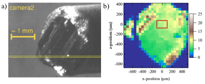
FeSe samples were grown by vapor transport [13] and stored under Ar atmosphere before the measurement. Samples were cleaved in-situ via the top-post method at a temperature of T = 20 K. During the measurement the temperature was kept at 20 K via a resistive heater mounted behind the sample holder inside the manipulator stage [22]. Following the cleave, the homogeneity of the sample surface was first verified via an optical long-distance microscope mounted to the measurement chamber (Fig. 1 a). While the surface appears not perfectly flat, past experience with FeSe tells that such a surface can be considered a good cleave. From a LaserARPES point of view, care has to be given to the absence of flakes and edge deformation in order to reduce the risk of encountering unwanted distortion and artefacts in the spectrum, a rather common occurrence in low-energy ARPES measurements.

After obtaining an optically sufficient cleave, the homogeneity of the surface was further verified by obtaining a rough spatial map of the electronic structure (henceforth “topography”) across the sample. For this an ARPES measurement of the electronic band structure at the Fermi level around the -point was performed for each point within a 1.3 1.3 mm area using a step size of 50 . By integrating the total intensity within the detector range Fig. 1 b) was obtained. Since the data acquisition allows for the manual analysis of the ARPES spectrum at each point the choice of a suitable measurement area is based on homogeneity as well as the experimenters judgement of the ARPES features.
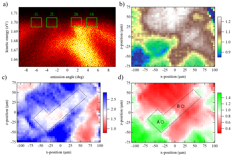
After choosing a suitable area (marked as the red rectangle in Fig 1 b)) a second spatial ARPES map was obtained. An area of 150 210 was chosen and rastered with a step size of 5 . A representative example of a single raw ARPES spectrum is shown in Fig. 2 a). Green rectangles indicate the regions of interest (ROI) set up to analyze the spectral weight from the inner and outer hole pocket bands. Each are expected to be related to a twinned orthorhombic domain in the nematic phase of FeSe. Before moving to a detailed analysis of the obtained data, the topography is again plotted as a reference of the surface homogeneity in Fig. 2 b). Note that while clear structures are identifiable in the topography, the ARPES quality is of comparable quality across the measurement area. Furthermore, variation of the total intensity has to be considered a sum effect of the real topography variations as well as matrix elements effects and sample orientation.

The goal of this study is to resolve the variation in population of the two twinned orthorhombic domains, a task for which the topography is not a suitable indicator. However, stored within the spatial ARPES map are the spectral weight of the electronic structure at each point in the mapping. Therefore, by a careful choice of ROIs corresponding to distinct features in the ARPES spectra, one could process the data in a way to obtain domain contrast. Care has to be given to the fact that large amounts of data are automatically processed. In such a case it is useful to define a quality parameter first.
Not only in the current case, but more generally, the sample orientation can be used as a guide to detect the unwanted influence of intrinsic (sample topography, surface bending) and extrinsic effects (local electric fields, sample edge effects). If we consider the electronic structure in each of the orthorhombic domains in FeSe we find that the outer hole pocked (represented by ROIs: 1L & 1R) and the inner hole pocket (represented by ROIs: 2L & 2R) have vastly different dispersion parallel and perpendicular to the analyzer detection plane. This fact leads to the choice of 1L/1R as a figure of merit representing a constant orientation of the sample within our measurement range. In Fig. 2 c) we have plotted this ratio. White color represents an orientation corresponding to emission from a cut along (as judged by manual review of the ARPES spectra), while red and blue represent areas with deviations of the . Based on this map, we choose to focus on the area with constant orientation (dashed rectangle) for further analysis of the domain population. While other parts of the sample will also exhibit different domain population, the loss of well-defined orientation makes these areas unsuited for analysis under the current geometry (manipulator polar and tilt angles).
Coming back to the original idea of attributing the two hole pockets as representing a superposition of photoemission from the two twinned domains, it is now required to chose how best to represent the contrast between an overpopulation of each of the two domains. In the present case, the ratio of 1R/2L preduces the highest contrast as 1R and 2L exhibit the highest intensity variation across the selected area of interest. Plotting this ratio in Fig. 2 d) allowed us to identify regions on the surface with domain overpopulation. It should be noted though that it is not possible to discuss absolute domain population and therefore an intensity ratio of unity in Fig. 2 d) does not necessarily correspond to a domain population ratio of 1:1. Since the hole pockets are expected to originate from different orbitals, it would be rather surprising if such a correspondence could be found. Here the color scale was chosen in such a way that within the rectangle of constant orientation, the lowest and highest values would be represented as the brightest green and red respectively.
Based on the presence of spectral weight from both hole pockets in all spectra of our map, the size of a single orthorhombic domain is estimated to be well below the photon spot size of 5 . To still be able to highlight the variation in domain population we now choose two points (A and B) each representing a maximum and minimum of the 1R/2L ratio for further detailed measurements.
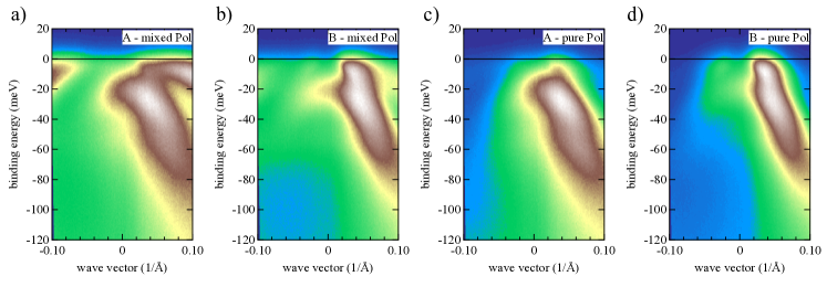
In Fig. 3 a) and b) we have plotted high resolution spectra obtained from points A and B on the sample. It should be noted that in both measurement points all four bands are crossing the Fermi level, albeit with strongly differing intensities. While at A, the outer hole pocket is dominating, at B we find the reverse situation. Since the of the bands in both spectra are the same, the intensity variation can only be explained by a variation of the domain population with the area of sample being probed by the spot at the two locations. Such a variation is in accordance with the assumption that twinned domains coexist on the single crystalline surface within the nematic phase.

To illustrate that not only a high spatial resolution, but also the choice of light polarization plays a significant role in resolving the spatial variation of the spectral weight, we have plotted spectra obtained with pure linear polarization in Fig. 3 c) and d). Here the polarization was tuned to correspond to p-polarization [21] and both points, A and B were measured again. While differences are still present between both spectra, they are obviously less pronounced and moreover emission from the outer hole pocket is strongly suppressed, making it much more difficult to determine population differences employing pure linear polarization.

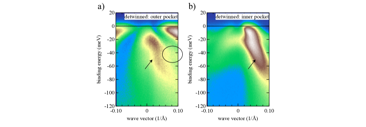
Under the assumption that the spectra at both A and B are a linear superposition of emission from the two twinned domains within the area illuminated by the laser spot, it should be possible to separate the emission from each domain by adjusting the relative weight ( and ) of each spectra in Fig. 3 a) and b). The emission from the domains with the outer and inner hole pockets ( and ) can then be obtained by adjusting the normalization factors in such a way that the minimum intensity in the resulting spectra does not become negative, i.e. unphysical. The resulting spectra are shown in Fig. 4 a) and b). At the Fermi level, the spectral weight in each plot is entirely dominated by the outer and inner hole pocket respectively, removing any visible cross-contamination from the other domain. At higher binding energies the spectral weight is less separated; the nematic effects are most pronounced near , where also the features are sharpest. The occupied and lighter inner hole pocket (arrows) is present in both spectra, though with unequal distribution of spectral weight, related via the matrix element effects to the different orbital character on the two cut directions. An additional heavier hole-like dispersion is detected in Fig. 4 a (circle).
Comparing these numerical detwinning results with strain mediated detwinning [19] as well as effective detwinning making use of light polarization [23] is however going beyond the scope of this paper, since the spectral weight is highly dependent on the photoemission geometry and used excitation energies.
In conclusion, this work marks an important step towards demonstrating the capabilities of laser-based -ARPES. Choosing the well-studied FeSe system allows for direct comparison of the advantages of surface selectivity in our system compared to common Laser ARPES measurements with spot sizes of the order of several 10 and above as well as modern high resolution ARPES synchrotron endstations with similar photon spot size limitations. At the same time, this study could resolve spatial inhomogeneity in the domain population of FeSe in unstrained samples on the scale opening up pathways to probe local strain effects without the necessity to apply external strain. A follow-up study should focus on the aspects of temperature dependence of the spatial inhomogeneity as well as the shape and polarization dependence of the Fermi surface with and without numerical detwinning. In the absence of a deflection or image type analyzer, particularly the latter task, while not impossible, poses a significant challenge to a -ARPES machine and puts a high demand on the sample surface quality due to distortion of the local electric field.
3 Acknowledgments
The authors would like to thank the Hiroshima N-Bard for supplying liquid Helium. We also wish to thank H. Namatame and M. Taniguchi for discussions and leadership that led to the creation of the -Laser ARPES machine. The high precision of the spatial measurements are thanks to the “nano-stage” developed by Y. Aiura and its software control developed by H. Iwasawa. Beamtime at the HSRC was granted under proposal number 16BU008. A.A.H. acknowledges the financial support of the Oxford Quantum Materials Platform Grant (EP/M020517/1).
References
- Böhmer and Kreisel [2018] A. E. Böhmer and A. Kreisel, Journal of Physics: Condensed Matter 30, p. 023001 (2018).
- Fernandes, Chubukov, and Schmalian [2014] R. M. Fernandes, A. V. Chubukov, and J. Schmalian, Nature Physics 10, 97 EP –01 (2014).
- Böhmer et al. [2015] A. E. Böhmer, T. Arai, F. Hardy, T. Hattori, T. Iye, T. Wolf, H. v. Löhneysen, K. Ishida, and C. Meingast, Phys. Rev. Lett. 114, p. 027001Jan (2015).
- Tanatar et al. [2016] M. A. Tanatar, A. E. Böhmer, E. I. Timmons, M. Schütt, G. Drachuck, V. Taufour, K. Kothapalli, A. Kreyssig, S. L. Bud’ko, P. C. Canfield, R. M. Fernandes, and R. Prozorov, Phys. Rev. Lett. 117, p. 127001Sep (2016).
- Sprau et al. [2017] P. O. Sprau, A. Kostin, A. Kreisel, A. E. Böhmer, V. Taufour, P. C. Canfield, S. Mukherjee, P. J. Hirschfeld, B. M. Andersen, and J. C. S. Davis, Science 357, 75–80 (2017), http://science.sciencemag.org/content/357/6346/75.full.pdf .
- McQueen et al. [2009] T. M. McQueen, A. J. Williams, P. W. Stephens, J. Tao, Y. Zhu, V. Ksenofontov, F. Casper, C. Felser, and R. J. Cava, Phys. Rev. Lett. 103, p. 057002Jul (2009).
- Luo et al. [2017] C.-W. Luo, P. Chung Cheng, S.-H. Wang, J.-C. Chiang, J.-Y. Lin, K.-H. Wu, J.-Y. Juang, D. A. Chareev, O. S. Volkova, and A. N. Vasiliev, npj Quantum Materials 2, p. 32 (2017).
- Kasahara et al. [2014] S. Kasahara, T. Watashige, T. Hanaguri, Y. Kohsaka, T. Yamashita, Y. Shimoyama, Y. Mizukami, R. Endo, H. Ikeda, K. Aoyama, T. Terashima, S. Uji, T. Wolf, H. von Löhneysen, T. Shibauchi, and Y. Matsuda, Proceedings of the National Academy of Sciences 111, 16309–16313 (2014), http://www.pnas.org/content/111/46/16309.full.pdf .
- Speller et al. [2014] S. C. Speller, P. Dudin, S. Fitzgerald, G. M. Hughes, K. Kruska, T. B. Britton, A. Krzton-Maziopa, E. Pomjakushina, K. Conder, A. Barinov, and C. R. M. Grovenor, Phys. Rev. B 90, p. 024520Jul (2014).
- Speller, Mousavi, and Dudin [2015] S. Speller, T. Mousavi, and P. Dudin, Novel Superconducting Materials 1, p. 29 (2015).
- Maletz et al. [2014] J. Maletz, V. B. Zabolotnyy, D. V. Evtushinsky, S. Thirupathaiah, A. U. B. Wolter, L. Harnagea, A. N. Yaresko, A. N. Vasiliev, D. A. Chareev, A. E. Böhmer, F. Hardy, T. Wolf, C. Meingast, E. D. L. Rienks, B. Büchner, and S. V. Borisenko, Phys. Rev. B 89, p. 220506Jun (2014).
- Nakayama et al. [2014] K. Nakayama, Y. Miyata, G. N. Phan, T. Sato, Y. Tanabe, T. Urata, K. Tanigaki, and T. Takahashi, Phys. Rev. Lett. 113, p. 237001Dec (2014).
- Watson et al. [2015] M. D. Watson, T. K. Kim, A. A. Haghighirad, N. R. Davies, A. McCollam, A. Narayanan, S. F. Blake, Y. L. Chen, S. Ghannadzadeh, A. J. Schofield, M. Hoesch, C. Meingast, T. Wolf, and A. I. Coldea, Phys. Rev. B 91, p. 155106Apr (2015).
- Zhang et al. [2015] P. Zhang, T. Qian, P. Richard, X. P. Wang, H. Miao, B. Q. Lv, B. B. Fu, T. Wolf, C. Meingast, X. X. Wu, Z. Q. Wang, J. P. Hu, and H. Ding, Phys. Rev. B 91, p. 214503Jun (2015).
- Fanfarillo et al. [2016] L. Fanfarillo, J. Mansart, P. Toulemonde, H. Cercellier, P. Le Fèvre, F. m. c. Bertran, B. Valenzuela, L. Benfatto, and V. Brouet, Phys. Rev. B 94, p. 155138Oct (2016).
- Watson et al. [2016] M. D. Watson, T. K. Kim, L. C. Rhodes, M. Eschrig, M. Hoesch, A. A. Haghighirad, and A. I. Coldea, Phys. Rev. B 94, p. 201107Nov (2016).
- Yi et al. [2011] M. Yi, D. Lu, J.-H. Chu, J. G. Analytis, A. P. Sorini, A. F. Kemper, B. Moritz, S.-K. Mo, R. G. Moore, M. Hashimoto, W.-S. Lee, Z. Hussain, T. P. Devereaux, I. R. Fisher, and Z.-X. Shen, Proceedings of the National Academy of Sciences 108, 6878–6883 (2011), http://www.pnas.org/content/108/17/6878.full.pdf .
- Shimojima et al. [2014] T. Shimojima, Y. Suzuki, T. Sonobe, A. Nakamura, M. Sakano, J. Omachi, K. Yoshioka, M. Kuwata-Gonokami, K. Ono, H. Kumigashira, A. E. Böhmer, F. Hardy, T. Wolf, C. Meingast, H. v. Löhneysen, H. Ikeda, and K. Ishizaka, Phys. Rev. B 90, p. 121111Sep (2014).
- Watson et al. [2017a] M. D. Watson, A. A. Haghighirad, L. C. Rhodes, M. Hoesch, and T. K. Kim, New Journal of Physics 19, p. 103021 (2017a).
- Watson et al. [2017b] M. D. Watson, A. A. Haghighirad, H. Takita, W. Mansuer, H. Iwasawa, E. F. Schwier, A. Ino, and M. Hoesch, Journal of the Physical Society of Japan 86, p. 053703 (2017b), https://doi.org/10.7566/JPSJ.86.053703 .
- Iwasawa et al. [2017] H. Iwasawa, E. F. Schwier, M. Arita, A. Ino, H. Namatame, M. Taniguchi, Y. Aiura, and K. Shimada, Ultramicroscopy 1–7june (2017).
- [22] The use of the heater has been verified to not influence the ARPES measurement. No influence of a heating current induced magnetic field was found in the ARPES spectrum, .
- Rhodes et al. [2018] L. C. Rhodes, M. D. Watson, A. A. Haghighirad, D. V. Evtushinsky, M. Eschrig, and T. K. Kim, arXiv p. 1804.01436 (2018).
- [24] Here we choose to set the color scale in such a way that within the chosen area of interest of constant orientation, the lowest and highest values would be represented as the brightest green and red respectively, .
- Hosono et al. [2018] H. Hosono, A. Yamamoto, H. Hiramatsu, and Y. Ma, Materials Today 21, 278 – 302 (2018).