Near-Perfect Absorption of Light by Plasmene Sheets
Abstract
Near-perfect absorbers (NPAs) efficiently absorb visible light with a layered nanostructure that is thinner than the diffusion lengths of photogenerated charge carriers. We overcame existing limitations in fabricating their nanoparticulate surface by depositing plasmene, a tightly-packed two-dimensional lattice of metal nanoparticles formed through self-assembly. The plasmene NPAs absorb up to 98% of incident visible light, with modelling showing the improvement on existing NPAs arises from the structural ordering of the plasmene. We also demonstrate control of NPAs’ absorption profile through the use of anisotropic building blocks in plasmene. These property enhancements may broaden the application of NPAs to structural colour, sensing and photocatalysis.
keywords:
Plasmonics, metasurfaces, optical magnetic mode, perfect absorption1 Introduction
Solar energy harvesting in photovoltaics and photocatalysis begins with the absorption of light by matter 1. Light absorption creates electronically excited states from which useful work can be extracted if the excited charge carriers can readily access chemical (catalytic site) or physical (electrode) interfaces. To maximize solar-energy conversion efficiencies, it is thus desirable to create light-harvesting devices in which the thickness of the absorbing layer is much smaller than characteristic charge-carrier scattering lengths, whilst simultaneously preserving a high magnitude of light absorption 2.
One class of structure that embodies these properties is the near-perfect absorber (NPA), in which near-complete light absorption occurs on a sub-wavelength scale due to optical impedance matching between the material and free space. Optical impedance matching can be achieved by placing a layer of nanoscale resonators at a specific distance from a reflector, leading to the excitation of optical resonances that efficiently suppress the reflection of light. The presence of the mirror eliminates transmission, and consequently nearly all light is absorbed. This concept has been demonstrated using metallic (plasmonic) nanostructures, resulting in strong absorption bands in the infrared 3, 4, 5, 6 and visible 7, 8 range of the electromagnetic spectrum. Notably, there are remarkable examples where broadband light absorption has been achieved 9, 10, 11, 12, 5.
In most demonstrations of plasmonic NPAs, the metallic nanostructures have been lithographically defined into periodic arrays or consist of randomly distributed nanoparticles, which result from the vacuum deposition and subsequent annealing of thin metal layers. In contrast, creating these structures using colloidal suspensions of high quality nanoparticles would enable the facile fabrication of NPAs using simple and scalable deposition processes. A theoretical study suggested that for a planar periodic array of lossy small particles (such as metal colloids) to exhibit perfect absorption, the absorption cross-section of an individual member of said array must be comparable to the area of the unit cell. 13 This implies that the use of metal colloids as the building blocks of NPAs requires their assembly into surfaces of moderate to high particle densities. To date, colloid-based plasmonic NPA structures have been realized by the deposition of nanocubes using a self-assembly approach driven by the electrostatic attraction of colloids to the supporting substrates. However, this leads to relatively low surface coverages ( 4.2% coverage 14) and parasitic light scattering from the formed surfaces 14, 15, 8.
Plasmene is a highly ordered and tightly-packed two-dimensional sheet of metal nanoparticles formed by spontaneous self-assembly at an air-water interface 16, 17, 18, 19, 20. These sheets are of single-particle thickness and form over macroscopic (i.e. 3 mm) lateral dimensions. They also demonstrate several unique fundamental properties, such as an unusually high mechanical strength ( 1GPa Young’s modulus) and the capacity to support both propagating and gap plasmon modes, controllable by tuning the geometry of plasmene’s unit cell 18.
Here, we demonstrate near-perfect absorbers made with a nanostructured absorber layer of plasmene. The high surface coverage provided by plasmene creates NPAs that absorb up to 98% of incident visible light. Furthermore, engineering the geometry of the plasmene building blocks allows for control of the wavelength of absorption.
2 Results and Discussion
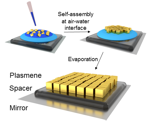
The basic architecture of the plasmene NPAs, shown in Figure 1, consists of three distinct layers: a mirror, a thin dielectric spacer, and a single layer of plasmene. Plasmene sheets with building blocks of Au nanocubes (shown in Figure 2B) were synthesized following well-established protocols (Figure 2A) 21, 20. Suspensions of these nanocrystals in water exhibit extinction bands in the visible that are characteristic of the excitation of localized surface plasmon resonances (Figure 2D) 22.
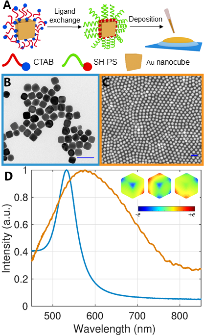
In solutions of low particle concentration, the inter-particle distances between neighboring particles is much larger than the near-fields generated by individual particle plasmons. Consequently, the optical properties of these particles are well-described by considering the interaction of an isolated nanocube with an incident light field. This interaction excites localized surface plasmon resonances, creating a surface charge distribution . Given that the nanoparticle dimensions are significantly smaller than the wavelength of visible light, this charge distribution can be written in terms of the (electrostatic) eigenmodes (or self-sustained oscillations) of the particle according to , where are the excitation amplitudes that describe the coupling of the incident light field with a particular eigenmode (here is an index that indicates the -th mode sustained by the nanoparticle). Modes with strong dipolar character couple strongly with uniform electric fields and thus have large values of . Consequently, these are manifest in optical extinction spectra, as shown in Figure 2D corresponding to Au nanocubes in Figure 2B. The calculated lowest-order (three-fold) degenerate eigenmodes of the nanocubes clearly have a strong dipolar character, with charge accumulation at each of the three orthogonal directions of the cube (Figure 2D inset). For these particles, the electrostatic eigenmode description (particles in a uniform medium with the refractive index of water; eigenvalue for this mode 1.728) predicts that these dipole resonances occur at 560 nm, which is in good agreement with the experimental value.
Plasmene is formed by the deposition of a chloroform solution of Au nanoparticles onto the surface of a water droplet. A change in polarity resulting from the evaporation of the chloroform results in self-assembly into an extended two-dimensional array on the surface of the water droplet, with subsequent evaporation yielding a quasi-crystalline lattice of plasmene 23 (Figure 2A, more detail in the Methods Section). The extinction spectrum () of a plasmene layer on a glass surface clearly demonstrates a strong modification to the nanostructures’ interaction with light (Figure 2D). This results from a combination of at least two effects: the interaction of the nanoparticles with a flat substrate, as well as inter-nanoparticle interactions. When the nanocubes are placed on a substrate, the degeneracy of the dipolar modes shown in Figure 2D is lifted, leading to hybridisation between bright (dipolar) and dark (multipolar) plasmon modes. In the case of Ag nanocubes, it has been shown that this results in substantial spectral red-shifts and the emergence of resonances that were absent in the solution spectrum 24, 25.
Inter-nanoparticle interactions also lead to plasmon hybridization 26; the surface electron charge oscillations that result from the interaction with light are delocalized over the array of particles. This forms a collective plasmon mode with a resonance frequency red-shifted with respect to that of the isolated particle.
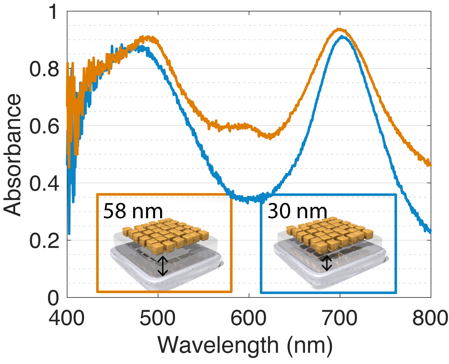
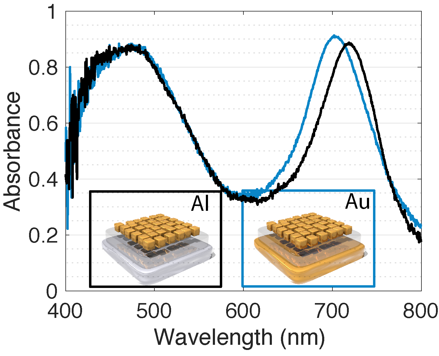
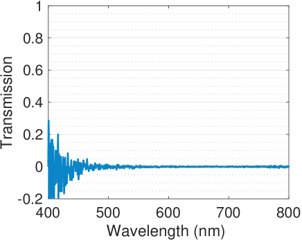
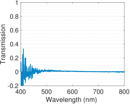
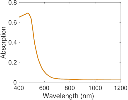
To experimentally realize plasmene near-perfect absorbers of light, the mirror and spacer layer were deposited by physical vapor deposition. The spacer layer consisted of TiO2, a dielectric with a high refractive index that is transparent to visible light. Self-assembly of a plasmene sheet on the TiO2 thin film completed the structure. Figure 3A shows the measured absorption spectra of two samples constructed using Al as the mirror, Au nanocubes as the plasmene building blocks, and TiO2 of different thicknesses. These spectra were determined by measuring the transmission () and reflection () spectra of each sample (the latter carefully referenced to a surface with a known reflectance spectrum), giving the absorption () as: by virtue of the conservation of energy (more detail in the Methods Section, the transmission spectra are shown in Figure S.1). With a dielectric spacer of 30 nm thickness, the spectrum showed two dominant absorption bands at 480 and 703 nm reaching absorption magnitudes of 86% and 91%, respectively. Increasing the dielectric spacer thickness to 58 nm slightly improved the maximum absorption to 94% at 700 nm. Interestingly, whilst the absorption band at 700 nm underwent a slight hypsochromic shift, the higher energy band (480–500 nm) showed a bathochromic shift as the TiO2 thickness increased, consistent with a distance-dependent interaction between the plasmene sheet and the metal layer 15. Changing the chemical composition of the mirror layer in the NPA from Al to Au caused a hypsochromic shift in the low energy absorption band (approx. 10 nm) along with a small increase in magnitude (Figure 3B). When compared to the extinction spectrum of a nanocube plasmene sheet deposited on glass (Figure 2C), the absorption bands of Figures 3 are noticeably sharper.
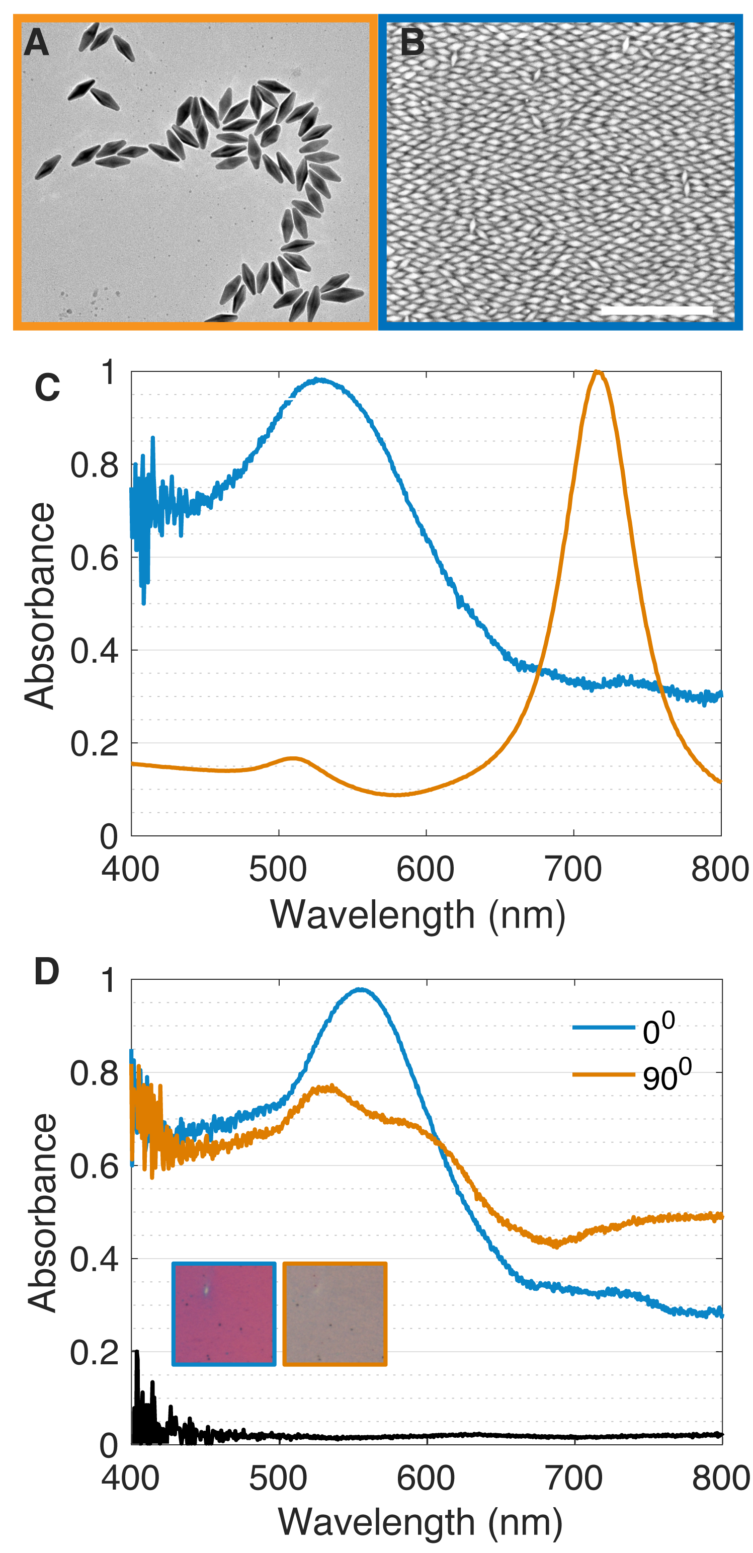
The absorption spectrum of plasmene is spectrally tailored by the geometry of the nanoparticle building blocks. This effect is illustrated in Figure 4, where we show NPAs made with bipyramidal-shaped Au nanocrystals. Due to their long aspect ratio (Figure 4A), Au bipyramid nanoparticles exhibit multiple localized surface plasmon resonances (Figure 4C). A plasmene NPA incorporating bipyramidal building blocks exhibited an absorption band with a maximum of 98% incident light absorption at 524 nm. (A second absorption band is expected to occur at higher wavelengths, beyond the detection range of the instrumentation used). Nanobipyramids can self-assemble to form plasmene sheets in four different packing orders 21, and due to their high structural aspect ratio, these assemblies can form plasmene sheets with optical properties that are sensitive to the polarization of the incident electromagnetic field (Figure 4D). These changes are also clearly visible to the naked eye under an optical microscope (Figure 4D inset).
The scattering of light imposes a lower limit on the reflectivity at the peak absorption. Scattering can occur as a consequence of structural disorder or the existence of edges in the plasmene lattice. The former may arise from the size distribution of the building blocks, whilst the latter may occur due to the finite extent of the plasmene sheets or the unintentional formation of stacked multiple layers. Figure 4(D) shows a comparison between the measured absorption and dark-field scattering spectra of a plasmene near-perfect absorber, which were measured against surfaces of known reflectance and calibrated scattering amplitude, respectively. The figure shows clearly that scattering amounts to 1% of the total incident power, indicating that it is strongly suppressed due to the regular ordering of the nanocrystal building blocks in the plasmene layer 14.
Theory For metasurfaces with a nanostructured layer, in which the inter-particle spacings are larger than the spatial extent of the plasmonic near-fields, perfect absorption has been modelled with a coupled-mode theory 27, 28, wherein each individual mirror-coupled nanocube reacts like a magnetic dipole. The collective action of an ensemble of these nanocubes results in an effective magnetic response, which enables almost complete impedance matching between the metasurface and free space, resulting in near-perfect absorption 14, 15, 8. In metasurfaces with a sparse surface coverage, these magnetic modes can be both excited and scattered at the edges of the nanocube, allowing for some of the radiation to escape and couple into free space.
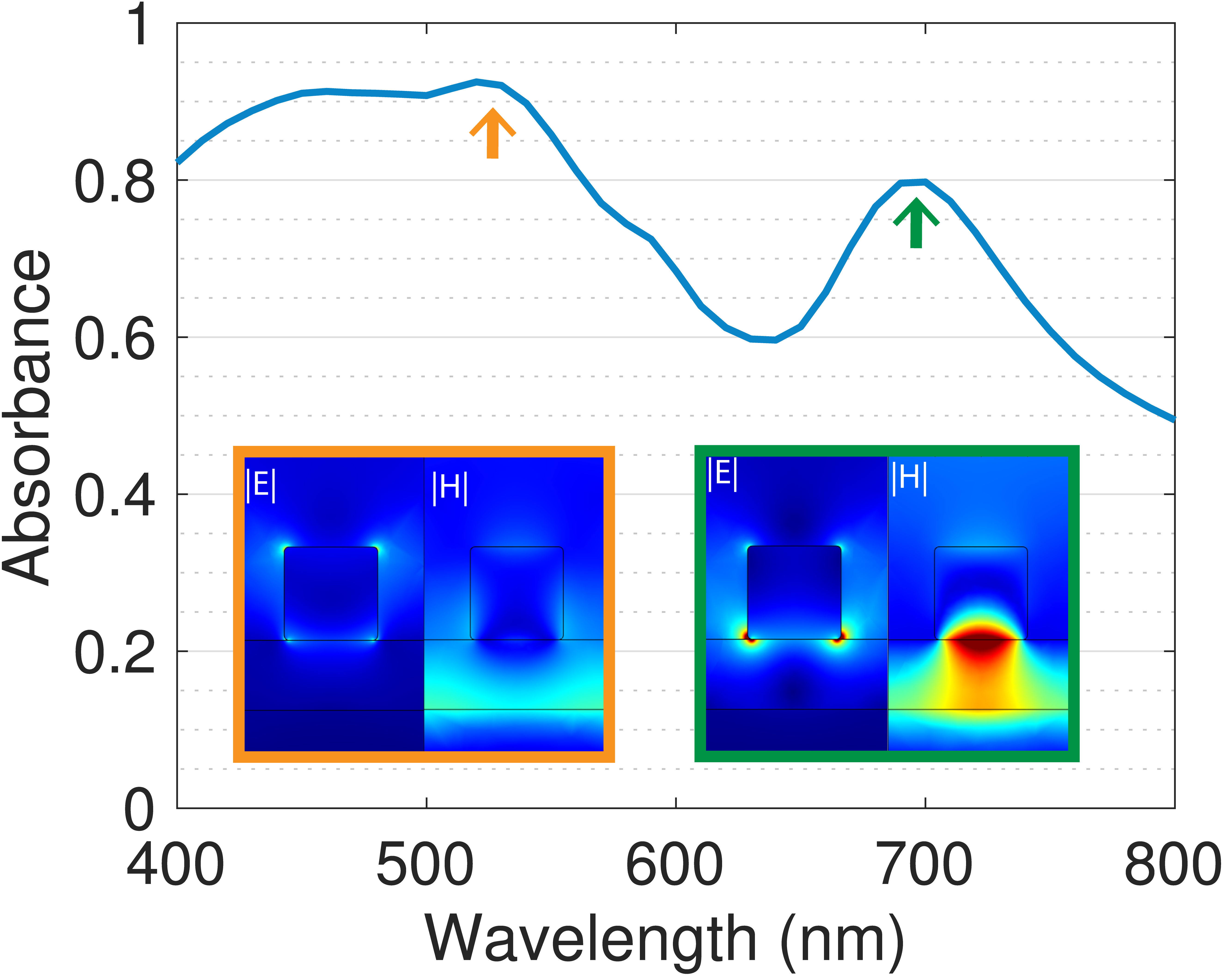
In order to gain a physical insight into the mechanism that enables almost complete impedance matching in plasmene NPAs, we have modelled the optical properties of a nanocube plasmene NPA using a finite element approach for solving Maxwell equations. The model material consisted of a periodic array of nanocubes of side length 40 nm ordered in a cubic lattice with a 100 nm period and a 30 nm spacer layer. Figure 5 shows the calculated absorption spectrum for this configuration with two bands that closely match the experimental data, along with the calculated maps of the magnitude of the electric () and magnetic () fields for each band. The electric field is strongly localized at the edges of the nanocube distant from the dielectric film, for the short–wavelength absorption band (located at 540 nm). For the long-wavelength absorption band (located at 700 nm), the electric field is strongly localized at the edges of the cube in contact with the dielectric film, and the magnetic field exhibits strong localization in the TiO2 layer, in a way similar to a magnetic dipole 3. This optical magnetic response originates from the interaction of the induced oscillating surface charges on the cube with their mirror images on the metal support. The radiation from the latter can cancel that produced by the induced dipole located on the nanoparticles, leading to suppression of reflection and causing the nanoparticles to absorb the energy, given that the mirror support prevents transmission of light 29. Given the deep sub-wavelength separation between the building blocks, the plasmene sheet can be rationalized to consist of an effective magnetic metasurface, that is different from a metal film of a similar thickness (see Figure S.2).
3 Conclusion
In summary, we have fabricated and measured the absorption spectra of plasmene near-perfect absorbers of light. We demonstrate that these materials can absorb up to 98% of incident visible light. The intense electromagnetic near-fields resulting from this near total extinction of light may find application in surface-enhanced spectroscopy, chemical and biological sensing, and plasmonic hot-carrier extraction. Notably, as the mirror and TiO2 layers can be deposited by solution-based approaches (such as electroplating, spin-coating and sol-gel methods), this report provides a pathway for the scalable, vacuum-free fabrication of NPAs.
4 Methods
Methods
Require a general materials section. Also, should note that all solutions are aq. unless otherwise noted, this is ambiguous.
Synthesis of Nanocrystal Building Blocks Synthesis of Au nanocubes A seed-mediated method was used to synthesize Au nanocubes 30.. Briefly, a seed solution was prepared by adding NaBH4 (0.6 ml, 0.01 M) to an aqueous solution prepared by mixing HAuCl4 (0.1 ml, 25 mM) and cetyltrimethylammonium bromide (CTAB) (7.65 ml, 0.1 M). The seed solution was then kept at 30 ∘C for 1 hour. The growth of Au nanocubes was triggered by adding 5 l of a 10-fold diluted seed solution into a growth solution prepared by adding CTAB (1.6 ml, 0.1 M), HAuCl4 (0.2 ml, 7 mM), and ascorbic acid (1.2 ml, 0.1 M) to Milli-Q water (8 ml). The resulting solution was then left undisturbed overnight, followed by centrifugation at 7830 rpm for 10 min and redispersal in Milli-Q water (10 ml) for further use.
Synthesis of Au Nanobipyramids (NBP) The synthesis of Au nanobipyramids involved a seed-meditated method and a three-step purification, as reported 21. A Au-seed solution was synthesized by adding NaBH4 (1 ml, 100 mM) to a solution prepared by adding HAuCl4 (0.4 ml, 25 mM) to aqueous trisodium citrate (40 ml, 0.25 mM). The resulting solution was then kept stirring at room temperature for 2 hours. Later, a portion of this seed solution (0.8 ml) was added to 100 ml of growth solution that contained aliquots of CTAB (0.1 M), HAuCl4 (2 ml, 25 mM), AgNO3 (1 ml, 10 mM), HCl (2 ml, 1.0 M), and ascorbic acid (0.8 ml, 0.1 M). The growth solution was kept at 30 °C overnight, and then centrifuged at 7830 rpm for 10 min, with the precipitate redispersed in an aqueous solution of CTAC (100ml, 80 mM). Purification of the Au NPBs was achieved using a three-step method reported previously 21. The final solution was washed and redispersed in Milli-Q water for further use.
Preparation of Metal-Semiconductor Substrates All films were deposited in an electron beam evaporation system (Intlvac, Nanochrome II) using a 10 kV power supply in a Class 10,000 cleanroom. Glass substrates were cleaned by sequential ultra-sonication in acetone and isopropanol, and then dried under a stream of nitrogen gas. The substrates were also cleaned by a plasma treatment step prior to the deposition of the metal-semiconductor films. In order to achieve good adhesion of the mirror layer to the substrate, a thin layer of Cr (5 nm, deposited 0.5 Å/s) was deposited. The Al or Au mirrors (100 nm, deposited 1.0 Å/s), and TiO2 spacer (30 or 60 nm, deposited 0.5 Å/s) were deposited sequentially. Dielectric film thickness was confirmed by spectroscopic ellipsometry (J. A. Woolam Co., M-2000DI).
Fabricated of Plasmene Sheets Plasmene was fabricated by a drying-mediated self-assembly method at an air-water interface 20. First, a two-step ligand-exchange method was used to replace CTAB ligands with thiol-terminated polystyrene (SH-PS) (Mn=50,000 for Au nanocubes and 20,000 for NBP). Briefly, 10 ml of the CTAB-capped Au nanocube solution (or 12 ml of the Au NBP solution) was centrifuged and redispersed in 5 ml (or 6 ml for Au NBP) SH-PS-THF (4 mg/ml) solution. The solution was then kept at room temperature overnight and purified by repeated centrifugation-precipitation cycles to remove uncapped ligands and precipitate the SH-PS capped nanoparticles. Finally, the solution was concentrated and redispersed in a small amount of chloroform. To assemble a plasmene sheet, one drop of nanoparticle solution was deposited onto a water droplet sitting on the mirror/spacer substrate. After the full evaporation of the water and chloroform, a plasmene sheet was obtained.
Characterization Normal incidence images of the resulting structures were obtained by scanning electron microscopy (FEI, NovaNanoSEM 430). SEM images of plasmene were obtained by a FEI Helios Nanolab 600 FIB-SEM operating at 5 kV.
Optical Measurements The optical transmission and reflectance spectra of the NPA plasmene sheets were measured using an upright microscope (Nikon LV100), coupled to a spectrograph (Andor, SR-303i-A) equipped with a CCD (iDUS DU420A-BEX2-DD). For all the measured spectra, the light source was a broadband 100 W halogen lamp. The illumination and collection of reflectance () was done with a objective (NA 0.55), and these measurements were referenced to a mirror with a known reflectance spectrum (Thorlabs BB1-E02). The transmission () spectra were calibrated using a bare glass substrate. The absorption data shown in this paper were calculated as: and are consequently not arbitrary values 10. Scattering spectra were measured using the same objective but placing a dark-field iris in front of the light source. These spectra were referenced to a white diffuse Reflectance Standard (Labsphere, Spectralon SRS-99-020).
Numerical Simulations The numerical simulations shown in Figure 5 were undertaken using the Finite Element Method implemented in COMSOL Multiphysics 5.3a. We used tabulated data for the refractive index of Au 31 and Al 32 for the substrate, and 1.0 for the medium above the structure. The refractive index of the TiO2 layer was assumed to be 2.4. Periodic boundary conditions were assumed on the sides and a port boundary was used at the excitation surface. The normally incident plane was assumed to be linearly polarised parallel to one of the horzontal edges of the cubes. The other surface of the model adjacent to the Al was taken to be a scattering boundary. No apparent backscattering from the terminating boundaries was apparent. The cubes were rounded to have a radius of curvature of 2 nm.
Acknowledgements This work was performed in part at the Melbourne Centre for Nanofabrication (MCN) in the Victorian Node of the Australian National Fabrication Facility (ANFF). We acknowledge the ARC for support through a Future Fellowship (FT140100514) and a Discovery Project (DP160100983).
Competing financial interests The authors declare no competing financial interests
References
- Yu et al. 2010 Yu, Z.; Raman, A.; Fan, S. Proceedings of the National Academy of Sciences 2010, 107, 17491–17496
- Polman and Atwater 2012 Polman, A.; Atwater, H. A. Nat Mater 2012, 11, 174–177
- Liu et al. 2010 Liu, N.; Mesch, M.; Weiss, T.; Hentschel, M.; Giessen, H. Nano Letters 2010, 10, 2342–2348
- Chen et al. 2012 Chen, K.; Adato, R.; Altug, H. ACS Nano 2012, 6, 7998–8006, PMID: 22920565
- Bossard et al. 2014 Bossard, J. A.; Lin, L.; Yun, S.; Liu, L.; Werner, D. H.; Mayer, T. S. ACS Nano 2014, 8, 1517–1524
- Rozin et al. 2015 Rozin, M. J.; Rosen, D. A.; Dill, T. J.; Tao, A. R. Nature Communications 2015, 6, 7325 EP –
- Hägglund et al. 2013 Hägglund, C.; Zeltzer, G.; Ruiz, R.; Thomann, I.; Lee, H.-B.-R.; Brongersma, M. L.; Bent, S. F. Nano Letters 2013, 13, 3352–3357, PMID: 23805835
- Akselrod et al. 2015 Akselrod, G. M.; Huang, J.; Hoang, T. B.; Bowen, P. T.; Su, L.; Smith, D. R.; Mikkelsen, M. H. Advanced Materials 2015, 27, 8028–8034
- Hedayati et al. 2011 Hedayati, M. K.; Javaherirahim, M.; Mozooni, B.; Abdelaziz, R.; Tavassolizadeh, A.; Chakravadhanula, V. S. K.; Zaporojtchenko, V.; Strunkus, T.; Faupel, F.; Elbahri, M. Advanced Materials 2011, 23, 5410–5414
- Aydin et al. 2011 Aydin, K.; Ferry, V. E.; Briggs, R. M.; Atwater, H. A. Nat Commun 2011, 2, 517
- Liu et al. 2015 Liu, Z.; Liu, X.; Huang, S.; Pan, P.; Chen, J.; Liu, G.; Gu, G. ACS Applied Materials & Interfaces 2015, 7, 4962–4968, PMID: 25679790
- Ng et al. 2016 Ng, C.; Cadusch, J.; Dligatch, S.; Roberts, A.; Davis, T. J.; Mulvaney, P.; Gomez, D. E. ACS Nano 2016, 10, 4704–4711
- Thongrattanasiri et al. 2012 Thongrattanasiri, S.; Koppens, F. H. L.; García de Abajo, F. J. Phys. Rev. Lett. 2012, 108, 047401
- Moreau et al. 2012 Moreau, A.; Ciraci, C.; Mock, J. J.; Hill, R. T.; Wang, Q.; Wiley, B. J.; Chilkoti, A.; Smith, D. R. Nature 2012, 492, 86–89
- Lassiter et al. 2013 Lassiter, J. B.; McGuire, F.; Mock, J. J.; Ciracì, C.; Hill, R. T.; Wiley, B. J.; Chilkoti, A.; Smith, D. R. Nano Letters 2013, 13, 5866–5872, PMID: 24199752
- Ng et al. 2012 Ng, K. C.; Udagedara, I. B.; Rukhlenko, I. D.; Chen, Y.; Tang, Y.; Premaratne, M.; Cheng, W. ACS Nano 2012, 6, 925–934, PMID: 22176669
- Guo et al. 2014 Guo, P.; Sikdar, D.; Huang, X.; Si, K. J.; Su, B.; Chen, Y.; Xiong, W.; Yap, L. W.; Premaratne, M.; Cheng, W. The Journal of Physical Chemistry C 2014, 118, 26816–26824
- Si et al. 2014 Si, K. J.; Sikdar, D.; Chen, Y.; Eftekhari, F.; Xu, Z.; Tang, Y.; Xiong, W.; Guo, P.; Zhang, S.; Lu, Y.; Bao, Q.; Zhu, W.; Premaratne, M.; Cheng, W. ACS Nano 2014, 8, 11086–11093, PMID: 25265019
- Si et al. 2015 Si, K. J.; Guo, P.; Shi, Q.; Cheng, W. Analytical Chemistry 2015, 87, 5263–5269, PMID: 25860874
- Shi et al. 2018 Shi, Q.; Dong, D.; Si, K. J.; Sikdar, D.; Yap, L. W.; Premaratne, M.; Cheng, W. ACS Nano 2018, 12, 1014–1022, PMID: 29303252
- Shi et al. 2016 Shi, Q.; Si, K. J.; Sikdar, D.; Yap, L. W.; Premaratne, M.; Cheng, W. ACS Nano 2016, 10, 967–976, PMID: 26731313
- Davis and Gómez 2017 Davis, T. J.; Gómez, D. E. Reviews of Modern Physics 2017, 89, 011003
- Bauer et al. 2011 Bauer, C.; Kobiela, G.; Giessen, H. Phys. Rev. B 2011, 84, 193104
- Sherry et al. 2005 Sherry, L. J.; Chang, S.-H.; Schatz, G. C.; Van Duyne, R. P.; Wiley, B. J.; Xia, Y. Nano Letters 2005, 5, 2034–2038, PMID: 16218733
- Zhang et al. 2011 Zhang, S.; Bao, K.; Halas, N. J.; Xu, H.; Nordlander, P. Nano Letters 2011, 11, 1657–1663
- Prodan et al. 2003 Prodan, E.; Radloff, C.; Halas, N. J.; Nordlander, P. Science 2003, 302, 419–422
- Ciracì et al. 2013 Ciracì, C.; Lassiter, J. B.; Moreau, A.; Smith, D. R. Journal of Applied Physics 2013, 114, 163108
- Bowen and Smith 2014 Bowen, P. T.; Smith, D. R. Phys. Rev. B 2014, 90, 195402
- Chen 2012 Chen, H.-T. Opt. Express 2012, 20, 7165–7172
- Qianqian et al. 2018 Qianqian, S.; Debabrata, S.; Runfang, F.; Jye, S. K.; Dashen, D.; Yiyi, L.; Malin, P.; Wenlong, C. Advanced Materials 2018, 1801118
- Johnson and Christy 1972 Johnson, P. B.; Christy, R. W. Phys. Rev. B 1972, 6, 4370–4379
- Rakić et al. 1998 Rakić, A. D.; Djurišic, A. B.; Elazar, J. M.; Majewski, M. L. Applied Optics 1998, 37, 5271–5283