Planar Superconductor-Ferromagnet-Superconductor Josephson junctions as scanning probe sensors.
Abstract
We propose a novel type of magnetic scanning probe sensor, based on a single planar Josephson junction with a magnetic barrier. The planar geometry together with high magnetic permeability of the barrier helps to focus flux in the junction and thus enhance the sensitivity of the sensor. As a result, it may outperform equally sized SQUID both in terms of the magnetic field sensitivity and the spatial resolution in one scanning direction. We fabricate and analyze experimentally sensor prototypes with a superparamagnetic CuNi and a ferromagnetic Ni barrier. We demonstrate that the planar geometry allows easy miniaturization to nm-scale, facilitates an effective utilization of the self-field phenomenon for amplification of sensitivity and a simple implementation of a control line for feed-back operation in a broad dynamic range.
pacs:
85.25.Cp 74.50.+r 74.45.+cSuperconducting Quantum Interference Devices (SQUIDs) are the most sensitive magnetic sensors, capable of measuring a small fraction of the flux quantum Wb Koelle_1999Rev ; Kirtley_1999Rev . In recent two decades SQUID sensors have been successfully employed in scanning-probe microscopes with a variety of different designs and operation modes Kirtley_1999Rev ; Bouchiat_2009Rev ; Granata_2016Rev ; Zeldov_2013 ; Tzalenchuk_2003 ; Moler_2017 . The main challenge in scanning SQUID microscopy is a tradeoff between the field sensitivity and the spatial resolution. Usually a dc-SQUID, a loop with two junctions, is used for such applications. For a loop with the area , the magnetic field sensitivity is determined by the ratio while the spatial resolution is determined by the loop size and the distance between the loop and the sample. For increasing spatial resolution, nano-SQUIDs can be used Bouchiat_2009Rev ; Granata_2016Rev ; Zeldov_2013 ; Tzalenchuk_2003 , but at the expense of reduced sensitivity. In the conventional flat geometry of the SQUID, the miniaturization is limited by the required minimum critical current A for avoiding thermal fluctuations at the operation temperature of several K Anticorrelation_2007 . Since scales with the junction area, this limits the smallest junction size for a given critical current density and operation temperature. This can be obviated in a three-dimensional SQUID-on-a-tip geometry Zeldov_2013 . The complexity of the full scanning probe SQUID-sensor design Kirtley_1999Rev ; Moler_2017 , including the SQUID loop with two junctions and a feed-back loop, is also a hinder for miniaturization.
In recent years hybrid Superconductor-Ferromagnet (SF) devices are being actively studied. The competition between superconductivity and magnetism in SF heterostructures leads to new phenomena and functionality which is interesting for variety of novel electronic and spintronic components, Soloviev_2017 such as phase shifters Feofanov_2010 ; Golod_PRL2010 ; Pugach_2011 ; Birge_2016 , superconducting spin valves Khaire_2010 ; Leksin_2011 ; Banerjee_2014 ; Iovan_2014 ; Blamire_2017 ; Aarts_2017 , memory cells Bolginov_2012 ; Dresselhaus_2014 ; Golod_2015 ; Birge_2018 .
Here we propose a novel type of magnetic scanning probe sensor, based on a single planar Josephson junction with a magnetic barrier. We fabricate and analyze experimentally Nb/CuNi/Nb and Nb/Ni/Nb sensor prototypes with a paramagnetic CuNi and a ferromagnetic Ni barrier. We show that field sensitivity of such a sensor may exceed the sensitivity of equally-sized SQUID. This is caused by a double flux-focusing effect in a planar SFS junction: first, due to a large demagnetization factor of S-electrodes in a perpendicular magnetic field, and second, due to a large magnetic permeability of the F-barrier. Furthermore, we argue that such a sensor can provide a better than SQUID spatial resolution in one scanning direction. The two-dimensional planar geometry with just one junction and no loop allows a flexible design, straightforward miniaturization to nm-scale and effective utilization of self-field phenomenon for amplification of sensitivity. We test scaling of the device down to 200 nm size and suggest and verify several modifications of the sensor for enhancing its performance, including usage of several junctions in series for increasing the readout signal and a control-line for feed-back operation at the point of maximum sensitivity with a broad dynamic range. We argue that the combination of high field sensitivity, high spatial resolution in one direction and simple and flexible 2D design makes planar SFS junctions beneficial for usage as scanning probe sensors.
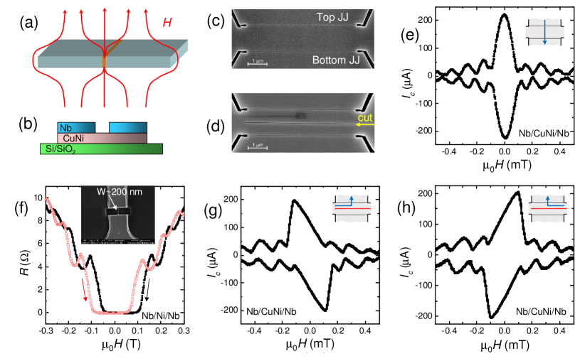
Planar Josephson junctions (JJs) are formed at the edge between two superconducting films, see Figure 1 (a). They differ significantly from conventional overlap (sandwich-type) junctions. In particular, electrodynamics of planar junctions is nonlocal when electrode thickness is less than the London penetration depth Ivanchenko ; MintsJLTP1997 ; Kogan2001 ; Boris_2013 . When magnetic field is applied perpendicular to the film plane, Meissner screening leads to spreading of magnetic field lines along the surface, as sketched in Fig. 1(a). This causes flux-focusing in the junction barrier Mints2008 ; Clem2011 , which greatly enhances sensitivity of the planar junction to magnetic field. The figure of merit for field sensitivity is the field for achieving a flux quantum. For the symmetric planar junction with two identical electrodes of sizes (WidthLength) the quantization field is Clem2011
| (1) | |||
| (2) |
It has to be compared to the quantization field of the SQUID . Note that here and are width and length to the mid-points of the SQUID loop electrodes, while in planar junctions the full width and length play role. The relative difference is increasing with decreasing sizes. In case of nanoscale sensors this can be an additional factor in favor of planar junctions. This comparison indicates that the field sensitivity of planar junctions is comparable to that for similarly sized SQUIDs. Furthermore, we anticipate that SFS planar junctions can outperform SQUIDs due to additional flux focusing in the F-barrier with high magnetic permeability Gudoshnikov_2001 . This is the main motivation for our work.
SFS planar junctions are made by focused ion beam (FIB) etching of a narrow grove through an SF bilayer film Blamire_1999 ; PhysicaC_2005 , as sketched in Fig. 1 (b). Details of junction fabrication and characterization can be found in Refs. PhysicaC_2005 ; Anticorrelation_2007 ; Golod_PRL2010 ; Golod_2015 . The fabrication procedure is simple and reproducible. Junctions are very stable, no deterioration occurred over five year storage at ambient conditions.
Fig. 1 (c) represents a scanning electron microscope (SEM) image of the device, made from Nb/Cu1-xNix ( bilayer. Thin CuNi films have perpendicular magnetic anisotropy Veshchunov_2008 , which in combination with high magnetic permeability, helps to additionally focus perpendicular magnetic field in the planar junction and, thus, further increases the field sensitivity. The superparamagnetic Cu1-xNix alloy with Ni concentration close to the critical for ferromagnetism is chosen to avoid hysteresis of detector characteristics, which deteriorates the detector performance Gudoshnikov_2001 . Furthermore, such CuNi alloys have a large resistivity, which lifts the junction resistance to a comfortably measurable value;
The device in Fig. 1 (c) contains two planar Nb/CuNi/Nb junctions (marked top and bottom JJ) with similar characteristics. The junction width is and the separation between them is . There are four long electrodes (top, bottom, left, right) with two bonding pads for each, allowing independent as well as serial biasing of the junctions and measurements in the four-probe configuration. After initial tests, an additional separating FIB cut down to the substrate was made between the junctions, marked by an arrow in Fig. 1 (d), to test possible improvements of the sensor. It is seen that the Nb/CuNi/Nb junctions have dissimilar electrodes. The outer is much longer than the width and the inner electrode between the junctions is shorter . Each of them should provide half of the flux from Eqs.(1) and (2), correspondingly, because those equations were obtained for symmetric junctions with additive contribution from two equal electrodes. Therefore the anticipated effective quantization area for our junctions is m2.
Fig. 1 (e) shows magnetic field dependence of the critical current for the top junction (the bottom junction exhibits similar characteristics). Measurements are done at K, before making the separating FIB cut. In this case the current was sent uniformly through both junctions, straight from top to bottom electrodes, as sketched in the inset. A regular Fraunhofer-like modulation indicates good uniformity of JJs. The does not exhibit hysteresis, confirming that the CuNi layer is in the superparamagnetic state. The flux quantization field is Oe, yielding the effective quantization area m2. It is two times larger than the value anticipated from the junction geometry. We ascribe the corresponding improvement in sensitivity to additional field-focusing contribution of the CuNi barrier.
The simple two-dimensional (2D) geometry of a planar sensor with just one junction allows straightforward miniaturization to nano-scale. To check the scalability and the effect of ferromagnetism in the junction, we fabricated a junction with the width nm, containing pure Ni, which is a strong ferromagnet. Inset in Fig. 1 (f) shows a SEM image of the Nb/Ni/Nb junction. The main panel in Fig. 1 (f) shows zero-bias ac-resistance of the junction for upward and downward sweep of magnetic field at K. A hysteresis due to coercivity of ferromagnetic Ni is clearly seen. The modulation reflects the modulation: minima/maxima of correspond to maxima/minima of Iovan_2014 . The Fraunhofer-type modulation of is seen. The period kOe is in agreement with Eq. (1) for nm. This confirms that miniaturization of planar junction detectors to nm scale is indeed simple, but it is accompanied by the inevitable deterioration of the field sensitivity. It is also clear that the ferromagnetic barrier introduced the hysteresis in the detector characteristics, which is detrimental for its operation Gudoshnikov_2001 . Therefore, below we will focus on analysis of micron-sized planar detectors with the superparamagnetic CuNi barrier.
The 2D planar geometry allows a flexible design and in-situ tuning of junction characteristics. Figures 1 (g) and (h) show patterns of the top junction with the bias current sent (g) from the left to the top electrode and (h) from the right to the top electrode, as sketched in insets. It is seen that the patterns are distorted compared to the straight uniform bias case in Fig. 1 (e). The distortion is caused by the self-field effect induced by unevenly distributed bias current Vasenko_1981 ; Barone ; Krasnov_1997 . The sign of self-field depends on the direction of the bias current and reverts between Figs. 1 (g) and (h), demonstrating in-situ tunability of junction characteristics. Importantly, the self-field effect leads to a significant sharpening of at one of the slopes of the central lobe. This greatly enhances the field sensitivity. For the bias configuration in Figs. 1 (g,h) the easy to detect A variation of at the sharp slope corresponds to field and flux variation in mOe and ranges, respectively.
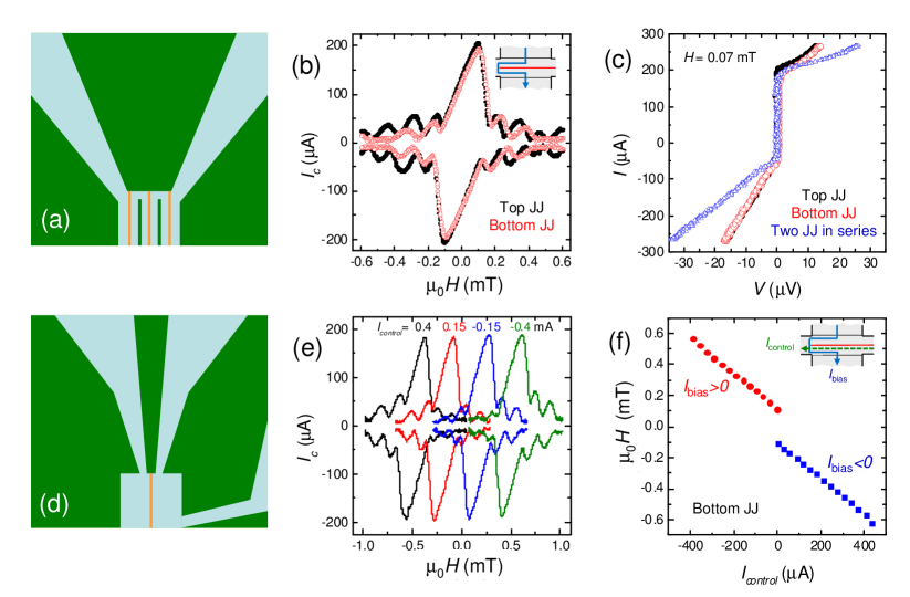
Our junctions have a rather small V, which determines the voltage readout. It is possible to tune it in a broad range by changing the FIB cut depth PhysicaC_2005 . Alternatively it can be multiplied by serial arrangement of several junctions, as sketched in Figure 2 (a). In order to facilitate the self-field in this case we suggest to make separating cuts between the junctions. In this case the bias current from left to right electrode will have to flow vertically along the junction lines, which induces self-field in the junctions. The studied sample allows to test this idea since it contains two junctions. Fig. 2 (b) shows patterns of both junctions at K, measured after making the separating cut, marked in Fig. 1 (d). The bias current is sent from the top to the bottom electrode, just like in the case of Fig. 1 (d), see the sketch in Fig. 2 (b). However, presence of the cut induces the desired self-field distortion of patterns. Simultaneously it does not deteriorate significantly the sensitivity, the flux quantization field Oe. Fig. 2 (c) shows corresponding - characteristics of individual junction and their serial sum at corresponding to maximum positive . It is seen that the of two junctions in series indeed doubles. We emphasize that such a multiplication of the output is a consequence of high reproducibility of the fabrication technique, which leads to nearly identical patterns for the two junctions, see Fig. 2 (b).
The planar geometry allows simple adjustment of the self-field effect and, thus, the field sensitivity. It increases with decreasing the angle and the gap between bias electrodes. With proper design can be made infinitely large. In Figure 2 (d) we sketch a corresponding simplest design on the sensor with two almost parallel electrodes and a small gap between them for enhancement of the self-field. The best sensitivity is achieved in a narrow field range with the maximum slope. Therefore, for optimal operation, the sensor should be kept at this point. In SQUIDS this is achieved by a separate feed-back loop Koelle_1999Rev ; Moler_2017 . In our planar detector this can be done in a simpler way by adding one additional electrode, as sketched in Fig. 2 (d). The third electrode attached to the bottom right side of the junction facilitate current flow along the junction (from top-right to bottom-right electrode). In this case the electrode itself acts as a control line for offsetting the sensor.
The studied Nb/CuNi/Nb sensor has four electrodes, see Fig. 1 (d). Therefore, we can use two of them (top and bottom) for sending the bias current and the other two (left and right) for sending the control current, . Fig. 2 (e) shows patterns of the bottom Nb/CuNi/Nb junction measured at four control currents. The bias and control current configurations are sketched in the inset in Fig. 2 (f). It is seen that the patterns are shifted by the control current. This allows the feedback operation of the sensor at the maximum sensitivity point within the field range of the corresponding shift by . Fig. 2 (f) shows the corresponding shift of the maxima at central lobes for positive (circles) and negative (squares) bias currents as a function of the control current. The linear shift demonstrates the dynamic range of the feedback operation by the control current of Oe, corresponding to in the junction for this particular device. This means, that upon scanning of a sample, the sensor will be able to measure signals in the broad range in a feedback mode with the maximum field sensitivity.
Finally, we discuss the spatial resolution of the proposed scanning probe sensor. In the direction along the junction the spatial resolution in determined by the size (electrode width), similar to SQUID sensors. However in the direction perpendicular to the junction line, the spatial sensitivity may be amplified by flux focusing in the narrow barrier with high magnetic permeability. Therefore, we anticipate that the planar SFS junction can outperform similar-sized SQUID in terms of spatial resolution in one scanning direction.
To conclude, we have proposed a novel type of magnetic sensor, based on a single planar SFS Josephson junction. We have verified it experimentally using a superparamagnetic CuNi alloy and a strong ferromagnet Ni as a barrier material. We have shown that a simple planar geometry facilitates a flexible design of the sensor and in-situ tuning of its characteristics. This allows utilization of the self-field effect for significant amplification of sensitivity, a feed-back operation in a broad dynamic range using junction electrodes as a control line, and employment of several junction in series for enhancing the voltage readout. We also demonstrated a possibility of down-scaling of the device to 200 nm, which, however, inevitably leads to reduction of field sensitivity, as for small SQUIDs. We concluded that proposed planar junction scanning probe sensors may outperform similar-sized SQUIDs both in terms of spatial resolution in the scanning direction perpendicular to the junction line and in terms of field sensitivity, due to two flux-focusing effects: a large demagnetization factor of S-films in perpendicular field and a large magnetic permeability of the magnetic barrier. We argue that the combination of high field sensitivity, high spatial resolution in one direction and simple and flexible 2D design makes planar SFS junctions beneficial for usage as scanning probe sensors.
References
- (1) D. Koelle, R. Kleiner, F. Ludwig, E. Dantsker, and J. Clarke. High-transition-temperature superconducting quantum interference devices. Rev. Mod. Phys. 71, 631–686 (1999).
- (2) J. R. Kirtley and J.P. Wikswo, Jr. Scanning SQUID Microscopy. Annu. Rev. Mater. Sci. 29, 117-148 (1999).
- (3) P. Josephs-Franks, L. Hao, A. Tzalenchuk, J. Davies, O. Kazakova, J. C. Gallop, L. Brown and J. C. Macfarlane. Measurement of the spatial sensitivity of miniature SQUIDs using magnetic-tipped STM. Supercond. Sci. Technol. 16, 1570–1574 (2003).
- (4) V. Bouchiat. Detection of magnetic moments using a nano-SQUID: limits of resolution and sensitivity in near-field SQUID magnetometry. Supercond. Sci. Technol. 22, 064002 (2009).
- (5) Z. Cui, J. R. Kirtley, Y. Wang, P. A. Kratz, A. J. Rosenberg, C. A. Watson, G. W. Gibson Jr., M. B. Ketchen, and K. A. Moler. Scanning SQUID sampler with 40-ps time resolution. Rev. Sc. Instr. 88, 083703 (2017).
- (6) C. Granata and A. Vettoliere. Nano Superconducting Quantum Interference device: A powerful tool for nanoscale investigations. Phys. Rep. 614, 1–69 (2016).
- (7) D. Vasyukov, et al. A scanning superconducting quantum interference device with single electron spin sensitivity. Nature Nanotechn. 8, 639 (2013).
- (8) V.M. Krasnov, T.Golod, T. Bauch, and P. Delsing. Anticorrelation between temperature and fluctuations of the switching current in moderately damped Josephson junctions. Phys. Rev. B 76, 224517 (2007).
- (9) I. I. Soloviev, N. V. Klenov, S. V. Bakurskiy, M. Yu. Kupriyanov, A. L. Gudkov, and A. S. Sidorenko. Beyond Moore s technologies: operation principles of a superconductor alternative. Beilstein J. Nanotechnol. 8, 2689 -2710 (2017).
- (10) A.K. Feofanov, et al. Implementation of superconductor/ferromagnet/superconductorpi-shifters in superconducting digital and quantum circuits. Nature Phys. 6, 593–597 (2010).
- (11) T. Golod, A. Rydh, and V.M. Krasnov. Detection of the Phase Shift from a Single Abrikosov Vortex. Phys. Rev. Lett. 104, 227003 (2010).
- (12) D.M. Heim, N.G. Pugach, M.Yu. Kupriyanov, E. Goldobin, D. Koelle, D, and R. Kleiner. Ferromagnetic planar Josephson junction with transparent interfaces: a phi junction proposal. J. Phys. Cond. Mat. 25, 215701 (2013).
- (13) E. C. Gingrich, B. M. Niedzielski, J. A. Glick, Y. Wang, D. L. Miller, R. Loloee, W. P. Pratt Jr., and N. O. Birge. Controllable Josephson junctions containing a ferromagnetic spin valve. Nature Phys. 12, 564–569 (2016).
- (14) T.S. Khaire, M.A. Khasawneh, W.P. Pratt, Jr., and N.O. Birge. Observation of Spin-Triplet Superconductivity in Co-Based Josephson Junctions. Phys. Rev. Lett. 104, 137002 (2010).
- (15) P. V. Leksin, N. N. Garif yanov, I. A. Garifullin, J. Schumann, V. Kataev, O. G. Schmidt, and B. Büchner. Manifestation of New Interference Effects in a Superconductor-Ferromagnet Spin Valve. Phys. Rev. Lett. 106, 067005 (2011).
- (16) A. Iovan, T. Golod, and V. M. Krasnov. Controllable generation of a spin-triplet supercurrent in a Josephson spin valve. Phys. Rev. B 90, 134514 (2014).
- (17) N. Banerjee, C.B. Smiet, R.G.J. Smits, A. Ozaeta, F.S. Bergeret, M.G. Blamire and J.W.A. Robinson. Evidence for spin selectivity of triplet pairs in superconducting spin valves. Nature Commun. 5, 3048 (2014).
- (18) Y. Zhu, A. Pal, M. G. Blamire and Z. H. Barber. Superconducting exchange coupling between ferromagnets. Nature Mat. 16, 195–199 (2017).
- (19) K. Lahabi, M. Amundsen, J. A. Ouassou, E. Beukers, M. Pleijster, J. Linder, P. Alkemade, and J. Aarts. Controlling supercurrents and their spatial distribution in ferromagnets. Nature Commun. 8, 2056 (2017).
- (20) T.E. Golikova, F. Huebler, D. Beckmann, I.E. Batov, T.Yu. Karminskaya, M.Yu. Kupriyanov, A.A. Golubov, and V.V. Ryazanov. Double proximity effect in hybrid planar superconductor-(normal metal/ferromagnet)-superconductor structures. Phys. Rev. B 86, 064416 (2012).
- (21) B. Baek, W.H. Rippard, S.P. Benz, S.E. Russek, and P.D. Dresselhaus. Hybrid superconducting-magnetic memory device using competing order parameters. Nat. Commun. 5, 3888 (2014).
- (22) T. Golod, A. Iovan, and V. M. Krasnov. Single Abrikosov vortices as quantized information bits. Nature Commun. 6, 8628 (2015).
- (23) B. M. Niedzielski, T. J. Bertus, J. A. Glick, R. Loloee, W. P. Pratt, Jr., and N. O. Birge. Spin-valve Josephson junctions for cryogenic memory. Phys. Rev. B 97, 024517 (2018).
- (24) Y.M. Ivanchenko and T.K. Soboleva. Nonlocal interaction in Josephson junctions. Phys. Lett. A 147, 65 (1990).
- (25) R.G. Mints. Nonlocal Josephson Electrodynamics. J. Low Temp. Phys. 106, 183 (1997).
- (26) V.G. Kogan, V.V. Dobrovitski, J.R. Clem, Y. Mawatari, and R.G. Mints. Josephson junction in a thin film. Phys. Rev. B 63, 144501 (2001).
- (27) A. A. Boris, A. Rydh, T. Golod, H. Motzkau, A. M. Klushin, and V. M. Krasnov. Evidence for Nonlocal Electrodynamics in Planar Josephson Junctions. Phys. Rev. Lett. 111, 117002 (2013).
- (28) M. Moshe, V.G. Kogan, and R.G. Mints. Edge-type Josephson junctions in narrow thin-film strips. Phys. Rev. B 78, 020510(R) (2008).
- (29) J.R. Clem. Josephson junctions in thin and narrow rectangular superconducting strips. Phys. Rev. B 81, 144515 (2010).
- (30) S. A. Gudoshnikov, Y. V. Deryuzhkina, P. E. Rudenchik, Y. S. Sitnov, S. I. Bondarenko, A. A. Shablo, P. P. Pavlov, A. S. Kalabukhov, O. V. Snigirev, and P. Seidel. Magnetic flux guide for high-resolution SQUID microscope. IEEE Trans. Appl. Supercond. 11, 219-222 (2001).
- (31) R.W. Moseley, W.E. Booij, E.J. Tarte, M.G. Blamire. Direct writing of low superconductor-normal metal-superconductor junctions using a focused ion beam. em Appl. Phys. Lett. 75, 262 (1999).
- (32) V.M. Krasnov, O. Ericsson, S. Intiso, P. Delsing, V.A. Oboznov, A.S. Prokofiev, and V.V. Ryazanov. Planar S F S Josephson junctions made by focused ion beam etching. Physica C 418, 16–22 (2005).
- (33) I.S. Veshchunov, V.A. Oboznov, A.N. Rossolenko, A.S. Prokofiev, L.Ya. Vinnikov, A.Yu. Rusanov and D.V. Matveev. Observation of the magnetic domain structure in Cu0.47Ni0.53 thin films at low temperatures. JETP Lett. 88, 758–761 (2008).
- (34) A. Barone and G. Paterno, Physics and Applications of the Josephson effect, A Wiley Intersc. Publ. (1982), ISBN 0-471-01469-9.
- (35) S. A. Vasenko, K. K. Likharev, and V. K. Semenov. Static properties of distributed inhomogeneous Josephson junctions. Sov. Phys. JETP 54, 766–771 (1981).
- (36) V.M. Krasnov, V.A. Oboznov, and N.F. Pedersen. Fluxon dynamics in long Josephson junctions in the presence of a temperature gradient or spatial nonuniformity. Phys. Rev. B 55, 14486–14498 (1997).