Growth and Structure of Singly-Oriented Single-Layer Tungsten Disulfide on Au(111)
Abstract
We present a complete characterization at the nanoscale of the growth and structure of single-layer tungsten disulfide (\ceWS2) epitaxially grown on Au(111). Following the growth process in real time with fast x-ray photoelectron spectroscopy, we obtain a singly-oriented layer by choosing the proper W evaporation rate and substrate temperature during the growth. Information about the morphology, size and layer stacking of the \ceWS2 layer were achieved by employing x-ray photoelectron diffraction and low-energy electron microscopy. The strong spin splitting in the valence band of \ceWS2 coupled with the single-orientation character of the layer make this material the ideal candidate for the exploitation of the spin and valley degrees of freedom.
I Introduction
Only a short time after the successful creation of graphene by mechanical exfoliation Novoselov et al. (2004, 2005a); Zhang et al. (2005), it was realized that other two-dimensional materials could be obtained in a similar way from layered crystals, especially transition metal dichalcogenides (TMDCs) Novoselov et al. (2005b). This has lead to an intense study of single layer (SL) TMDCs which, like graphene, show electronic properties that are remarkably different from those of their parent bulk compound. Initially, much attention had been given to the presence of a direct band gap in some of the semiconducting SL TMDCs Splendiani et al. (2010); Mak et al. (2010) and the possibility to exploit this property in electronic and opto-electronic applications Radisavljevic et al. (2011); Lopez-Sanchez et al. (2013). Later, it was suggested that these materials could be used for entirely new concepts in electronics because of their coupled spin Xiao et al. (2012) and valley Mak et al. (2012); Zeng et al. (2012); Cao et al. (2012); Mak et al. (2014) degrees of freedom Xu et al. (2014), something that does not play a role in graphene where inversion symmetry prevents the lifting of the spin degeneracy.
The technological exploitation of the SL TMDCs will benefit from production by bottom-up growth, rather than exfoliation. Chemical vapor deposition and molecular beam epitaxy appear to be promising approaches to obtain a high degree of orientation and a closed layer Lee et al. (2012); Shi et al. (2012); Li et al. (2015); Pyeon et al. (2016); Lehtinen et al. (2015); Chen et al. (2016); Fu et al. (2017); Kang et al. (2018) An additional requirement for devices that shall make use of the valley degree of freedom, such as a valley filter Rycerz et al. (2007), is to avoid the presence of mirror domains, a common defect in the growth of SL TMDCsLehtinen et al. (2015). The two mirrored versions of the SL TMDC unit cell have the same reciprocal lattice, with merely the K and -K points of the surface Brillouin zone inverted Bana et al. (2018) and the same band structure, apart from an inverted spin polarization for the two mirror domains. The presence of mirrored domains is thus detrimental for both fundamental studies on the coupled spin and valley degrees of freedom and for the use of TMDCs in devices Mak et al. (2014); Mak and Shan (2016).
There has been recent progress in the growth of single orientation two-dimensional materials, for example for SL BN on Ir(111) Orlando et al. (2014), as well as for SL MoS2 on hexagonal boron nitride Fu et al. (2017) and Au(111) Bana et al. (2018). Herein, we investigate the growth and structural features of epitaxially-grown SL \ceWS2 on Au(111). We reveal that a bottom-up approach can be employed to obtain SL \ceWS2 with a single orientation, a feature that has not been reported so far. This aspect, together with the spin-splitting in the valence band, which is one of the largest among TMDCs Zhu et al. (2011); Wang et al. (2012); Kormányos et al. (2015), opens up the possibility to investigate and exploit the coupled valley and spin degrees of freedom in devices applications. We characterize the samples by X-ray photoelectron spectroscopy (XPS) and determine the structural parameters and the extent and orientation of the crystalline domains by combining low-energy electron diffraction (LEED) and microscopy (LEEM) with X-ray photoelectron diffraction (XPD). XPD measurements were able to conclusively prove that SL \ceWS2 can grow with a single orientation and determine the relative orientation of SL \ceWS2 with respect to the Au(111) substrate.
II Experimental Methods
Growth and characterization experiments were carried out at the SuperESCA beamlineBaraldi et al. (2003) of the Elettra Synchrotron radiation facility in Trieste, Italy, except for the LEEM data, which were acquired at the University of Bremen. The Au(111) substrate was cleaned by cycles of \ceAr+ ion sputtering at 2 keV and annealing up to 950 K. Cleanliness of the surface was checked by LEED and XPS, which did not detect traces of contamination. High-resolution S and W core level spectra were measured at room temperature in normal emission on the as-grown WS2 single layer, using photon energies of 260 eV and 140 eV, respectively. The overall energy resolution was below 50 meV. Thanks to the combination of a high-flux beamline and a high-efficiency electron detector, it was possible to measure fast X-ray photoelectron spectroscopy (XPS) spectra during the growth, greatly aiding the optimization of growth parameters.
Each XPD pattern was measured by collecting XPS spectra for more than 1000 different polar () and azimuthal () angles, as defined in the diagram in Figure 2. For each of these spectra, a peak fit analysis was performed (parameters of the analysis reported in Supplementary Material) and the intensity , of each component resulting from the fit, i.e. the area under the photoemission line, was extracted. The resulting XPD patterns are the stereographic projection of the modulation function , which was obtained from the peak intensity for each emission angle as
| (1) |
where () is the average intensity for each azimuthal scan at polar angle . The structural determination was performed by comparing measured XPD patterns to multiple scattering simulations for a trial structure. Such patterns were simulated using the program package for Electron Diffraction in Atomic Clusters (EDAC)García de Abajo et al. (2001). The presence of two mirror domain orientations was taken into account by an incoherent superposition of the calculated intensities, based on the well-funded Grønborg et al. (2015); Dendzik et al. (2015a) assumption of domain sizes that are sufficiently large to neglect boundary effects. The agreement between the simulations and the experimental results was quantified by computing the reliability factor Woodruff (2007)
| (2) |
where and are the simulated and the experimental modulation functions for each emission angle . The estimation of the accuracy of the quantities derived by means of R-factor analysis, i.e. lattice constant, layer thickness and percentage of mirror domains, was deduced from the R-factor confidence interval defined as Pendry (1980)
| (3) |
where is the minimum R-factor value and is the number of well-resolved peaks in the XPD pattern . The LEED experiments were carried out using a commercial VG instrument installed at the experimental chamber of the SuperESCA beamline.
LEEM data were recorded using an ELMITEC LEEM III instrument at the University of Bremen. A sample was prepared at the SuperESCA beamline, transferred to Bremen through air and then annealed to 670 K after inserting it in the ultra-high vacuum (UHV) chamber. As a diffraction based method, LEEM can access either real space (imaging mode) or reciprocal space (diffraction mode) providing information on both surface morphology and atomic structure.Flege et al. (2012) By constricting the illuminated area with an aperture in diffraction mode, information on the local atomic structure can be obtained from areas as small as 250 nm in diameter, an approach known as LEED. In BF imaging contrast usually arises from differences in local atomic structure and composition. In DF-LEEM diffraction contrast is obtained since only regions contributing to this very beam will show up bright in the image. In LEEM, the curves were extracted from a stack of images, yielding individual curves for every image pixel, thus enabling structural identification on the nanoscale.Flege and Krasovskii (2014); Flege et al. (2015). The LEED calculations were performed using the AQuaLEED package, which is based on the Barbieri/Van Hove SATLEED package and on the layer stacking implementation by N. Materer Lachnitt ; Barbieri and Van Hove ; Materer (2001). The curves have been calculated considering SL \ceWS2 with the structural parameters obtained from XPD stacked on the Au(111) substrate and stretching the Au(111) surface lattice constant to match that one of \ceWS2.
III Results and Discussion
We have characterized SL \ceWS2 on Au(111) prepared according to two distinct growth procedures, hereinafter labeled as GR1, that led to the growth of a mixture of two mirror domains, and GR2, which resulted in the growth of SL \ceWS2 with a single orientation. In both growth methods, tungsten was dosed on Au(111) from a hot W filament in a background pressure of H2S. For GR1, the substrate temperature was 873 K and the W deposition rate, measured by means of a quartz microbalance, was ML/min, with 1 ML corresponding to the surface atomic density of the Au(111) surface. The H2S pressure was mbar. The growth conditions for GR1 are comparable to those commonly employed in the growth of \ceWS2 on noble metal substrates Dendzik et al. (2015b). For GR2 the growth was performed at a higher sample temperature (923 K) while a more than two-times lower W deposition rate ( ML/minute) was employed. \ceH2S pressure was set to mbar. The growth was followed in real-time by fast-XPS, acquiring the W core level during the entire process. A full account of these measurements is presented in Supplementary Material.
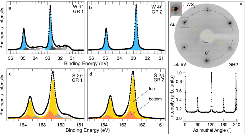
High-resolution W core-level spectra measured after GR1 and GR2 are shown in Figure 1a and b, respectively. For GR1, the main spin-orbit doublet, interpreted as stemming from SL WS2 (blue component)Dendzik et al. (2015b), is accompanied by many small contributions (grey components) at lower binding energy (BE), attributed to incompletely sulfided W species of the form \ceWS_2-x or metallic W clusters, as observed earlier for the same system Dendzik et al. (2015b); Shpak et al. (2010); Fuchtbauer et al. (2013). For GR2, on the other hand, these additional components are entirely absent and the W 4 spectrum shows a single peak at eV, characteristic of SL \ceWS2Dendzik et al. (2015b), with its spin-orbit doublet separated by 2.14 eV. The line-shape parameters used for the spectral deconvolution are given in Supplementary Material.
In Figure 1c and 1d we show the S spectra resulting from the two growth procedures. Two main components are visible in each of the spin-orbit peaks, indicated in light (S BE=162.45 eV) and dark (S BE=162.59 eV) orange: the latter has been assigned to S atoms from the ‘bottom’ (close to the Au(111) surface) while the former stems from the ‘top’ atoms in the S-W-S sandwich arrangement of \ceWS2. This interpretation follows the assignments for SL \ceMoS2 prepared on Au(111) Bana et al. (2018), and it will be discussed in the XPD experiments aiming to determine the polytype of the SL (see Supplementary Material). Besides these two components we observed several extra peaks at lower binding energy for GR1 , which are originating from species other than \ceWS2. On the contrary, the spectrum acquired on GR2 shows the spectral components associated with top and bottom sulfur only, indicating a better quality of the grown layer.
Figure 1e reports the LEED pattern acquired on the GR2 sample. The most intense spots corresponding to the reciprocal lattice of \ceWS2 are surrounded by moiré satellites, due to the lattice mismatch between \ceWS2 and the Au substrateDendzik et al. (2015b). The first order Au(111) diffraction spots also exhibit a hexagonal pattern, though slightly bigger in dimension due to a smaller lattice vector, and they are aligned with those of \ceWS2 (see dashed yellow line in Figure 1e and inset thereinto). By comparing the reciprocal lattice vectors of \ceWS2 with those of Au(111), we obtain a moiré periodicity of nm, in close agreement with literature Dendzik et al. (2015b). This is indicative of the formation of a superstructure with a periodicity of -\ceWS2 on -Au unit cell configuration.
Furthermore, the LEED pattern acquired on GR2 displays a three-fold symmetry (as evidenced by the circular profile taken across the \ceWS2 spots in the pattern), which could indicate the presence, for this sample, of a single azimuthal orientation of the \ceWS2 crystalline domains. However, a conclusive answer about the orientation of the layers and about the absence of detrimental mirror domains can only be obtained by means of XPD experiments.
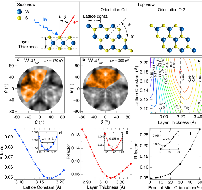
In XPD, photoemission intensity modulations arise from the interference between the component of the photoelectron wave field that reaches the detector directly from the emitting atom and the components scattered by atoms surrounding the emitter. This makes XPD very sensitive to the local environment of the emitter Woodruff (2007), hence making this technique ideal to address questions about the polytype of the layer (trigonal prismatic or octahedral), the distribution of mirror domains and other structural parameters such as lattice constant and layer thickness.
We acquired XPD patterns from the W core level on the layer produced with GR2 using a photon energy eV (photoelectron kinetic energy, KE137 eV), at which both forward and backward scattering contributions are significant, and at eV (KE326 eV), enhancing the forward scattering and suppressing the backscatteringWoodruff (2007). The experimental XPD patterns (color sector in Figure 2a and b) were compared to simulations (greyscale) using the reliability factor (R-factor) analysis (see Methods). Simulated diffraction patterns were calculated for different structural phases and their corresponding structural parameters assuming, as initial guess, the trigonal prismatic (1H) phase (sketched in Figure 2), following the indications obtained earlier for this system Dendzik et al. (2015b). The presence of two orientations in the SL can be modeled by assuming an incoherent superposition from the domains, such that the total photoemission intensity is
| (4) |
where is the contribution to the XPD pattern from the main orientation (Or1) and is the contribution from the mirror orientation (Or2), according to the models shown in top-right of Figure 2. The simulated XPD patterns for the two mirrored orientations stemming from W (KE326 eV) are reported in the Supplementary Material.
The three-fold symmetry of the simulated patterns for a single orientation matches the experimental data, which is a direct experimental indication of a dominant domain orientation and hints at a minor contribution from the mirror orientation. However, a conclusive determination of the layer orientation was achieved only through the R-factor analysis, as shown in the following. For the simulations of the photoemission intensity by multiple scattering calculations, the values for layer thickness (i.e. the vertical S-S distance), the lattice constant and the fraction of mirror domains in the SL, assuming the 1H phase, were changed independently, running an R-factor optimization in the three-dimensional parameter space, using the data sets of both Figure 2a and b. The analysis clearly reveals a global minimum for a single orientation structure (a maximum of 5% contribution of mirror domains), a lattice parameter of Å and a layer thickness of Å in very good agreement with the values reported in literature Schutte et al. (1987). The very low absolute value of the minimum R-factor () indicates an excellent agreement between experiment and simulation. For the sake of simplicity, Figure 2c reports a two-dimensional plot of the R-factor as a function of lattice constant and layer thickness obtained for the single orientation (). Figures 2d and 2e are obtained by taking cuts along the dashed lines in panel (c) to highlight the R-factor trend around the absolute minimum, while Figure 2f clearly shows that a minimum of R-factor is observed when only a single orientation is present. This is a considerably different from earlier reports on the growth of SL \ceWS2 by bottom-up approaches Fuchtbauer et al. (2013), in which the presence of detrimental mirror domains could not be avoided.
A similar analysis on the XPD patterns from S and W was performed assuming a octahedral (1T) polytype for the \ceWS2 SL. The simulations of the XPD patterns were performed using the same lattice constant and layer thickness determined earlier for the 1H polytype. The analysis returned higher values of the R-factor for the 1T phase, ruling then out this structure. The details of this analysis are reported in the Supplementary Material.
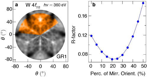
To understand whether also GR1 leads to a singly-oriented SL \ceWS2, we carried out an R-factor analysis simulating XPD patterns with a different percentage of mirror domains and compared them with the experimental pattern obtained from the W peak belonging to \ceWS2 acquired on GR1 (Figure 3a). The other structural parameters, obtained from the analysis on GR2, remained unchanged. In this case, the absolute minimum of the R-factor (0.07) was found when including 20% of mirror domains in the simulation, as shown in Figure 3b.
It is interesting to ask what physical mechanisms are responsible for the growth of the single orientation. The only element breaking the symmetry is the Au(111) substrate. While the first Au layer has a six-fold symmetry, considering deeper layers lowers the symmetry to three-fold, providing a suitable template for the growth of singly-oriented \ceWS2. However, this feature can only be exploited by an adequate choice of the growth parameters, in particular the W deposition rate, the substrate temperature and the \ceH2S partial pressure. Optimizing these does not only improve the quality of the resulting SL \ceWS2 but drives the formation of a single domain orientation. This could be favorable to achieve in GR2 because a higher temperature allows an enhanced surface diffusion of W atoms on the Au substrate while a lower W deposition rate, together with a higher \ceH2S background pressure, avoids the formation of partially sulfided species, as seen by XPS.
Having established that GR2 results in the growth of a single domain orientation, we used the XPD pattern from the W core-level component for GR2 to determine the orientation of the \ceWS2 layer with respect to the Au(111) substrate. In order to do this, we determined the orientation of the Au(111) substrate by measuring an XPD pattern stemming from the bulk component of Au on the clean Au sample, i.e. before the deposition of \ceWS2.
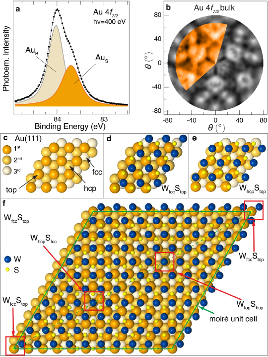
Figure 4a shows the typical Au spectrum acquired on clean Au(111). This is part of the series used to determine the XPD pattern of the bulk component AuB, which is shown (colored sector) in Figure 4b together with a simulated XPD pattern (grey sector) obtained using a 4 layer slab, bulk terminated Au(111) surface, with emitters in the second and deeper layers. A good agreement of the three fold symmetric pattern (corresponding to the (111) crystal stacking) with the simulation (R-factor=0.2), returns the orientation of the Au crystal as given in Figure 4c. Details about this R-factor analysis are given in Supplementary Material. Figure 4d and 4e show the two possible orientations of the SL \ceWS2 on Au(111). We call these configurations \ceW_fccS_top and \ceW_hcpS_top, in analogy with the case of h-BN on Ir(111)Orlando et al. (2014). In the former configuration the sulfur atoms at the left bottom corner are adsorbed in atop position and the W atoms adsorb in the fcc hollow sites, while in the latter W sits in hcp hollow sites. The comparison between the XPD patterns of the Au substrate and of the \ceWS2 overlayer unambiguously proves that the singly-oriented \ceWS2 sample assumes the configuration \ceW_fccS_top shown in Figure 4d. In Figure 4e we show a sketch of the entire moiré unit cell consisting of the \ceWS2 superstructure on the Au unit cell for the \ceW_fccS_top orientation. For the mixed domain growth produced with GR1, only 80% of domains are oriented with the \ceW_fccS_top configuration, while the remaining 20% adopts the \ceW_hcpS_top orientation.
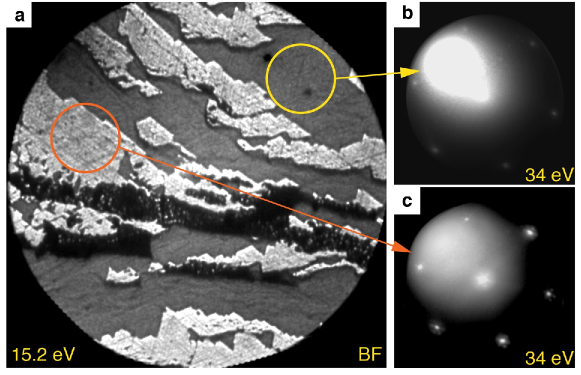
Details about the surface morphology and the size of the crystalline domains have been obtained from LEEM measurements, carried out on a SL \ceWS2 sample prepared ex-situ according to the GR2 procedure. In Figure 5a, a typical LEEM image of the surface is shown, acquired using the specular (00) LEED beam. This imaging condition is known as bright-field (BF) mode. The surface presents a distinct contrast, distinguishing bright and dark areas. Micro-LEED patterns recorded from a 1 micron large dark area show the diffraction pattern expected for bare Au substrate (yellow circle, Figure 5b) whereas the brighter areas are \ceWS2-covered regions (orange circle, Figure 5c) with the characteristic moiré, as seen in the large area LEED pattern in Figure 1e. The black areas in the center of the image can be related to surface contaminations due to transfer through air of the sample. Surface steps of the Au(111) substrate are also visible at these imaging conditions. It appears that \ceWS2 domains have grown on individual terraces and they stretch over several microns along the steps.
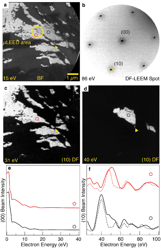
Figure 6a displays a BF image acquired at larger magnification. Again, the bright areas exhibit a LEED pattern with the moiré of \ceWS2 on Au(111) (Figure 6b). The use of a higher order LEED beam for imaging (dark-field imaging, DF), in this case the (10) beam, should allow for contrast between rotational domains of \ceWS2, given the three-fold symmetry of the LEED pattern at some energies, as already shown in the LEED pattern in Figure 1e. A DF image of the same surface area is presented in Figure 6c. The majority of the \ceWS2 domains show up bright at the chosen electron energy of 31 eV. Tuning the energy to 40 eV highlights other \ceWS2 islands, as can be seen in Figure 6d. We now show that the islands of different contrast correspond to opposite domain orientations. The dependence of the local LEEM intensity vs electron energy (so-called LEEM Flege and Krasovskii (2014)) at the points marked in red and black in figures 6c and 6d can be used to determine the local structureFlege et al. (2015). First, the curves of the (00) LEED beam for the two domains are compared in Figure 6e, revealing almost no difference. This finding directly proves that the two \ceWS2 domains have virtually the same atomic structure Flege and Krasovskii (2014); Flege et al. (2015). By contrast, the two curves obtained for the (10) spot, i.e. for the DF-mode image (filled lines in Figure 6f), are indeed dissimilar for the two different domains. While at 40 eV one \ceWS2 domain shows intense back reflection, at 31 eV the same domain reflects only weakly while the other does more strongly.
In order to confirm the structural origin of these differences, we show calculated curves (dashed lines in Figure 6f) for the two possible adsorption configurations of SL \ceWS2. A very good agreement between the experimental and calculated curves is found assigning the configuration \ceW_fccS_top to the majority of \ceWS2 domains (red) , while only a minor fraction of domains assumes the \ceW_hcpS_top (black). This interpretation is confirmed by LEED patterns acquired in each of the two regions (see Supplementary Material). Thus, the different domain orientations can be spotted at the nanoscale because of their different -curve fingerprint. From an overall quantitative evaluation of the available DF images, we derive a fraction of less than 5% of the surface being covered by the minority domains, in agreement with the results of the R-factor analysis performed for the XPD experiments. Moreover, these mirror domains are not uniformly distributed on the surface but rather were only found near surface defects, such as scratches or contaminations. This outcome sets the LEEM as an ideal technique to investigate the growth and features of TMDCs at the nanoscale, helping to understand the role of the deposition parameters and the growth mechanism from a microscopic point of view.
IV Conclusion
In summary, we have reported the characterization of the growth and structural features of \ceWS2 single layers on Au(111). We found that a low W deposition rate, a high partial pressure of \ceH2S and a high substrate temperature during the growth yield a unique crystalline orientation of SL \ceWS2, i.e. suppressing the presence of any detrimental mirror domains. Moreover, we have determined the layer stacking of \ceWS2 on the Au(111) substrate and obtained information about the morphology and size of the domains, highlighting the differences due to the growth conditions in the structure of the final layer.
Earlier studies about the growth of epitaxial SL \ceWS2 did rarely explore in quantitative detail the domain morphology and orientation. However, there have been indications of a domain mixture different from 50% for WS2 on Ag(111), as circular dichroism in the excitation of a valley polarization was observed for this system Ulstrup et al. (2017). We envision that the layers that we have grown and characterized in this work, combined with methods already available to transfer \ceWS2 from Au to other substratesGao et al. (2015), can be successfully employed in valleytronics and spintronics devices and applications.
Acknowledgements.
This work was supported by the Danish Council for Independent Research, Natural Sciences under the Sapere Aude program (Grant No. DFF-4002-00029) and by VILLUM FONDEN via the Centre of Excellence for Dirac Materials (Grant No. 11744). We thank Jan Lachnitt for fruitful discussion about the LEED- calculations and assistance with the AQuaLEED software package.References
- Novoselov et al. (2004) K. S. Novoselov, A. K. Geim, S. V. Morozov, D. Jiang, Y. Zhang, S. V. Dubonos, I. V. Grigorieva, and A. A. Firsov, “Electric field effect in atomically thin carbon films,” Science 306, 666–669 (2004).
- Novoselov et al. (2005a) K. S. Novoselov, A. K. Geim, S. V. Morozov, D. Jiang, M. I. Katsnelson, I. V. Grigorieva, S. V. Dubonos, and A. A. Firsov, “Two-dimensional gas of massless Dirac fermions in graphene,” Nature 438, 197–200 (2005a).
- Zhang et al. (2005) Y. B. Zhang, Y. W. Tan, H. L. Stormer, and P. Kim, “Experimental observation of the quantum Hall effect and Berry’s phase in graphene,” Nature 438, 201–204 (2005).
- Novoselov et al. (2005b) K. S. Novoselov, D. Jiang, F. Schedin, T. J. Booth, V. V. Khotkevich, S. V. Morozov, and A. K. Geim, “Two-dimensional atomic crystals,” Proceedings of the National Academy of Sciences of the United States of America 102, 10451–10453 (2005b).
- Splendiani et al. (2010) Andrea Splendiani, Liang Sun, Yuanbo Zhang, Tianshu Li, Jonghwan Kim, Chi-Yung Chim, Giulia Galli, and Feng Wang, “Emerging photoluminescence in monolayer MoS2,” Nano Letters, Nano Letters 10, 1271–1275 (2010).
- Mak et al. (2010) Kin Fai Mak, Changgu Lee, James Hone, Jie Shan, and Tony F. Heinz, “Atomically thin MoS2: A new direct-gap semiconductor,” Phys. Rev. Lett. 105, 136805 (2010).
- Radisavljevic et al. (2011) B. Radisavljevic, A. Radenovic, J. Brivio, V. Giacometti, and A. Kis, “Single-layer MoS2 transistors,” Nature Nanotechnology 6, 147 (2011).
- Lopez-Sanchez et al. (2013) Oriol Lopez-Sanchez, Dominik Lembke, Metin Kayci, Aleksandra Radenovic, and Andras Kis, “Ultrasensitive photodetectors based on monolayer \ceMoS2,” Nature Nanotechnology 8, 497–501 (2013).
- Xiao et al. (2012) Di Xiao, Gui-Bin Liu, Wanxiang Feng, Xiaodong Xu, and Wang Yao, “Coupled spin and valley physics in monolayers of MoS2 and other group-VI dichalcogenides,” Phys. Rev. Lett. 108, 196802 (2012).
- Mak et al. (2012) Kin Fai Mak, Keliang He, Jie Shan, and Tony F. Heinz, “Control of valley polarization in monolayer MoS2 by optical helicity,” Nature Nanotechnology 7, 494–498 (2012).
- Zeng et al. (2012) Hualing Zeng, Junfeng Dai, Wang Yao, Di Xiao, and Xiaodong Cui, “Valley polarization in MoS2 monolayers by optical pumping,” Nature Nanotechnology 7, 490–493 (2012).
- Cao et al. (2012) Ting Cao, Gang Wang, Wenpeng Han, Huiqi Ye, Chuanrui Zhu, Junren Shi, Qian Niu, Pingheng Tan, Enge Wang, Baoli Liu, and Ji Feng, “Valley-selective circular dichroism of monolayer molybdenum disulphide,” Nature Communications 3, 887 (2012).
- Mak et al. (2014) K. F. Mak, K. L. McGill, J. Park, and P. L. McEuen, “The valley hall effect in MoS2 transistors,” Science 344, 1489–1492 (2014).
- Xu et al. (2014) Xiaodong Xu, Wang Yao, Di Xiao, and Tony F. Heinz, “Spin and pseudospins in layered transition metal dichalcogenides,” Nature Physics 10, 343–350 (2014).
- Lee et al. (2012) Yi-Hsien Lee, Xin-Quan Zhang, Wenjing Zhang, Mu-Tung Chang, Cheng-Te Lin, Kai-Di Chang, Ya-Chu Yu, Jacob Tse-Wei Wang, Chia-Seng Chang, Lain-Jong Li, and Tsung-Wu Lin, “Synthesis of large-area MoS2 atomic layers with chemical vapor deposition,” Advanced Materials 24, 2320–2325 (2012).
- Shi et al. (2012) Yumeng Shi, Wu Zhou, Ang-Yu Lu, Wenjing Fang, Yi-Hsien Lee, Allen Long Hsu, Soo Min Kim, Ki Kang Kim, Hui Ying Yang, Lain-Jong Li, Juan-Carlos Idrobo, and Jing Kong, “van der waals epitaxy of MoS2 layers using graphene as growth templates,” Nano Letters, Nano Letters 12, 2784–2791 (2012).
- Li et al. (2015) Ming-Yang Li, Yumeng Shi, Chia-Chin Cheng, Li-Syuan Lu, Yung-Chang Lin, Hao-Lin Tang, Meng-Lin Tsai, Chih-Wei Chu, Kung-Hwa Wei, Jr-Hau He, Wen-Hao Chang, Kazu Suenaga, and Lain-Jong Li, “Epitaxial growth of a monolayer WSe2-MoS2 lateral p-n junction with an atomically sharp interface,” Science 349, 524–528 (2015).
- Pyeon et al. (2016) Jung Joon Pyeon, Soo Hyun Kim, Doo Seok Jeong, Seung-Hyub Baek, Chong-Yun Kang, Jin-Sang Kim, and Seong Keun Kim, “Wafer-scale growth of MoS 2 thin films by atomic layer deposition,” Nanoscale 8, 10792–10798 (2016).
- Lehtinen et al. (2015) Ossi Lehtinen, Hannu-Pekka Komsa, Artem Pulkin, Michael Brian Whitwick, Ming-Wei Chen, Tibor Lehnert, Michael J. Mohn, Oleg V. Yazyev, Andras Kis, Ute Kaiser, and Arkady V. Krasheninnikov, “Atomic scale microstructure and properties of Se-deficient two-dimensional MoSe2,” ACS Nano 9, 3274–3283 (2015).
- Chen et al. (2016) Xiang Chen, Yong Ju Park, Tanmoy Das, Houk Jang, Jae-Bok Lee, and Jong-Hyun Ahn, “Lithography-free plasma-induced patterned growth of MoS2 and its heterojunction with graphene,” Nanoscale 8, 15181–15188 (2016).
- Fu et al. (2017) Deyi Fu, Xiaoxu Zhao, Yu-Yang Zhang, Linjun Li, Hai Xu, A-Rang Jang, Seong In Yoon, Peng Song, Sock Mui Poh, Tianhua Ren, Zijing Ding, Wei Fu, Tae Joo Shin, Hyeon Suk Shin, Sokrates T. Pantelides, Wu Zhou, and Kian Ping Loh, “Molecular beam epitaxy of highly crystalline monolayer molybdenum disulfide on hexagonal boron nitride,” Journal of the American Chemical Society 139, 9392–9400 (2017).
- Kang et al. (2018) Won Tae Kang, Il Min Lee, Seok Joon Yun, Young Il Song, Kunnyun Kim, Do-Hwan Kim, Yong Seon Shin, Kiyoung Lee, Jinseong Heo, Young-Min Kim, Young Hee Lee, and Woo Jong Yu, “Direct growth of doping controlled monolayer WSe2 by selenium-phosphorus substitution,” Nanoscale 11, 566 (2018).
- Rycerz et al. (2007) A. Rycerz, J. Tworzydlo, and C. W. J. Beenakker, “Valley filter and valley valve in graphene,” Nature Physics 3, 172–175 (2007).
- Bana et al. (2018) Harsh Bana, Elisabetta Travaglia, Luca Bignardi, Paolo Lacovig, Charlotte E Sanders, Maciej Dendzik, Matteo Michiardi, Marco Bianchi, Daniel Lizzit, Francesco Presel, Dario De Angelis, Nicoleta Apostol, Pranab Kumar Das, Jun Fujii, Ivana Vobornik, Rosanna Larciprete, Alessandro Baraldi, Philip Hofmann, and Silvano Lizzit, “Epitaxial growth of single-orientation high-quality \ceMoS2 monolayers,” 2D Materials 5, 035012 (2018).
- Mak and Shan (2016) Kin Fai Mak and Jie Shan, “Photonics and optoelectronics of 2D semiconductor transition metal dichalcogenides,” Nature Photonics 10, 216–226 (2016).
- Orlando et al. (2014) Fabrizio Orlando, Paolo Lacovig, Luca Omiciuolo, Nicoleta G. Apostol, Rosanna Larciprete, Alessandro Baraldi, and Silvano Lizzit, “Epitaxial growth of a single-domain hexagonal boron nitride monolayer,” ACS Nano 8, 12063–12070 (2014).
- Zhu et al. (2011) Z Y Zhu, Y C Cheng, and U Schwingenschlögl, “Giant spin-orbit-induced spin splitting in two-dimensional transition-metal dichalcogenide semiconductors,” Physical Review B 84, 153402 (2011).
- Wang et al. (2012) Qing Hua Wang, Kourosh Kalantar-Zadeh, Andras Kis, Jonathan N Coleman, and Michael S Strano, “Electronics and optoelectronics of two-dimensional transition metal dichalcogenides,” Nature Nanotechnology 7, 699–712 (2012).
- Kormányos et al. (2015) Andor Kormányos, Guido Burkard, Martin Gmitra, Jaroslav Fabian, Viktor Zólyomi, Neil D Drummond, and Vladimir Fal’ko, “kp theory for two-dimensional transition metal dichalcogenide semiconductors,” 2D Materials 2, 022001 (2015).
- Baraldi et al. (2003) Alessandro Baraldi, Giovanni Comelli, Silvano Lizzit, Maya Kiskinova, and Giorgio Paolucci, “Real-time x-ray photoelectron spectroscopy of surface reactions,” Surface Science Reports 49, 169 – 224 (2003).
- García de Abajo et al. (2001) F. J. García de Abajo, M. A. Van Hove, and C. S. Fadley, “Multiple scattering of electrons in solids and molecules: A cluster-model approach,” Phys. Rev. B 63, 075404 (2001).
- Grønborg et al. (2015) Signe S. Grønborg, Søren Ulstrup, Marco Bianchi, Maciej Dendzik, Charlotte E. Sanders, Jeppe V. Lauritsen, Philip Hofmann, and Jill A. Miwa, “Synthesis of epitaxial single-layer MoS2 on Au(111),” Langmuir 31, 9700–9706 (2015).
- Dendzik et al. (2015a) Maciej Dendzik, Matteo Michiardi, Charlotte Sanders, Marco Bianchi, Jill A. Miwa, Signe S. Grønborg, Jeppe V. Lauritsen, Albert Bruix, Bjørk Hammer, and Philip Hofmann, “Growth and electronic structure of epitaxial single-layer WS2 on au(111),” Phys. Rev. B 92, 245442 (2015a).
- Woodruff (2007) D. P. Woodruff, “Adsorbate structure determination using photoelectron diffraction: Methods and applications,” Surface Science Reports 62, 1–38 (2007).
- Pendry (1980) J. B. Pendry, “Reliability factors for LEED calculations,” Journal of Physics C: Solid State Physics 13, 937–944 (1980).
- Flege et al. (2012) Jan Ingo Flege, Wen-Xin Tang, and Michael S Altman, “Low-Energy Electron Microscopy,” in Characterization of Materials, edited by Elton N. Kaufmann (John Wiley & Sons, Inc., Hoboken, NJ, USA, 2012) pp. 1808–1827.
- Flege and Krasovskii (2014) Jan Ingo Flege and Eugene E. Krasovskii, “Intensity-voltage low-energy electron microscopy for functional materials characterization,” Physica Status Solidi - Rapid Research Letters 8, 463–477 (2014).
- Flege et al. (2015) Jan Ingo Flege, Benjamin Herd, Jan Goritzka, Herbert Over, Eugene E. Krasovskii, and Jens Falta, “Nanoscale origin of mesoscale roughening: Real-time tracking and identification of three distinct ruthenium oxide phases in ruthenium oxidation,” ACS Nano, ACS Nano 9, 8468–8473 (2015).
- (39) Jan Lachnitt, “Aqualeed [software],” Private Communication.
- (40) A. Barbieri and M. A. Van Hove, Private Communication.
- Materer (2001) Nicholas F. Materer, “Layer stacking implementation of tensor low energy electron diffraction,” Surface Science 491, 131 – 139 (2001).
- Dendzik et al. (2015b) Maciej Dendzik, Matteo Michiardi, Charlotte Sanders, Marco Bianchi, Jill A. Miwa, Signe S. Grønborg, Jeppe V. Lauritsen, Albert Bruix, Bjørk Hammer, and Philip Hofmann, “Growth and electronic structure of epitaxial single-layer WS2 on au(111),” Phys. Rev. B 92, 245442 (2015b).
- Shpak et al. (2010) A P Shpak, A M Korduban, L M Kulikov, T V Kryshchuk, N B Konig, and V O Kandyba, “XPS studies of the surface of nanocrystalline tungsten disulfide,” Journal of Electron Spectroscopy and Related Phenomena 181, 234–238 (2010).
- Fuchtbauer et al. (2013) Henrik G. Fuchtbauer, Anders K. Tuxen, Poul G. Moses, Henrik Topsoe, Flemming Besenbacher, and Jeppe V. Lauritsen, “Morphology and atomic-scale structure of single-layer \ceWS2 nanoclusters,” Phys. Chem. Chem. Phys. 15, 15971–15980 (2013).
- Schutte et al. (1987) W. J. Schutte, J. L. De Boer, and F. Jellinek, “Crystal structures of tungsten disulfide and diselenide,” Journal of Solid State Chemistry France 70, 207–209 (1987).
- Ulstrup et al. (2017) Søren Ulstrup, Antonija Grubišić Čabo, Deepnarayan Biswas, Jonathon M. Riley, Maciej Dendzik, Charlotte E. Sanders, Marco Bianchi, Cephise Cacho, Dan Matselyukh, Richard T. Chapman, Emma Springate, Phil D. C. King, Jill A. Miwa, and Philip Hofmann, “Spin and valley control of free carriers in single-layer ,” Phys. Rev. B 95, 041405 (2017).
- Gao et al. (2015) Yang Gao, Zhibo Liu, Dong-Ming Sun, Le Huang, Lai-Peng Ma, Li-Chang Yin, Teng Ma, Zhiyong Zhang, Xiu-Liang Ma, Lian-Mao Peng, Hui-Ming Cheng, and Wencai Ren, “Large-area synthesis of high-quality and uniform monolayer WS2 on reusable Au foils,” Nature Communications 6, 8569 (2015).