X-ray photoemission and resistivity studies of the Pd-covered Ce thin films
Abstract
We have fabricated Ce/Pd bilayers grown on the SiO2 substrate by magnetron sputtering under ultrahigh vacuum. Usage of palladium layer on top of the Ce film appears to prevent effectively the sample oxidation. The thickness of the cerium films is between and thick palladium overlayers are always used. We have performed X-ray photoelectron spectroscopy on the as-deposited films and electrical resistivity measurements and XRD characterization. XPS confirms a very good quality of the samples. The analysis of the Ce spectrum suggests that the states of Ce are on the border between the fluctuating valence and localization. The resistivity measurements reveal a competition of the Kondo scattering, semiconducting and metallic behaviors as well as the influence of the dimensional effect.
Keywords: thin films, Kondo effect, photoelectron spectroscopy, dimensional effects
1 Introduction
In recent years many research publications have been focused on the use of lanthanides [1, 2] as protective coatings. Rare earth elements, such as Y, Ce, La, and Hf are widely known to affect the growth mechanisms of different oxides. Many surface treatments, such as sol-gel [3], chemical conversion coating [4] and physical vapour deposition technique [5], based on the use of cerium and its compounds have been investigated due to their low toxicity [6]. Recently, Canovic et al. [2] reported on high-temperature oxidation behaviour of a commercial Fe-22Cr steel coated by 10 nm Ce, 640 nm Co, and 10 nm Ce/640 nm Co thin films. They found, that applying a 640 nm Co layer on top of the 10 nm Ce layer, effectively reduces Cr evaporation and slows down the rate of alloy oxidation. However, to date there are not many literature reports on properties of single Ce layer.
Cerium is an anomalous lanthanide exhibiting unstable occupancy, which can lead to a fluctuating valence state [7, 8, 9], Kondo interactions [10, 11] or a localized magnetic moment up to [12, 13, 14]. Such behaviors have been widely observed in many compounds and alloys [7, 8, 9, 10, 11, 13, 14, 15, 16, 17, 18, 19, 20]. On the other hand, the effect of dimensionality can develop transition between various structures of Ce [21], i.e. the fcc (enhanced Pauli paramagnet) and the CurieWeiss paramagnets dhcp and fcc with localized magnetic moments. The fabrication and characterization of pure Ce thin films is a challenge by the reason of its high reactivity favouring creation of the Ce oxides. Aoki [21] prepared the Ce/Ta multilayers with thick Ta cover layer to reduce the oxidation process. For they found that the Ce phase was stabilized at low temperatures, whereas for a magnetic Ce was observed. Moreover, a crystalline state was found for the former and amorphous for the latter case. In the present research we have performed X-ray photoelectron spectroscopy (XPS) on the as-deposited single Ce thin films and electrical resistivity measurements for Ce films covered with a Pd overlayer.
2 Experimental
The Ce thin films were prepared at room temperature using an ultra high vacuum (UHV) magnetron sputtering [22, 23, 24]. As a substrate we have used Si(100) wafers with an oxidized surface to prevent a silicide formation [25]. Therefore, we have applied a special heat treatment in UHV before deposition, in order to obtain the SiO2 surface layer [26]. The Pdlayer was deposited using a DC source. For preparation of the Ce layer the RF source was used. The thickness of the cerium films has been varied in the range . Typical sputtering conditions used in deposition of the cerium and palladium thin films are listed in Table 1.
The chemical composition and the cleanness of all layers were checked , immediately after deposition, transferring the samples to an UHV analysis chamber equipped with X-ray Photoelectron Spectroscopy (XPS), Auger Electron Spectroscopy (AES) and ion gun etching system [27, 28, 29]. The XPS spectra were measured at room temperature using a SPECS EA 10 PLUS energy spectrometer with of 1486.6 eV. All emission spectra were measured immediately after the sample transfer in vacuum of . The measurements were conducted following routine backing procedures of the analysis chamber, which made possible reaching a base vacuum of . Calibration of the spectra was performed according to Baer [30]. The peak of gold was situated at 84.0 eV and the Fermi level was located at . Details of the XPS measurements can be found in [27, 28, 29].
The structural properties have been verified by standard X-ray diffraction (XRD) using radiation. The surface microstructure and roughness have been studied by Atomic Force Microscopy (AFM) using tapping mode. The resistivity measurements as a function of temperature were performed on the Quantum Design Physical Property Measurement System (PPMS) in Poznań. The usual method has been used in the electrical measurements. All the Ce thin films prepared for the resistivity and XRD measurements before transfer from UHV to environmental conditions were covered by the Pd protective layer of about 10 and 20 nm, respectively.
-
Parameter Ce Pd Rest gas pressure Argon partial pressure Argon purity 99.9998 Target diameter 51.5 mm Target purity 99 Distance between 220 mm substrate and target Magnetron sputtering RF DC method Sputtering power 40 W 35 W Deposition rate nms2 nms2 Substrate temperature 295 K
3 Results
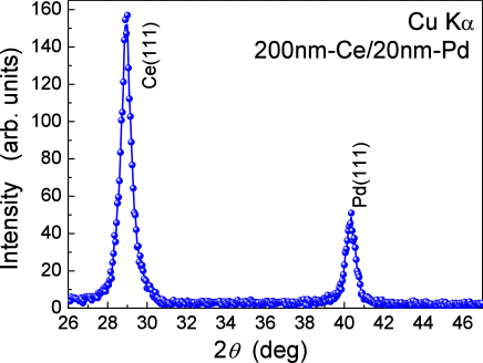
As indicated in previous section to verify the structure and morphology of the studied thin films characterization by XRD and AFM techniques has been performed. Figure 1 shows X-ray diffraction pattern for the sample measured at . The Bragg reflections are well resolved both for the positions expected for Ce and Pd sublayers. The peak position of Ce thin film is shifted relative to the position expected for bulk gama fcc cerium.
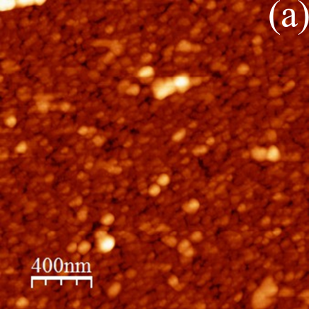
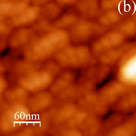
The exemplary surface morphology is illustrated in Figure 2 for the sample at RT. It results from Figure 2a that the surface is homogeneous and at the increased resolution used in Figure 2b it can be noticed that the grains are of the lateral dimensions of about . The estimated roughness parameters from the area 2000 nm 2000 nm (Figure 2a) were of about and , confirming a good quality of the films.
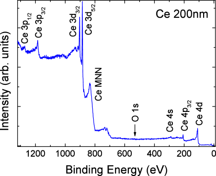
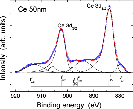
Further characterization of the films concerns the electronic properties, hence, the X-ray photoemission spectroscopy has been employed as it allows to verify the chemical purity of the material in respect to the nominal composition. The survey of the entire XPS spectra have shown neither the contamination of the oxygen nor carbon confirming a very high purity of the samples. A detailed identification of the main peaks in the binding energy range eV is presented in Figure 3. Due to well known high reactivity of cerium with oxygen we have prepared the thin film samples after an additional heating of the sample holder and the new substrate at for and cooling down to . It appeared that after such an outgassing procedure, it is possible to prepare oxygen and carbon free Ce surface. If the outgassing procedure is too short, the sample holder before deposition will not be perfectly clean. Moreover, if the XPS measurements were performed after a few hours delay the sample surface would already be partly oxidized despite the vacuum of in the analysis chamber. Then the intensity of the XPS signal decreases and the valence band can be artificially broadened. For our procedure the oxygen and other surface impurities are practically absent on the Ce thin films immediately after deposition. As can be seen in Figure 3, practically no XPS signal from potential contamination of atoms like O1s and C1s is observed.
The analysis of the Ce spectrum has been carried out in frames of the Gunnarsson and Schönhammer [8] and Fuggle [9] model. The Tougaard method was used to subtract the background. The experimental spectra were fitted using a mixture of Gaussian and Lorentzian shapes.
Apart from the main peaks Ce spectrum reveals satellites generated by the hybridization of the Ce states with the conduction electrons. The and final states satellites has intensity sensitive to the occupancy of the states, , and the hybridization energy, , respectively.
The intensity ratios:
| (1) | |||
| (2) |
enable determination of and from the theoretical and dependences [8, 9]. The decomposition presented in Figure 4 revealed a very small value of the hybridization energy and a slightly reduced occupancy of the states , which suggests that the states of Ce are on the border between a fluctuating valence and localized state.
In Figure 5 we have presented for the Ce(d)/Pd(10nm) bilayers with , and . The residual resistivity changes in the range , therefore in Figure 5 normalized results are shown to enable a comparison of different curves. It is evident that a competition of various contributions is responsible for the significant changes of the behavior while changing the Ce film thickness. We interpret the visible anomalies as resulting from the Kondo scattering due to the Kondo impurity effect within the Ce/Pd interface, the Crystalline Electric Field (CEF) effect at the upper range of the temperatures studied, and finally the dimensional effect appearing when the thickness of the bilayer becomes comparable with the scattering length. The behavior visible in Figure 5 leads to the conclusion that the dimensional effect switches on below .
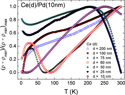
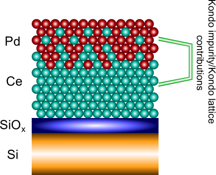
A detailed scenario can be proposed based on the illustration displayed in Figure 6. It is well known that the interface between Pd and Ce is relatively broad due to an interface mixing bulk Ce and Pd form Ce-Pd alloys [x] ([x] J.R. Thomson, J. Less Comon Metals 13 (1967) 307. In our case, this alloy formation is not homogenous and only near Pd-Ce interface takes place. Therefore, such an ultrathin layer could be not visable in XPS and XRD experiment. For thick Ce films a metallic resistivity dominates above , but at lower temperatures the dilution within Ce/Pd interface provides a Kondo and Kondo lattice contribution to the scattering, which results in the appearance of peaks at about implying a presence of correlations. These peaks are present as bumps for and and are better resolved below , when the contribution of metallic conductivity is reduced due to the size effect. For a semiconductor-like resistivity is observed at high temperatures and a high temperature peak develops at due to increasing metallic conductivity at lower temperatures. The low temperature peak ascribed previously to Kondo behavior switches to a minimum caused by the Kondo impurity mechanism. The last possibility is probable as, due to the ultrathin Ce film, there is a dropping amount of Ce ions within the interfaces and the ions start to behave like uncorrelated impurities.
4 Conclusion
A good quality Ce films covered with Pd overlayer have been fabricated, as confirmed by XRD and AFM studies of the structural properties and the morphology, respectively. The X-ray photoemission has shown that thick Pd layer effectively prevents the Ce film oxidation. The analysis of the Ce spectrum using the GunnarssonSchönhammerFuggle model indicates that the Ce states are on the border between the fluctuating valence and localization. A reasonable explanation of the temperature dependence of the resistance of the Ce films with thickness varied in the range is possible if one assumes importance of the mixing within the Ce/Pd interface. Then, depending on the Ce film thickness, Kondo or Kondo behavior can be concluded. At the upper range of the temperatures studied the Crystalline Electric Field influence is also possible. The dimensional effect expected when the thickness becomes comparable with the scattering length switches on below .
References
References
- [1] Ershov S, Druart M E, Poelman M, Cossement D, Snyders R and Olivier M G 2013 Corros. Sci. 75 158–168
- [2] Canovic S, Froitzheim J, Sachitanand R, Nikumaa M, Halvarsson M, Johansson L G and Svensson J E 2013 Surf. Coat. Technol. 215 62–74
- [3] Brusciotti F, Batan A, De Graeve I, Wenkin M, Biessemans M, Willem R, Reniers F, Pireaux J, Piens M, Vereecken J et al. 2010 Surf. Coat. Technol. 205 603–613
- [4] Campestrini P, Terryn H, Hovestad A and De Wit J 2004 Surf. Coat. Technol. 176 365–381
- [5] Dominguez-Crespo M A, Torres-Huerta A M, Rodil S, Brachetti-Sibaja S, De La Cruz W and Flores-Vela A 2010 J. Appl. Elektrochem. 40 639–651
- [6] Bethencourt M, Botana F, Calvino J, Marcos M and Rodriguez-Chacon M 1998 Corros. Sci. 40 1803–1819
- [7] Lawrence J, Riseborough P and Parks R 1981 Rep. Prog. Phys. 44 1
- [8] Gunnarsson O and Schönhammer K 1983 Phys. Rev. B 28 4315
- [9] Fuggle J, Hillebrecht F U, Zołnierek Z, Lässer R, Freiburg C, Gunnarsson O and Schönhammer K 1983 Phys. Rev. B 27 7330
- [10] Coqblin B, Arispe J, Bhattacharjee A and Evans S 1993 Kondo effect and heavy fermions Frontiers in Solid State Sciences, Selected Topics in Magnetism vol 2 ed Gupta L C and Multani M S (Singapore: World Scientific) p 75
- [11] Hewson A C 1997 Cambridge Studies in Magnetism vol 2 The Kondo problem to heavy fermions (Cambridge: Cambridge University Press)
- [12] Buschow K H J 1993 Handbook of magnetic materials vol 7 (Amsterdam: Elsevier North Holland)
- [13] Thalmeier P and Zwicknagl G 2004 Unconventional Superconductivity and Magnetism in Lanthanide and Actinide Intermetallic Compounds Handbook on the physics and chemistry of rare earths vol 34 ed Gschneidner K A, Bünzli J C G and Pecharsky V K (Amsterdam: Elsevier North Holland)
- [14] Maple M B 2005 J. Phys. Soc. Jpn. 74 222–238
- [15] Strydom A, Paschen S and Steglich F 2006 Physica B 378 793–794
- [16] Bauer E, Christianson A, Lawrence J, Goremychkin E, Moreno N, Curro N, Trouw F, Sarrao J, Thompson J, McQueeney R et al. 2004 J. Appl. Phys. 95 7201–7203
- [17] Synoradzki K and Toliński T 2016 Mater. Chem. Phys. 177 242–249
- [18] Toliński T 2007 Mod. Phys. Lett. B 21 431–454
- [19] Toliński T, Pugaczowa-Michalska M, Chełkowska G, Szlaferek A and Kowalczyk A 2002 Phys. Status Solidi B 231 446–450
- [20] Toliński T, Zlatić V and Kowalczyk A 2010 J. Alloy. Compd. 490 15–18
- [21] Aoki Y, Sato H, Komaba Y, Kobayashi Y, Sugawara H, Hashimoto S, Yokoyama T and Hanyu T 1996 Phys. Rev. B 54 12172
- [22] Smardz L 2005 J. Alloy. Compd. 395 17–22
- [23] Smardz L, Smardz K and Niedoba H 2000 J. Magn. Magn. Mater. 220 175–182
- [24] Smardz L 2002 J. Magn. Magn. Mater. 240 273–276
- [25] Skoryna J, Wachowiak M, Marczyńska A, Rogowska A, Koczorowski W, Czajka R and Smardz L 2016 Surf. Coat. Technol. 303 119–124
- [26] Smardz L, Köbler U and Zinn W 1992 J. Appl. Phys. 71 5199–5204
- [27] Smardz L, Nowak M and Jurczyk M 2012 Int. J. Hydrogen Energ. 37 3659–3664
- [28] Smardz K, Smardz L, Okonska I, Nowak M and Jurczyk M 2008 Int. J. Hydrogen Energ. 33 387–392
- [29] Skoryna J, Pacanowski S, Marczyńska A, Werwiński M, Rogowska A, Wachowiak M, Czajka R, Smardz L et al. 2016 Surf. Coat. Technol. 303 125–130
- [30] Baer Y, Busch G and Cohn P 1975 Rev. Sci. Instrum. 46 466–469