]www.ims.kit.edu ]www.ihfg.physik.uni-stuttgart.de
Fully on-chip single-photon Hanbury-Brown and Twiss experiment on a monolithic semiconductor-superconductor platform
Abstract
Photonic quantum technologies such as quantum cryptography Gisin et al. (2002), photonic quantum metrology Giovannetti et al. (2006); Dowling (2008); Müller et al. (2017), photonic quantum simulators and computers Kok et al. (2007); Ladd et al. (2010); Aspuru-Guzik and Walther (2012) will largely benefit from highly scalable and small footprint quantum photonic circuits. To perform fully on-chip quantum photonic operations, three basic building blocks are required: single-photon sources, photonic circuits and single-photon detectors Dietrich et al. (2016). Highly integrated quantum photonic chips on silicon and related platforms have been demonstrated incorporating only one Carolan et al. (2015) or two Wang et al. (2018) of these basic building blocks. Previous implementations of all three components were mainly limited by laser stray light, making temporal filtering necessary Reithmaier et al. (2015) or required complex manipulation to transfer all components onto one chip Khasminskaya et al. (2016). So far, a monolithic, simultaneous implementation of all elements demonstrating single-photon operation remains elusive. Here, we present a fully-integrated Hanbury-Brown and Twiss setup on a micron-sized footprint, consisting of a \BPChemGaAs waveguide embedding quantum dots as single-photon sources, a waveguide beamsplitter and two superconducting nanowire single-photon detectors. This enables a second-order correlation measurement at the single-photon level under both continuous-wave and pulsed resonant excitation.
Up to now, most quantum waveguide (WG) circuits have been fabricated from glass-based and Si-based materials. Both material platforms do not allow monolithic integration of deterministic single-photon sources. The used \BPChemInGaAs/\BPChemGaAs material system benefits from the capability of directly integrating on-demand non-classical light sources, namely semiconductor quantum dots (QDs) Michler et al. (2000). These emitters reach state-of-the-art performances in terms of single and indistinguishable photon emission, typically via a resonant excitation scheme Michler (editor). Within this platform, single-photon emission in combination with single-mode WGs and beamsplitters (BSs) was demonstrated with and without resonant excitation Prtljaga et al. (2014); Sapienza et al. (2010); Rengstl et al. (2015); Makhonin et al. (2014); Schwartz et al. (2016); Schnauber et al. (2018). Moreover, the implementation of superconducting nanowire single-photon detectors (SNSPDs) was successfully demonstrated on this material system Sprengers et al. (2011); Digeronimo et al. (2016); Reithmaier et al. (2015). These detectors represent the most suitable choice for working at the single photon level due to their potential near-unity detection efficiency ( Marsili et al. (2013)), low dark count rate and very high time resolution with intrinsic timing jitters in the ps range Sidorova et al. (2017); Korzh et al. (2018).
On the other hand, for silicon and silicon-related quantum photonic platforms a high degree of device complexity was reached, but efficient on-demand non-classical light sources are still missing Wang et al. (2018). By using parametric down conversion sources, only probabilistic single-photon emission is possible and the amount of stray light coming from the intense pump laser prevented so far the implementation of single-photon detectors on the same chip. Electrically-driven sources may solve this issue Khasminskaya et al. (2016); Bentham et al. (2016), but the used non-resonant excitation scheme typically leads to the emission of photons with a limited degree of indistinguishably that are less suitable for Hong-Ou-Mandel interference based operations. Another method attempted to overcome this limitation relies on the integration of optically active materials on silicon, but this hybrid approach significantly increases the fabrication complexity in comparison to a fully monolithic design Zadeh et al. (2016); Davanco et al. (2017); Murray et al. (2015); Ellis et al. (2018).
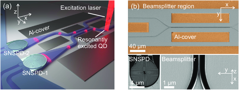
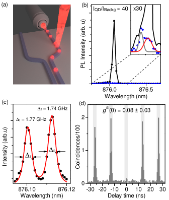
Here, a fully-\BPChemGaAs-integrated device is presented (Fig. 1(a)). For its characterization a standard cryogenic setup at with free-space access through optical windows is used. The QDs are embedded into a single-mode \BPChemGaAs ridge WG, where individual QDs can be optically excited with a resonant pump laser. The single-photon stream propagates across a 50:50 BS equipped with two independent SNSPDs at the output ports. In the present sample, the laser stray light is suppressed by means of metallic layers, deterministically placed to cover parts of the photonic chip. The utilized sample design allows for the comparison of the single-photon source performances both off- and on-chip. The QD emission propagating in the direction of the cleaved sample facet is collected with a microscope objective (Fig. 2(a)) and sent to an off-chip spectrometer or an off-chip Hanbury-Brown and Twiss setup.
The emission spectrum of the QD under pulsed resonant excitation (Fig. 2(b)) shows very low laser background propagating inside the WG: a ratio of 40:1 for QD emission-to-laser-background is observed. Under continuous wave (cw) excitation, the QD emission-to-stray-light ratio increases to 80:1, due to the smaller linewidth of the excitation laser compared to the linewidth used for pulsed excitation Schwartz et al. (2016). The investigated QD transition stems from an exciton (X) state with a fine structure splitting (FSS) of and linewidths of and , respectively (Fig. 2(c)). This is comparable to FSSs and linewidths of QDs in bulk material Richter et al. (2010), i.e. no degradation of the optical quality of the QD emission due to fabrication processes can be observed.
The off-chip Hanbury-Brown and Twiss experiment under pulsed resonant excitation shows nearly no coincidences at zero time delay, resulting in a of (Fig. 2(d)). The small non-vanishing part is caused by the low laser background inside the system and a possible re-excitation of the QD by the long excitation laser pulses Fischer et al. (2016) in almost equal proportion. In order to directly compare the device performances under off-chip and on-chip detection, no spectral filtering was used in the free-space experiment, since no light filtering is currently implemented on-chip.
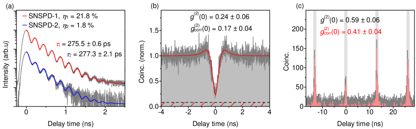
On-chip, the emission of the resonantly excited QD is guided to the coupling region of the on-chip BS, where it gets separated in the two WG arms and guided to the two SNSPDs. The measurements were done using the previously characterized QD. We reach detection efficiencies of up to for the first (SNSPD-1) and for the second SNSPD (SNSPD-2) close to their respective critical currents. During the measurements the bias current was set to approximately of the critical current to reduce the dark count rate. The associated detection efficiencies of the SNSPDs for these bias levels are and .
Time-correlated single-photon counting (TCSPC) experiments under resonant excitation were performed using both SNSPDs revealing a mono-exponential decay with superimposed distinct oscillations (Fig. 3(a)).
The decay time measured with SNSPD-1 (SNSPD-2) is () and the oscillation period (), respectively. This corresponds to () FSS of the QD X state. This is found in good agreement with the directly measured spectral detuning of the two fine structure components, which is (Fig. 2(c)). The depth of the oscillations is only limited by the instrument response function of our detection setup (approximately ). The WG acts as a polarization filter for QD emission with a polarization parallel to the WG since only the perpendicular in-plane polarization mode couples to the WG mode. These so-called quantum beats further prove the coherent nature of the used excitation method Flissikowski et al. (2001).
Correlating the two signals from the SNSPDs enables fully-integrated on-chip second-order correlation measurements. Under resonant cw excitation a distinct photon anti-bunching dip with a value of is found from the raw measurement data (Fig. 3(b)). This proves the functionality of a fully-integrated on-chip Hanbury-Brown and Twiss setup including all components in the same device. The laser stray light is strongly reduced, in comparison to previous state-of-the-art experiments, by covering the detector and the WG area with an \BPChemAlN/\BPChemAl bilayer. The deterministic alignment of the metallic layers shown here turned out to be of key importance for the reliability of the device. By subtracting dark counts, the value reduces to , which means that over of the detected photons are coming from QD emission. In order to use the QD as an on-demand source of single photons, we switched the excitation scheme to pulsed, still being in resonance with the X state.
A clear suppression of the zero-dealy peak is observed with a value of , when the dark counts of the detectors are subtracted (in comparison, a value of is found from raw data). With it can be seen that dominant signal stems from the single QD (), proving the full operation also under triggered excitation. The higher value in comparison to the one observed under cw excitation, is caused by the spectrally broader linewidth of the excitation laser and therefore an effectively lower signal-to-noise ratio Schwartz et al. (2016). Since the intensity of the QD emission drops when switching from cw to pulsed excitation, the relative dark count rate is also higher.
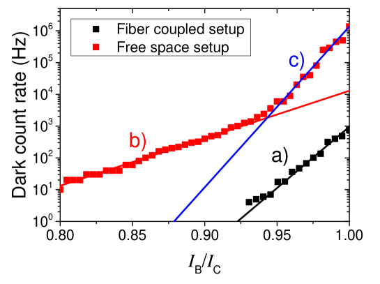
However, there is a significant scope to increase the signal-to-noise ratio by some obvious modifications of the photonic chip and the operation conditions. We anticipate a reduction of the stray light by further increasing the covered area and putting the Al-cover closer to the WGs. Detector dark counts can be reduced by decreasing the temperature of the used cryogenic setup Kitaygorsky et al. (2007). A further reduction of dark counts can be achived by properly shielding the detector from thermal photons. This can conveniently be done by the use of a fiber coupled instead of a free space setup. By placing an identically designed SNSPD in a fiber coupled setup, shielded in a metallic enclosure at , we were able to reduce the number of dark counts by over 2 orders of magnitude (see supplementary). Additionally, the signal level can be increased, e.g. by embedding the QDs into a WG resonator structure, and therefore increasing the coupling efficiency to the guided mode. Furthermore, the WG attenuation could be decreased by lowering the surface roughness through an improved etching process Rengstl et al. (2015) and a removal of the residual AlN-layer on top.
In conclusion, we successfully demonstrated a fully-integrated on-chip Hanbury-Brown and Twiss experiment, monolithically realized as a micron-sized \BPChemGaAs based device. The single photons emitted by a resonantly excited QD were guided and splitted in a single-mode waveguide BS and then detected on-chip with two \BPChemNbN superconducting nanowire single-photon detectors. A effective excitation laser stray light suppression using Al-covers allowed operation without any need of spectral filtering or time gating. The single-photon nature of the emission is clearly proven under cw and pulsed resonant excitation via the on-chip Hanbury-Brown and Twiss setup. For realizing large-scale quantum photonic chips with advanced functionality, additional elements such as phase shifters and multiple sources of indistinguishable single photons can be straightforward implemented on chip. Both components have already been successfully demonstrated on the InGaAs/GaAs platform. The first one even on-chip Dietrich et al. (2016) and the second one on the basis of wavelength-tunable individual devices Patel et al. (2010). The wavelength tuning can be enabled e.g. by strain or electric field tuning. The latter could be implemented by applying electrical contacts on both sides of the WGs to use the quantum-confined Stark effect for tuning the emission wavelength of the individual single-photon sources. Such measures together with the presented results pave the way for attractive on-chip quantum photonic applications such as tests of boson sampling, on-chip teleportation and photonic quantum computing.
I Methods
The chip was grown on a \BPChemGaAs (100) substrate using Metal-Organic Vapor-Phase Epitaxy (MOVPE) and is composed of a thick \BPChemAl_0.4Ga_0.6As confinement layer and a thick \BPChemGaAs core layer with implemented self-assembled \BPChemInGaAs/\BPChemGaAs QDs. The design of the sample without on-chip detectors can be found in Rengstl et al. (2015); Schwartz et al. (2016). The SNSPDs were structured on top out of a thick \BPChemNbN film with a critical temperature of . This value was determined as the temperature were the resistance drops to of the resistance before its superconducting transition. Between the \BPChemInGaAs layer and the \BPChemNbN, a thick \BPChemAlN-buffer layer was introduced to improve \BPChemNbN-film properties and therefore the sensitivity of our SNSPDs Schmidt et al. (2017). To decrease the effects of current crowding Clem and Berggren (2011), the SNSPD were shaped as an archimedean spiral in double spiral configuration (Fig. 1(a)) Henrich et al. (2013). The nanowires have a total length of and a width of with a gap of between the wires: further details on the fabrication of the nitride films and SNSPDs on \BPChemGaAs can be found in Schmidt et al. (2017). The WG, including the evanescent field coupler, were patterned on the detector chip using electron beam lithography with thick hydrogen silsesquioxane (HSQ) resist and an etching process performed via inductively coupled plasma reactive ion etching in Argon + \BPChemSiCl_4 atmosphere. After etching, the HSQ and the \BPChemAlN buffer layer remained on the WG. The WGs were patterned to a width of and etched to a depth of to support only the fundamental TE and TM mode. The 50:50 BS was designed as a directional WG coupler with a length of and a gap of . Since the detector has a diameter of , the WG was broadened using a linear taper over a distance of , beginning at a width of approximately to a final width of to embed the complete detector area (Fig. 1(b)). To decrease the effect of direct stray light from the exciting laser, the detectors were covered by of \BPChemAlN for isolation, followed by a thick reflecting \BPChemAl layer deposited by sputtering followed by lift-off. The same \BPChemAlN/\BPChemAl bilayer was added along the sides of the WG to decrease the amount of stray light scattered in the substrate (Fig. 1(b)).
After fabrication, the chip was cleaved perpendicularly to the WGs and placed into a liquid helium flow cryostat at a temperature of approximately . The used optical setup allows free-space access at the top and the side of the sample through quartz windows in the cryostat lid, focusing and collecting the light via microscope objectives. This enables the excitation of QDs from the top with a laser source and the simultaneous observation of light transmitted into both directions of the WG.
In one direction the emission of the QD propagates approximately in the straight WG, is coupled out and collected with a microscope objective. In the other direction, the light propagates to an evanescent field coupler, where it is separated into two distinct WG arms. Both arms are tapered at the end and are containing a SNSPD. The overall propagation distance from the QD to the SNSPDs is approximately . The absorption of our on-chip WG was characterized to be . This value is higher in comparison to state of the art WGs of our group, for which attenuation levels of were reached Rengstl et al. (2015). We assign this to a higher surface roughness of the WG sidewalls and absorption in the remaining \BPChemAlN buffer layer on top of the WG. Off-chip characterization of cw and pulsed resonant-excitation was performed with one QD in the WG at a wavelength of approximately . For cw resonant excitation, the spectral width of the excitation laser was . For pulsed resonant excitation the QD was excited starting with spectrally broad excitation pulses (FWHM ). These pulses were shaped in order to achieve a sufficiently small spectral linewidth, closer to the emission linewidth of the QD to further reduce the laser stray light in the system (temporal width , FWHM Schwartz et al. (2016). The polarisation of the excitation laser was chosen parallel to the WG and thereby tilted at around 45° towards the polarisation axes of the X state of the QD. To reduce charge fluctuations in the vicinity of the QD, an additional weak off-resonant laser ( power of the resonant laser) at wavelength of was used Nguyen et al. (2012).
For resonant cw excitation of the QD the overall count rate of SNSPD-1 (SNSPD-2) was (), the contribution of stray light counts from the excitation and stabilization laser was () and the share of dark counts was (). Therefore, the ratio between QD emission and noise in form of stray light and dark counts is 16:1 for SNSPD-1 and 3:1 for SNSPD-2. This leads to a theoretical value of which is in good agreement to the fitted value of . In comparison to measurements without \BPChemAl covers (not shown), the amount of straylight decreases by approximately a factor of .
The data that support the findings of this study are available from the corresponding author upon reasonable request.
Acknowledgements.
II Acknowledgments
The authors would like to thank T. Reindl and E. Reutter in the group of J. Weis from the Max Planck Institute for Solid State Research for electron beam lithography of the waveguide structures. This work was supported by the DFG project MI 500/29-1. The research of the IQST is financially supported by the Ministry of Science, Research and Arts Baden-Württemberg
III Figures and captions
References
- Gisin et al. (2002) N. Gisin, G. Ribordy, W. Tittel, and H. Zbinden, Rev. Mod. Phys. 74, 145 (2002).
- Giovannetti et al. (2006) V. Giovannetti, S. Lloyd, and L. Maccone, Phys. Rev. Lett. 96, 010401 (2006).
- Dowling (2008) J. P. Dowling, Contemporary Physics 49, 125 (2008).
- Müller et al. (2017) M. Müller, H. Vural, C. Schneider, A. Rastelli, O. G. Schmidt, S. Höfling, and P. Michler, Phys. Rev. Lett. 118, 257402 (2017).
- Kok et al. (2007) P. Kok, W. J. Munro, K. Nemoto, T. C. Ralph, J. P. Dowling, and G. J. Milburn, Rev. Mod. Phys. 79, 135 (2007).
- Ladd et al. (2010) T. D. Ladd, F. Jelezko, R. Laflamme, Y. Nakamura, C. Monroe, and J. L. O’Brien, Nature 464, 45 (2010).
- Aspuru-Guzik and Walther (2012) A. Aspuru-Guzik and P. Walther, Nature Physics 8, 285 (2012).
- Dietrich et al. (2016) C. P. Dietrich, A. Fiore, M. G. Thompson, M. Kamp, and S. Höfling, Laser & Photonics Reviews 10, 870 (2016).
- Carolan et al. (2015) J. Carolan, C. Harrold, C. Sparrow, E. Martín-López, N. J. Russell, J. W. Silverstone, P. J. Shadbolt, N. Matsuda, M. Oguma, M. Itoh, G. D. Marshall, M. G. Thompson, J. C. F. Matthews, T. Hashimoto, J. L. O’Brien, and A. Laing, Science 349, 711 (2015).
- Wang et al. (2018) J. Wang, S. Paesani, Y. Ding, R. Santagati, P. Skrzypczyk, A. Salavrakos, J. Tura, R. Augusiak, L. Mančinska, D. Bacco, D. Bonneau, J. W. Silverstone, Q. Gong, A. Acín, K. Rottwitt, L. K. Oxenløwe, J. L. O’Brien, A. Laing, and M. G. Thompson, Science (2018), 10.1126/science.aar7053.
- Reithmaier et al. (2015) G. Reithmaier, M. Kaniber, F. Flassig, S. Lichtmannecker, K. Müller, A. Andrejew, J. Vučković, R. Gross, and J. J. Finley, Nano Letters 15, 5208 (2015).
- Khasminskaya et al. (2016) S. Khasminskaya, F. Pyatkov, K. Słowik, S. Ferrari, O. Kahl, V. Kovalyuk, P. Rath, A. Vetter, F. Hennrich, M. M. Kappes, G. Gol’tsmann, A. Korneev, C. Rockstuhl, R. Krupke, and W. H. P. Pernice, Nature Photonics 10, 727 (2016).
- Michler et al. (2000) P. Michler, A. Kiraz, C. Becher, W. V. Schoenfeld, P. M. Petroff, L. Zhang, E. Hu, and A. Imamoglu, Science 290, 2282 (2000).
- Michler (editor) P. Michler (editor), Quantum Dots for Quantum Information Technologies (Springer, Berlin, 2017).
- Prtljaga et al. (2014) N. Prtljaga, R. Coles, J. O’Hara, B. Royall, E. Clarke, A. M. Fox, and M. S. Skolnick, Applied Physics Letters 104, 231107 (2014).
- Sapienza et al. (2010) L. Sapienza, H. Thyrrestrup, S. Stobbe, P. D. Garcia, S. Smolka, and P. Lodahl, Science 327, 1352 (2010).
- Rengstl et al. (2015) U. Rengstl, M. Schwartz, T. Herzog, F. Hargart, M. Paul, S. L. Portalupi, M. Jetter, and P. Michler, Applied Physics Letters 107, 021101 (2015).
- Makhonin et al. (2014) M. N. Makhonin, J. E. Dixon, R. J. Coles, B. Royall, I. J. Luxmoore, E. Clarke, M. Hugues, M. S. Skolnick, and A. M. Fox, Nano Letters 14, 6997 (2014).
- Schwartz et al. (2016) M. Schwartz, U. Rengstl, T. Herzog, M. Paul, J. Kettler, S. L. Portalupi, M. Jetter, and P. Michler, Opt. Express 24, 3089 (2016).
- Schnauber et al. (2018) P. Schnauber, J. Schall, S. Bounouar, T. Höhne, S.-I. Park, G.-H. Ryu, T. Heindel, S. Burger, J.-D. Song, S. Rodt, and S. Reitzenstein, Nano Letters 18, 2336 (2018).
- Sprengers et al. (2011) J. P. Sprengers, A. Gaggero, D. Sahin, S. Jahanmirinejad, G. Frucci, F. Mattioli, R. Leoni, J. Beetz, M. Lermer, M. Kamp, S. Höfling, R. Sanjines, and A. Fiore, Applied Physics Letters 99, 181110 (2011).
- Digeronimo et al. (2016) G. E. Digeronimo, M. Petruzzella, S. Birindelli, R. Gaudio, S. Fattah Poor, F. W. van Otten, and A. Fiore, in Photonics, Vol. 3 (Multidisciplinary Digital Publishing Institute, 2016) p. 55.
- Marsili et al. (2013) F. Marsili, V. B. Verma, J. A. Stern, S. Harrington, A. E. Lita, T. Gerrits, I. Vayshenker, B. Baek, M. D. Shaw, R. P. Mirin, and S. W. Nam, Nature Photonics 7, 210 (2013).
- Sidorova et al. (2017) M. Sidorova, A. Semenov, H.-W. Hübers, I. Charaev, A. Kuzmin, S. Doerner, and M. Siegel, Phys. Rev. B 96, 184504 (2017).
- Korzh et al. (2018) B. A. Korzh, Q. Y. Zhao, S. Frasca, J. P. Allmaras, T. M. Autry, E. A. Bersin, M. Colangelo, G. M. Crouch, A. E. Dane, T. Gerrits, F. Marsili, G. Moody, E. Ramirez, J. D. Rezac, M. J. Stevens, E. E. Wollman, D. Zhu, P. D. Hale, K. L. Silverman, R. P. Minin, S. W. Nam, M. D. Shaw, and K. K. Berggren, arXiv preprint arXiv:1804.06839 (2018).
- Bentham et al. (2016) C. Bentham, D. Hallett, N. Prtljaga, B. Royall, D. Vaitiekus, R. J. Coles, E. Clarke, A. M. Fox, M. S. Skolnick, I. E. Itskevich, and L. R. Wilson, Applied Physics Letters 109, 161101 (2016).
- Zadeh et al. (2016) I. E. Zadeh, A. W. Elshaari, K. D. Jöns, A. Fognini, D. Dalacu, P. J. Poole, M. E. Reimer, and V. Zwiller, Nano Letters 16, 2289 (2016).
- Davanco et al. (2017) M. Davanco, J. Liu, L. Sapienza, C.-Z. Zhang, J. V. M. Cardoso, V. Verma, R. Mirin, S. W. Nam, L. Liu, and K. Srinivasan, Nature communications 8, 889 (2017).
- Murray et al. (2015) E. Murray, D. J. P. Ellis, T. Meany, F. F. Floether, J. P. Lee, J. P. Griffiths, G. A. C. Jones, I. Farrer, D. A. Ritchie, A. J. Bennett, and A. J. Shields, Applied Physics Letters 107, 171108 (2015).
- Ellis et al. (2018) D. J. P. Ellis, A. J. Bennett, C. Dangel, J. P. Lee, J. P. Griffiths, T. A. Mitchell, T.-K. Paraiso, P. Spencer, D. A. Ritchie, and A. J. Shields, Applied Physics Letters 112, 211104 (2018).
- Richter et al. (2010) D. Richter, R. Hafenbrak, K. D. Jöns, W.-M. Schulz, M. Eichfelder, M. Heldmaier, R. Roßbach, M. Jetter, and P. Michler, Nanotechnology 21, 125606 (2010).
- Fischer et al. (2016) K. A. Fischer, K. Müller, K. G. Lagoudakis, and J. Vučković, New Journal of Physics 18, 113053 (2016).
- Flissikowski et al. (2001) T. Flissikowski, A. Hundt, M. Lowisch, M. Rabe, and F. Henneberger, Phys. Rev. Lett. 86, 3172 (2001).
- Kitaygorsky et al. (2007) J. Kitaygorsky, I. Komissarov, A. Jukna, D. Pan, O. Minaeva, N. Kaurova, A. Divochiy, A. Korneev, M. Tarkhov, B. Voronov, I. Milostnaya, G. Gol’tsman, and R. R. Sobolewski, IEEE Transactions on Applied Superconductivity 17, 275 (2007).
- Patel et al. (2010) R. B. Patel, A. J. Bennett, I. Farrer, C. A. Nicoll, D. A. Ritchie, and A. J. Shields, Nature Photonics 4, 632 (2010).
- Schmidt et al. (2017) E. Schmidt, K. Ilin, and M. Siegel, IEEE Transactions on Applied Superconductivity 27, 1 (2017).
- Clem and Berggren (2011) J. R. Clem and K. K. Berggren, Physical Review B 84, 174510 (2011).
- Henrich et al. (2013) D. Henrich, L. Rehm, S. Dörner, M. Hofherr, K. Il’in, A. Semenov, and M. Siegel, IEEE Transactions on Applied Superconductivity 23, 2200405 (2013).
- Nguyen et al. (2012) H. S. Nguyen, G. Sallen, C. Voisin, P. Roussignol, C. Diederichs, and G. Cassabois, Phys. Rev. Lett. 108, 057401 (2012).
IV Supplementary information to “Fully on-chip single-photon Hanbury-Brown and Twiss experiment on a monolithic semi-conductor-superconductor platform”
V SNSPD characterization
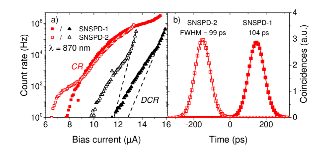
The SNSPDs were characterized at using laser emission at a wavelength of , centered between both SNSPDs (Fig. S1(a)). In this way, the SNSPDs can be characterized by utilizing stray light coming from the substrate, since the SNSPDs cannot be illuminated directly from top, due to the AlN/Al cover. SNSPD-1 has a critical current of and SNSPD-2 of . The critical current of SNSPD-2 is suppressed due to a long single constriction where the nanowire width is reduced to . The count rate dependencies of both SNSPDs coincide with each other for bias currents between and . For lower bias currents the effect of the constriction in the SNSPD-2 is observed. The higher current density of the nanowire at the constriction makes it sensitive for single photons at a bias current of and a strong increase in the count rate can be observed. At a bias current of the rest of the nanowire is starting to get sensitive for single photons and the full nanowire contributes to the measured count rate Zhang et al. (2014). To estimate the detection efficiency of the SNSPDs during the experiments, we used the integrated quantum dot under resonantly pulsed excitation. From the power dependent measurements shown in Fig. S2 we can extract an excited state preparation of . In combination with the repetition rate of the laser, the calculated coupling efficiency for QD emission to the WG () and the propagation losses over a distance of , a detection efficiency of for SNSPD-1 and for SNSPD-2 are calculated at the bias currents of and respectively. Taking into account the bias dependence of the detectors (Fig. S1(a)) we can calculate the efficiencies of our detectors to at a bias current of for SNSPD-1, the detection efficiency of SNSPD-2 is limited to at a bias current of , due to the constriction. The dark count rates (DCR) show clear signs of parasitic counts. When decreasing the bias currents below for SNSPD-1 and for SNSPD-2 respectively, it deviates from an exponential bias dependence, which would be expected for dark counts intrinsic to a SNSPD Yamashita et al. (2011). One of the reasons for this parasitic counts can be due to thermal radiation due to the open nature of our used free space cryostat. Furthermore, SNSPD-2 suffers from a high number of dark counts caused by the higher current density in the constriction. A comparison of DCRs between the used free space setup and a setup where an SNSPD with similar design was optically coupled with a fiber and placed in a metallic enclosure at , shows that in the latter case, the DCR can be reduced by over two orders of magnitude (see Fig. S3).
VI Instrumental response function
The instrumental response function () in Fig. S1(b) was measured for the full on-chip detection setup. (Eq.:1) is the for the correlation of a single SNSPD with the laser trigger, as used for TCSPC measurements. It is the convolution of the timing characteristics of the individual components in our setup: The timing variations of the corresponding electrical trigger signal , the timing jitter of the corresponding detector , caused by a the timing inaccuracy between absorption of the photon and occurrence of the detectors voltage pulse, the timing characteristic of the amplifiers and electronic cables , and the timing resolution of the used TCSPC electronic . A Gaussian fit reveals a full width half maximum (FWHM) value of for SNSPD-1 and for SNSPD-2 at a bias current of . Due to their very small pulse duration of approx. the influence of the unshaped excitation laser pulses are not taken into account.
(Eq.:2) is the for a correlation experiment using one SNSPD as start and the other as stop. It is the convolution of the excitation pulse duration , the timing accuracy of the corresponding detectors and , and the timing accuracy of the amplifiers and electronic cables as well as the used TCSPC electronic for each individual readout channel. We measured to be (FWHM).
| (1) | ||||
| (2) | ||||
VII Beam splitter
The used beamsplitter is an evanescent field coupler with a wavelength-dependent splitting ratio as depicted in Fig. S4. The measurements were done by exciting a QD ensemble in the WG with an excitation laser at . The photons from the quantum dot ensemble propagated to the beamsplitter and split into both output arms. The emission from the two output ports was collected with a microscope objective and sent to a spectrometer subsequently. Sharp emission lines representing individual quantum dots in the two recorded spectra were fitted with Gaussian functions and compared by their areas. With this method the splitting ratio of the investigated QD emission line of the main text can be given: (A splitting ratio of 0 would mean that no photons are coupled from the WG arm in which the QD is located to the other WG arm).
VIII Resonant excitation
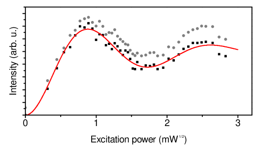
Excitation power dependent measurements of the QD intensity via pulsed resonant excitation revealed clear Rabi-oscillations which show the coherent excitation of the QD (Fig. S2). The data with subtracted laser background were fitted numerically by solving the optical Bloch equations of a two level system with a power dependent dephasing rate. A state preparation fidelity of is extracted from the fit.
For the fitting of the decay curves depiced in Fig. 3(a) of the main text, the product of an exponential decay and an harmonic oscillation
| (3) | ||||
is used Flissikowski et al. (2001). , , and are fit-parameters. The function is convolved with the instrumental response function, the pulse duration of the shaped excitation laser pulses () and combined with an additional Gaussian function to account for the effect of laser stray light in the system.
The second order correlation function in Fig. 3 (b) of the main text is fitted with the function
| (4) | ||||
The fit-function includes the effects of spectral diffusion caused by electrical fluctuation in the vicinity of the QD Rengstl et al. (2015) and coherent driven state oscillations Makhonin et al. (2014). The fit parameters and are the time-scale and the amount of the bunching which is caused by spectral diffusion. determines the amount of antibunching. is the radiative decay rate, the damping rate, C = and the Rabi-frequency. is assumed to be the reciprocal of the measured decay time from the excited state and can be calculated by excitation power-dependent measurements of the QD intensity, a measurement of the linewidth and the formulas Nguyen et al. (2012)
| (5) | ||||
is the intensity of the QD emission, is the power of the resonant laser and is the saturation-power of the QD emission. With and we can calculate , and . The remaining fit parameters are , and . By taking also into account the resolution of our measurement set up of by deconvoluting the data we achieve (If the detector resolution is not taken into account would be the result). As it can be seen in Fig. 3(b) of the main text the calculated function fits very good to the measurement data, including the width of the antibunching dip which is not fitted rather than calculated with and .

References
- Zhang et al. (2014) L. Zhang, L. You, D. Liu, W. Zhang, L. Zhang, X. Liu, J. Wu, Y. He, C. Lv, Z. Wang, and X. Xie, Aip Advances 4, 067114 (2014).
- Yamashita et al. (2011) T. Yamashita, S. Miki, K. Makise, W. Qiu, H. Terai, M. Fujiwara, M. Sasaki, and Z. Wang, Applied Physics Letters 99, 161105 (2011).
- Flissikowski et al. (2001) T. Flissikowski, A. Hundt, M. Lowisch, M. Rabe, and F. Henneberger, Phys. Rev. Lett. 86, 3172 (2001).
- Rengstl et al. (2015) U. Rengstl, M. Schwartz, T. Herzog, F. Hargart, M. Paul, S. Portalupi, M. Jetter, and P. Michler, Applied Physics Letters 107, 021101 (2015).
- Makhonin et al. (2014) M. N. Makhonin, J. E. Dixon, R. J. Coles, B. Royall, I. J. Luxmoore, E. Clarke, M. Hugues, M. S. Skolnick, and A. M. Fox, Nano Letters 14, 6997 (2014), pMID: 25381734.
- Nguyen et al. (2012) H. S. Nguyen, G. Sallen, C. Voisin, P. Roussignol, C. Diederichs, and G. Cassabois, Phys. Rev. Lett. 108, 057401 (2012).