Quantum Transport Properties of an Exciton Insulator/Superconductor Hybrid Junction
Abstract
We present a theoretical study of electronic transport in a hybrid junction consisting of an excitonic insulator sandwiched between a normal and a superconducting electrode. The normal region is described as a two-band semimetal and the superconducting lead as a two-band superconductor. In the excitonic insulator region, the coupling between carriers in the two bands leads to an excitonic condensate and a gap in the quasiparticle spectrum. We identify four different scattering processes at both interfaces. Two types of normal reflection, intra- and inter-band; and two different Andreev reflections, one retro-reflective within the same band and one specular-reflective between the two bands. We calculate the differential conductance of the structure and show the existence of a minimum at voltages of the order of the excitonic gap. Our findings are useful towards the detection of the excitonic condensate and provide a plausible explanation of recent transport experiments on HgTe quantum wells and InAs/GaSb bilayer systems.
Particles condensates are at the basis of superconductivity and superfluidity Leggett (2006, 2008). We can explain superconductivity in terms of condensation of Cooper pairs Bardeen et al. (1957). Similar processes of pairing and condensation can also take place in other systems. Mott postulated that semimetals (SMs) at sufficiently low temperatures could undergo a phase transition into an insulating state described by electron-hole bound pairs forming an exciton insulator (EI) Mott (1961). Interestingly, the EI phase can be described by a BCS-like theory Keldysh and Kopaev (1965); Jérome et al. (1967). The coupling strength of an EI is expected to be even weaker than the coupling in a conventional superconductor (S) and very fragile with respect to disorder Zittartz (1967). Additionally, excitons may recombine quite fast, thus not allowing to form a condensate easily. So far, the EI remains an elusive phase of matter since the original proposals Jérome et al. (1967); Zittartz (1967); Halperin and Rice (1968). To date, one of the most successful attempts to obtain a stable EI is based on the condensation of excitons coupled to light confined within a cavity — the so-called exciton-polaritons Kasprzak et al. (2006).
In order to reduce the electron-hole recombination rate it was suggested to use a system where electrons and holes are spatially separated. Examples of this are bilayer quantum well (QW) systems Lozovik and Yudson (1976); Shevchenko (1976), topological EIs Seradjeh et al. (2009); Pikulin and Hyart (2014); Budich et al. (2014), double two-dimensional electron gases in a strong magnetic field Macdonald and Rezayi (1990); Yoshioka and Macdonald (1990); Eisenstein and Macdonald (2004); Spielman et al. (2000); Kellogg et al. (2004); Tutuc et al. (2004), two parallel, independently gated graphene monolayers separated by a finite insulating barrier Lozovik and Sokolik (2008); Min et al. (2008); Kharitonov and Efetov (2008); Mak et al. (2011) and very recently two bilayer graphene electron system separated by hexagonal BN or WSe2 Li et al. (2016); Lee et al. (2016); Su and MacDonald (2017); Burg et al. (2018).
The fact that the flow of the EI condensate does not carry any charge current makes its detection rather difficult in bulk systems. Recent experiments suggested signatures of the EI phase in TiSe2 in the 1T phase Monney et al. (2010); Rossnagel (2011); Kogar et al. (2017). Also, metallic carbon nanotubes can be seen as SMs, thus are candidates to host an EI phase Varsano et al. (2017); Aspitarte et al. (2017); Senger et al. (2018). There are also investigations of Ta2NiSe5 as a host material for the EI phase Lu et al. (2017); Mor et al. (2017). However, results remain controversial.
In this article, we propose a way for the detection of an EI condensate by electrical measurements. Specifically, we focus on a setup consisting of an SM “sandwiched” between a normal and a superconductor electrode [see Fig. 1(a)], which is similar to the one explored in Refs. Kononov et al. (2016, 2017). These experiments showed the presence of a zero–bias anomaly in the differential resistance compatible with the size of the estimated EI gap of these systems. Both HgTe QWs and InAs/GaSb bilayer can be considered as SMs where the conduction band (CB) and the valence band (VB) have a finite energy overlap, but the relative minimum and maximum are displaced in the reciprocal space. Our results of the transport properties provide an interpretation of the experimental results and show that the zero-bias resistance can be associated with the existence of an EI condensate in the structure.
At a microscopic level the electronic transport through the structure shown in Fig. 1(a) result from the interplay between two channels of normal reflection and two channels of Andreev reflection. One of the normal reflection channels is the standard intra-band specular reflection, whereas the second one is an intra-band normal reflection directly associated to the presence of the EI region with a length of the order of the associated EI coherence length. This additional reflection dominates in the case that the length of the EI region exceeds the coherence length of the condensate. The presence of the superconductor gives also rise to two different Andreev reflections: a standard intra-band Andreev reflection that has a retro-reflective character as in standard S/N systems, and an inter-band Andreev specular reflection, similar to the Andreev specular-reflection in chiral SM Beenakker (2006). Contrary to the case of a chiral SM, the two channels of Andreev reflection can be open simultaneously, but the retro-reflective is usually dominating over the specular-one.
This Article is structured as follows: in Sec. I we present the model of a bulk EI coupled to a normal contact and to a superconductor contact; in Sec. II, we analyse the quantum transport properties of this hybrid junction and identify the reflection processes mentioned above. In Sec. III, we present results for the differential conductance of a two terminal system, and we contrast them with the experiments on differential resistance in Ref. Kononov et al. (2016, 2017).
I Model and Formalism
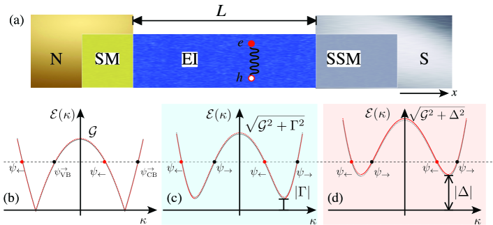
We consider a bulk SM, where we neglect the displacement in the reciprocal space between the minimum of the CB and the maximum of the VB Jérome et al. (1967); Rontani and Sham (2005a). The SM is contacted on the left with a normal metal and on the right with a superconductor. The two metallic contacts screen the Coulomb interaction in the regions close to them partially, thus, we can assume that Coulomb interaction is spatially modulated. In the unscreened region, we assume the formation of an EI characterised by a coupling strength of . Due to the proximity effect, a superconductive semi-metal (SSM) region is formed below the superconducting contact. An order parameter characterises the superconducting state.
In other words, the structure shown in Fig. 1(a) is modelled as a junction consisting of an SM electrode (), a central region of length with a finite EI coupling ( & ), and a SSM electrode with zero EI coupling and finite superconducting gap ( & ). Overall, we account for a finite overlap between the CB and VB. Formally, the hybrid junction is described by the following matrix Hamiltonian:
| (1) |
where is the standard momentum operator and the pairing functions are
| (2a) | |||||
| (2b) | |||||
and is the Heaviside step function. The Hamiltonian (1) is written in terms of the Pauli matrices in the band sub-space: CB and VB, and the Pauli matrices electron and hole (Nambu) subspace De Gennes (1999). As a consequence the Hamiltonian is written in the basis defined by the bi-spinor , Dolcini et al. (2010); Peotta et al. (2011); Bercioux et al. (2017). The order parameters and are assumed to be step-like functions in real space and no self-consistent calculation is carried out.
We account for possible elastic reflections at the hybrid interfaces, SM/EI and EI/SSM, by introducing two delta-like barriers in the Hamiltonian Eq. (1) Blonder et al. (1982); Rontani and Sham (2005a):
| (3) |
These reflections can be ascribed, for example, to the mismatch of the Fermi wave vector in the different regions. Within this model, we assumed a sharp boundary between the different regions and an abrupt change of the excitonic and superconducting pair correlations at the SM/EI interface and EI/SSM one, respectively. This assumption is well justified if the size of the contact between the two regions is much smaller than its lateral dimensions. This condition can be achieved experimentally by proper design of the contact. However, even in the case of a smooth transition of the pair correlations at the interface, we expect to have qualitatively similar results.
In the next three subsections, we introduce the scattering states necessary for evaluating the quantum transport properties of the hybrid junction. We assume incoming particles from the normal contact and determine the different scattering processes.
I.1 The semi-metal contact
For the scattering state in the SM contact on the left side, we assume that both the CB and the VB will contribute to the overall conductance — this is justified by the equal population of both bands at the Fermi energy Jérome et al. (1967) [c.f. Fig. 1(b)]. Therefore, an incoming scattering state from the CB reads:
| (4a) |
whereas an incoming scattering state from the VB will read:
| (4b) | |||||
In Eqs. (4) we identify four possible types of reflection: two normal reflections, where an electron is reflected as an electron either in the CB ( and ) or in the VB ( and ), and two Andreev-like reflections where an electron is converted in a hole either of the CB ( and ) or of the VB ( and ). In the two scattering states (4), is the longitudinal component of the momentum.
The two Andreev reflections are qualitatively different: whereas the Andreev reflection within the same band is a retro-reflection process, the inter-band Andreev process is a specular reflection, similarly to the one predicted in single- and bi-layer graphene Beenakker (2006); Ludwig (2007); Efetov et al. (2015), Weyl SM Chen et al. (2013) and three-dimensional topological insulators Breunig et al. (2018); Bercioux and Lucignano (2018). The main difference is that in our hybrid junction, the two Andreev processes take place at the same energy, whereas in chiral SMs either it is either a retro- or a specular-reflection process. Also, the two types of normal reflection have different propagation direction: normal reflection within the same band is specular whereas it is retro-reflective when the band is changed (see Fig. 2 for more details).
The scattering dynamics can be understood considering the conservation of the energy , and of the transversal momentum . We can express the longitudinal component of the momentum in terms of these two conserved quantities:
| (5) |
The injection of carriers from the VB (4b) is allowed only for energies smaller than the band overlap , than the VB closes and we are left with a single band system.
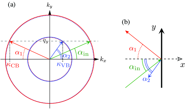
Using the same conservation considerations, we can obtain the various reflection angles (see Fig. 2):
| (6a) | ||||
| (6b) | ||||
| with . The moduli are expressed in terms of | ||||
| (6c) | ||||
The intra-band normal reflection band has a propagation direction opposite to the incoming one; the same is true for inter-band Andreev reflection electrons that are converted into holes of the opposite band: . For electrons injected from one band and converted into a hole of the same band (intra-band Andreev reflection), or into an electron of the other band (inter-band normal reflection), the reflection angle is:
| (7) |
When the injection energy exceeds the band overlap , the angle becomes complex and the corresponding mode is evanescent. By imposing we can determine the critical injection angle :
| (8) |
The intra-band Andreev reflection and the inter-band normal reflection are exactly retro-reflective only in the Andreev-limit of , whereas by construction, the inter-band Andreev specular-reflection and the intra-band normal reflection are always opposite to the injection angle (a sketch of the various angles is in Fig. 2). Furthermore, the inter-band Andreev reflection is a second-order process — it requires scattering at both interfaces and a finite transmission through the EI region.
I.2 The semi-metal superconducting contact
In the SSM region, the superconducting pairing couples electrons and holes of the same band, but we assume no inter-band coupling. An incoming particle from the SM region can be transmitted as quasi-electron or quasi-hole either in the CB ( and ) or in the VB ( and ). The transmitted wave function reads:
| (9) |
The longitudinal component of the momenta in the SSM region [c.f. Fig. 1(d)] are
| (10) |
The coherence factors, and , are the ones of a -wave superconductor. Note that coherent factors have opposite signs for the CB and VB, this is due to the different curvature of these two bands:
| (11a) | ||||
| (11b) | ||||
Importantly, we are assuming that the superconducting pairing is not pairing the CB and the VB; thus we are dealing with a two-band superconductor Zehetmayer (2013).
I.3 The excitonic insulator
In the middle region, there is a finite Coulomb pairing between electrons in the CB and the VB that leads to the excitonic insulator. Here, we can express the wave function as counter-propagating states for the four possible states:
| (12) |
II Transport properties of the hybrid junction
We evaluate the amplitudes of the various scattering processes by imposing the continuity of the wave functions at the two interfaces, :
| (15a) | ||||
| (15b) | ||||
Because of the delta-function potential (3) at the interfaces, the first derivative may exhibit a jump with a different sign for the CB and VB electrons Rontani and Sham (2005a, b). Specifically,
| (16a) | |||
| (16b) | |||
In order to simplify the discussion on the various scattering mechanisms, we consider the case of the injection of an electron from the CB, Eq. (I.1). For energies smaller than and , at the first interface between the SM and the EI, the incoming electron can be normal reflected in the same band or normal reflected in the valence band . The latter process is equivalent to the Andreev reflection at a normal metal-S interface Rontani and Sham (2005a, b); Wang et al. (2005); Bercioux et al. (2017) and leads to the formation of an exciton pair.
At the interface with the superconductor, a quasi-particle state of the EI condensate [a linear combination of CB and VB Eq. (I.3)] can be Andreev-reflected into a hole either in the same band — , or into the other band — .
For energies higher than the EI gap, , the quasi-particles travel through the EI region as propagating waves. On the contrary, for energy below the excitonic gap, the quasi-bound states are characterised by a complex momenta describing evanescent modes. The characteristic decay length of these modes is energy dependent and is given by:
| (17) |
where ; here is the momentum parallel to the interfaces that is conserved in the scattering process. When the band overlap is the dominant energy scale, i.e., — the Andreev limit Andreev (1964); Zagoskin (2014) — and therefore
| (18) |
In the following we focus on the sub-gap transport, i.e. we consider the injection of electrons from the SM contact with energies smaller than the superconducting gap, ; we further assume that .
When injecting an electron from the CB, the probability for the four possible reflection channels in the SM electrode are then given by:
| (19a) | ||||
| (19b) | ||||
| (19c) | ||||
| (19d) | ||||
where is the injection angle. For injection angles larger than a critical , because of the lack of propagating electronic states in the VB or hole states in the CB, respectively.
In contrast, when injecting from the VB, we need to account that for the angle of incidence larger than the critical one, everything is reflected back into the VB and the other channels are closed:
| (20a) | ||||
| (20b) | ||||
| (20c) | ||||
| (20d) | ||||
The reflection amplitudes in Eqs. (19-20) are obtained by solving the scattering problem numerically.
Interestingly, by exchanging the injection band from CB to VB, the role on inter- and intra-band for normal and Andreev reflections get exchanged provided that the injection angle is smaller than the critical one . This property is a consequence of the CB-VB symmetry of the Hamiltonian (1).
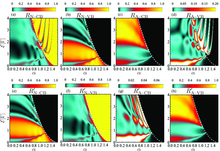
It is also worth to notice the behaviour of the two Andreev channels when injecting from the conduction band. For injection angles larger than the critical one, the VB for electrons and the CB for holes are closed; thus, the only available channels for reflection are the normal one the specular Andreev one. The amount of normal and specular Andreev reflections depend on the value of the band overlap : in fact, in the Andreev approximation, i.e., , the critical angle (8) tends to . In this limit, normal reflection and Andreev specular-reflection tend to zero. In Fig. 3 we summarise the properties we were describing above.
Moreover, in the Andreev approximation () and short junction limit , one can obtain analytical expressions for the reflection probabilities Bercioux et al. (2017) at zero injection angle:
| (21a) | ||||
| (21b) | ||||
| (21c) | ||||
| (21d) | ||||
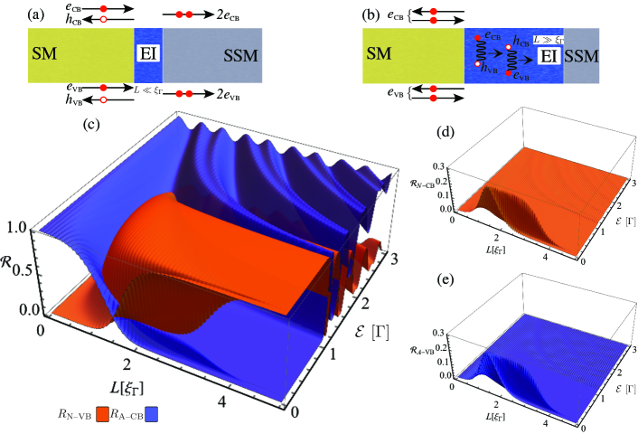
For an arbitrary length of the EI region, we show the probability for the different reflection mechanism in Fig. 4(c) to 4(e). In the limit , the behaviour corresponds to a standard hybrid junction between an SM and a two-band superconductor. We expect that an incoming electron from the CB/VB is converted into a hole of the same band and no process with a change of band will take place Blonder et al. (1982); Bercioux et al. (2017). This behaviour is also exhibited if the length of the EI region is much shorter than the coherence length : in this case, the electron can tunnel through the EI region and reach the interface with the superconductor where it is converted into a respective hole. This Andreev process is depicted in Fig. 4(a).
In the other limiting, a large EI region , the junction behaves as a single interface between an SM and an EI Rontani and Sham (2005a, b). En electron injected from the CB in order to enter the EI region needs to form an exciton pair. Thus a hole from the opposite band is required Rontani and Sham (2005a, b). As a result, an electron from the other band is retracing the path of the incoming electron [see Fig. 4(b)].
For arbitrary values of all processes have a finite probability. Specifically, we have two second-order processes: the intra-band normal reflection and the inter-band Andreev reflection. Both require the presence of a finite length EI region. The latter is always weaker than the corresponding intra-band Andreev process. Whereas inter-band normal reflection is always zero in the case of clean interface Rontani and Sham (2005a, b), it can be finite for a clean interface and a finite length of the EI region. In Fig. 4(c) we show the interplay between the inter-band normal reflection and the intra-band Andreev reflection as a function of the injection energy and the length of the EI region. In Figs. 4(d) and 4(e) we show in the same fashion the intra-band normal reflection and the inter-band Andreev reflection. It is clear that for short and long EI regions, and are the dominating processes and that only at the crossover length when they exchange role the other two channels of reflection and get a finite value.
III Differential conductance and differential resistance
In this section we use the previous results, Fig. 3, in order to describe the electronic transport properties of this hybrid junction. Our goal is to propose a direct electrical measurement scheme able to determine the size of the EI gap. At the end of the section, we provide a comparison with the experimental results by Kononov et al. Kononov et al. (2016, 2017).
III.1 Electrical characterisation of the hybrid junction
Given a finite transverse dimension , the transverse momentum gets quantized accordingly to with . In general terms, the differential conductance Blonder et al. (1982) for an NS hybrid junction in an SM system can be defined as
| (22) |
where and are the Andreev and the normal reflection probabilities, respectively, and with indicating the band index. Equation (III.1) has a pre-factor because of the two-fold spin degeneracy. In the limit of wide junctions, the spacing between different transverse modes can be considered negligible, and we can recast the sum into an integral over the (almost continuous) angle using the following transformations:
| (23) |
where we have introduced as the number of open transversal modes at energy .
Within this approximation, we can express the differential conductance as:
| (24) |
with
| (25) |
being the differential conductance of the normal state. In writing Eq. (III.1) we have used the fact that all reflection probabilities are an even function of the injection angle Beenakker (2006); Bercioux and Lucignano (2018). The conductance of the normal state will have an extra factor of due to the sum over the two open bands.
In the Andreev approximation, we can use the expressions obtained for the short junction limit, Eqs. (21) in the case of a normal injection angle (), and obtain
| (26) |
The factor is a result of the sum over the two open bands. From this expression, one sees the competition between a contribution stemming from the Andreev reflection that tends to increase the differential conductance and the appearance of the EI phase that suppresses it.
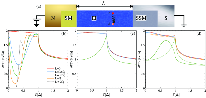
We now focus on the numerical results for arbitrary junctions. The electric configuration for measuring the differential conductance is shown in Fig. 5(a), the system is configured in a way to ground the superconducting part and have a finite voltage only on the normal contact Blonder et al. (1982). We start by showing that the presence of a finite EI region via the additional inter-band channel of normal reflection strongly influences the behaviour of the differential conductance with respect to the injection energy. In Fig. 5(b), we show the differential conductance as a function of the injection energy for different lengths of the EI region. We observe that a first consequence of not having performed the Andreev approximation neither in the SM or the SSM contact is that the differential conductance is not constant Blonder et al. (1982) for energies smaller than the superconducting gap Beenakker (2006); Bercioux and Lucignano (2018). The most remarkable result is that for a finite length of the EI region the differential conductance shows a minimum. This minimum gets deeper and moves to lower energy by increasing the length of the EI region. It is worth to note that this result is obtained in the absence of elastic reflections at the two interfaces .
The standard behaviour of an SM/SSM interface without an EI region but with finite elastic reflection potentials is shown in Fig. 5(c). It is similar to the standard results obtained by Blonder el al. Blonder et al. (1982). Increasing the value of the parameter the overall differential conductance is decreased both for energies lower and higher than the gap . This standard behaviour is very different from the one we have shown in Fig. 5(b) in the presence of the EI.
In Fig. 5(d) we show the differential conductance for . We can observe that the effect of modulation of the differential conductance due to the presence of the EI is strongly enhanced only if the first interface potential () is different from zero, whereas the second interface plays a minor role.
III.2 Comparison with the experiments
In this section we use our model to interpret experimental results of two recent works on semimetal/superconductor hybrid junctions which suggest the existence of an EI phase.
We start discussing the experiment by Kononov et al. Kononov et al. (2016), where are investigated the transport properties of a hybrid junction consisting of a HgTe QW. The width of the latter is circa 20 nm and from previous studies, the authors know that the system is an indirect SM with a small overlap between the bands Kvon et al. (2011). This property makes HgTe QWs reasonable candidates for observing the EI phase. The transport measurements showed a zero bias anomaly in the differential resistance with an energy size comparable with the estimated EI gap of the system Kononov et al. (2016).
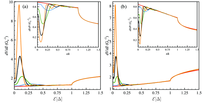
As we show next the zero bias anomaly observed experimentally is compatible with the results of the last section. In order to use our model, we need to assume that the momentum displacement between the CB and the VB is negligibly small. To evaluate the differential resistance, we take the inverse of the differential conductance in Eq. (III.1). We use the values of the system parameters given in Refs. Kvon et al. (2011); Kononov et al. (2016) and set meV, meV, meV for the Nb/HgTe structure and meV which should correspond to a (Nb/FeNi)/HgTe structure explored in Ref. Kononov et al. (2016). We also assume a finite transparency of the interface barriers Kononov et al. (2016). For these parameters value, we have an EI coherence length of nm.
The results of the differential resistance are shown in the two panels of Fig. 6 for the two different superconductor used in Ref. Kononov et al. (2016). The solid red line describes an SM/SSM junction (), and coincides with the well-known results of the Blonder-Tinkham-Klapwijk theory after integration over injection angle Blonder et al. (1982); Mortensen et al. (1999); Beenakker (2006). It is important to note that the ratio is of 2.6 and 5 for Nb (Panel a) and Nb/FeNi (Panel b), respectively. Thus the differential resistance at zero voltage is not exactly equal to , which would be the result obtained in the leading order when . By increasing the length of the EI region, we obtain a peak in the differential resistance at energies smaller than . These results resemble the experimental observations of Ref. Kononov et al. (2016) and can be attributed as a manifestation of the EI phase.
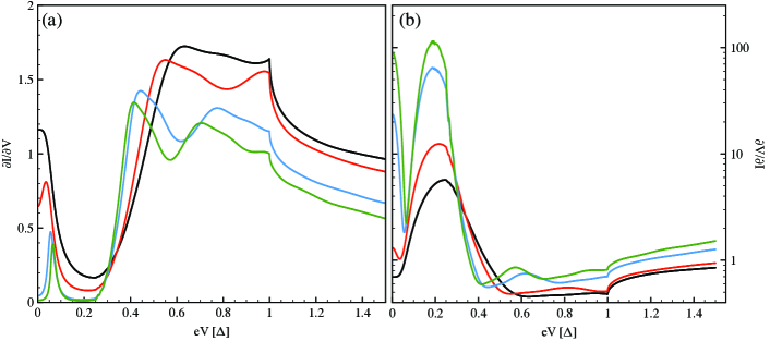
Another system that may host an EI phase are InAs/GaSb double QWs. Here, electrons are located in the InAs QW and holes are located in the GaSb QW. Recent theoretical calculations Xue and Macdonald (2018) confirmed the experimental observation that the EI phase exists in this system Du et al. (2017); Yu et al. (2018). Interestingly, the bands overlap, can be changed by changing the width of one of the QWs — this change corresponds to a modulation of in our model. We have investigated the response of the system to changes of the band overlap in Fig. 7.
Interestingly, we find at low-voltages two type of behaviors for the conductance: the one discussed previously showing a minimum in the conductance [compare black line in Fig. 7 with Fig. 6(a)], and one with a clear maximum at finite voltage (all the curves except than black in Fig. 7). These two types of behavior resemble these observed recently by Kononov at al. Kononov et al. (2017), who measured the differential resistance of a superconducting InAs/GaSb double QW junction for different with of the InAs gas. In their explanation, the different behaviors of the differential resistance is associated with the variation of the CB/VB overlap and with presence of proximitized superconducting region with a smaller gap . When changing from large to a small one, the differential conductance shows a peak at certain finite voltage. Moreover, as in the experiment of Ref. Kononov et al. (2017), the measured differential resistance of the two observed behaviors [black and green curves in Fig. 7(b)] differ by a factor larger than 20. This could also be explained from our assumption that an EI is formed between the electrodes.
It is important to stress that in our model we neglect any kind of disorder. One can expect that disorder will suppress all the effects described above for the simple reason that elastic disorder has for the EI condensate Zittartz (1967) the same effect as a low concentration of magnetic impurities has for conventional superconductivity, leading to a suppression of it. Similarly, an enhancement of temperature will wash out the non-monotonic behavior predicted for the differential conductance, as it has been seen experimentally Kononov et al. (2017). The main experimental features have been observed at the base temperature of 30 mK Kononov et al. (2016, 2017), thus justifying our approach of zero temperature.
In short, our results provide a first plausible qualitative explanation for the low-bias transport properties observed in the experiments in Refs. Kononov et al. (2016, 2017). It is however worth to mention that in addition to the low bias anomalies described above, the experiments of Ref. Kononov et al. (2016, 2017) shown also features in the sub-gap conductance that resembles the multiple-Andreev reflections processes in voltage biased Josephson junctions Averin and Bardas (1995). In principle such sub-gap features are unexpected, since in these experiments there is only one superconducting electrode. Further research is needed to understand such sub-gap behavior.
IV Conclusions & Discussion
We analyse the transport properties of a hybrid junction created in a semi-metallic system. We assume that one side of the system can be considered as a normal electrode, and the other side gets proximitized by a standard -wave superconductor. In the region between these two contacts, we consider a finite Coulomb interaction between electrons of the two bands that gives rise to an excitonic insulator. We show that the presence of the excitonic insulator can modify the transport properties of the system drastically.
Specifically, we analyse the presence of four types of reflection in the normal electrode, two normal and two Andreev reflections. We have two intra-band processes: a normal specular reflection channel and an Andreev retro-reflection one. Besides, we have also two inter-band processes: a normal retro-reflection and an Andreev specular-reflection.
The interplay of these four channels of reflections has a strong influence on the electrical properties of the system. If the length of the excitonic region is comparable to or larger than the corresponding coherence length, we observe a minimum in the differential conductance. This minimum is a signature of the presence of an EI condensate in the system. We propose our set-up for the detection of an EI condensate and we use our results for interpreting recent transport experiments in semi-metallic systems sandwiched between a normal and a superconducting contact Kononov et al. (2016, 2017).
The results we obtained are similar to the results we obtained in Ref. Bercioux et al. (2017), however, the physical contest is different, here we have considered a bulk semimetal system, whereas in Ref. Bercioux et al. (2017) we considered a bilayer system composed of two parallel two-dimensional electron gases that are hosting an excitonic insulator phase. The circuit we presented in Ref. Bercioux et al. (2017) for the detection of the excitonic insulating phase suffers from the problem of not being consistent with the survival of the excitonic insulating phase Su and Macdonald (2008).
Acknowledgements.
Discussions with J. Cayssol, V. Golovach, T.M. Klapwijk and M. Rontani are acknowledged. The work of DB, BB, and FSB is supported by Spanish Ministerio de Economía y Competitividad (MINECO) under the project FIS2014-55987-P, and by the Spanish Ministerio de Ciencia, Innovation y Universidades (MICINN) under the project FIS2017-82804-P, and by the Transnational Common Laboratory QuantumChemPhys.References
- Leggett (2006) Anthony J Leggett, Quantum Liquids, Bose Condensation and Cooper Pairing in Condensed-matter Systems (Oxford University Press, 2006).
- Leggett (2008) Anthony J Leggett, “Quantum Liquids,” Science 319, 1203–1205 (2008).
- Bardeen et al. (1957) J. Bardeen, L. N. Cooper, and J. R. Schrieffer, “Theory of superconductivity,” Phys. Rev. 108, 1175–1204 (1957).
- Mott (1961) N. F. Mott, “The transition to the metallic state,” Philos. Mag. 6, 287–309 (1961).
- Keldysh and Kopaev (1965) L. V. Keldysh and Yu. V. Kopaev, “Possible instability of the semimetallic state with respect to coulombic interaction,” Fiz. Tverd. Tela 6, 2791 (1965), [Sov. Phys. Solid State 6, 2219 (1965)].
- Jérome et al. (1967) D Jérome, T M Rice, and W Kohn, “Excitonic insulator,” Phys. Rev. 158, 462 (1967).
- Zittartz (1967) J Zittartz, “Theory of the excitonic insulator in the presence of normal impurities,” Phys. Rev. 164, 575 (1967).
- Halperin and Rice (1968) B I Halperin and T M Rice, “Possible Anomalies at a Semimetal-Semiconductor Transistion,” Rev. Mod. Phys. 40, 755–766 (1968).
- Kasprzak et al. (2006) J Kasprzak, M Richard, S Kundermann, A Baas, P Jeambrun, J M J Keeling, F M Marchetti, M H Szymańska, R André, J L Staehli, V Savona, P B Littlewood, B Deveaud, and Le Si Dang, “Bose–Einstein condensation of exciton polaritons,” Nature 443, 409–414 (2006).
- Lozovik and Yudson (1976) Y E Lozovik and V I Yudson, “New mechanism for superconductivity: pairing between spatially separated electrons and holes,” Zh. Eksp. Teor. Fiz. 71, 738 (1976), [Sov. Phys.-JETP 389, 389 (1976)].
- Shevchenko (1976) S. I. Shevchenko, “Theory of superconductivity of systems with pairing of spatially separated electrons and holes,” Fiz. Nizk. Temp. 2, 505 (1976), [Sov. J. Low-Temp. Phys. 2, 251 (1976)].
- Seradjeh et al. (2009) B Seradjeh, J E Moore, and M Franz, “Exciton Condensation and Charge Fractionalization in a Topological Insulator Film,” Phys. Rev. Lett. 103, 066402 (2009).
- Pikulin and Hyart (2014) D I Pikulin and T Hyart, “Interplay of Exciton Condensation and the Quantum Spin Hall Effect in InAs/GaSb Bilayers,” Phys. Rev. Lett. 112, 176403 (2014).
- Budich et al. (2014) Jan Carl Budich, Björn Trauzettel, and Paolo Michetti, “Time Reversal Symmetric Topological Exciton Condensate in Bilayer HgTe Quantum Wells,” Phys. Rev. Lett. 112, 146405 (2014).
- Macdonald and Rezayi (1990) A H Macdonald and E H Rezayi, “Fractional quantum Hall effect in a two-dimensional electron-hole fluid,” Phys. Rev. B 42, 3224–3227 (1990).
- Yoshioka and Macdonald (1990) Daijiro Yoshioka and Allan H. Macdonald, “Double quantum well electron-hole systems in strong magnetic fields,” J. Phys. Soc. Jpn., and J. Phys. 59, 4211–4214 (1990).
- Eisenstein and Macdonald (2004) J P Eisenstein and A H Macdonald, “Bose–Einstein condensation of excitons in bilayer electron systems,” Nature 432, 691–694 (2004).
- Spielman et al. (2000) I B Spielman, J P Eisenstein, L N Pfeiffer, and K W West, “Resonantly Enhanced Tunneling in a Double Layer Quantum Hall Ferromagnet,” Phys. Rev. Lett. 84, 5808–5811 (2000).
- Kellogg et al. (2004) M Kellogg, J P Eisenstein, L N Pfeiffer, and K W West, “Vanishing Hall Resistance at High Magnetic Field in a Double-Layer Two-Dimensional Electron System,” Phys. Rev. Lett. 93, 036801 (2004).
- Tutuc et al. (2004) E Tutuc, M Shayegan, and D A Huse, “Counterflow Measurements in Strongly Correlated GaAs Hole Bilayers: Evidence for Electron-Hole Pairing,” Phys. Rev. Lett. 93, 036802 (2004).
- Lozovik and Sokolik (2008) Y E Lozovik and A A Sokolik, “Electron-hole pair condensation in a graphene bilayer,” JETP Letters , 55 (2008).
- Min et al. (2008) Hongki Min, Rafi Bistritzer, Jung-Jung Su, and A H Macdonald, “Room-temperature superfluidity in graphene bilayers,” Phys. Rev. B 78, 121401 (2008).
- Kharitonov and Efetov (2008) Maxim Yu Kharitonov and Konstantin B Efetov, “Electron screening and excitonic condensation in double-layer graphene systems,” Phys. Rev. B 78, 241401 (2008).
- Mak et al. (2011) Kin Fai Mak, Jie Shan, and Tony F Heinz, “Seeing Many-Body Effects in Single- and Few-Layer Graphene: Observation of Two-Dimensional Saddle-Point Excitons,” Phys. Rev. Lett. 106, 046401 (2011).
- Li et al. (2016) J I A Li, T Taniguchi, K Watanabe, J Hone, A Levchenko, and C R Dean, “Negative Coulomb Drag in Double Bilayer Graphene,” Phys. Rev. Lett. 117, 046802 (2016).
- Lee et al. (2016) Kayoung Lee, Jiamin Xue, David C Dillen, Kenji Watanabe, Takashi Taniguchi, and Emanuel Tutuc, “Giant Frictional Drag in Double Bilayer Graphene Heterostructures,” Phys. Rev. Lett. 117, 046803 (2016).
- Su and MacDonald (2017) Jung-Jung Su and Allan H MacDonald, “Spatially indirect exciton condensate phases in double bilayer graphene,” Physical Review B 95, 045416 (2017).
- Burg et al. (2018) G. William Burg, Nitin Prasad, Kyounghwan Kim, Takashi Taniguchi, Kenji Watanabe, Allan H. MacDonald, Leonard F. Register, and Emanuel Tutuc, “Strongly enhanced tunneling at total charge neutrality in double-bilayer graphene- heterostructures,” Phys. Rev. Lett. 120, 177702 (2018).
- Monney et al. (2010) C Monney, E F Schwier, M G Garnier, N Mariotti, C Didiot, H Cercellier, J Marcus, H Berger, A N Titov, H Beck, and P Aebi, “Probing the exciton condensate phase in 1 T-TiSe2 with photoemission,” New J. Phys. 12, 125019–32 (2010).
- Rossnagel (2011) K Rossnagel, “On the origin of charge-density waves in select layered transition-metal dichalcogenides,” J. Phys. Condens. Matter 23, 213001 (2011).
- Kogar et al. (2017) Anshul Kogar, Melinda S Rak, Sean Vig, Ali A Husain, Felix Flicker, Young Il Joe, Luc Venema, Greg J MacDougall, Tai C Chiang, Eduardo Fradkin, Jasper van Wezel, and Peter Abbamonte, “Signatures of exciton condensation in a transition metal dichalcogenide,” Science 358, 1314–1317 (2017).
- Varsano et al. (2017) Daniele Varsano, Sandro Sorella, Davide Sangalli, Matteo Barborini, Stefano Corni, Elisa Molinari, and Massimo Rontani, “Carbon nanotubes as excitonic insulators,” Nat. Commun. 8, 1461 (2017).
- Aspitarte et al. (2017) Lee Aspitarte, Daniel R McCulley, Andrea Bertoni, Joshua O Island, Marvin Ostermann, Massimo Rontani, Gary A Steele, and Ethan D Minot, “Giant modulation of the electronic band gap of carbon nanotubes by dielectric screening,” Sci. Rep. 7, 8828 (2017).
- Senger et al. (2018) Mitchell J. Senger, Daniel R. McCulley, Neda Lotfizadeh, Vikram V. Deshpande, and Ethan D. Minot, “Universal interaction-driven gap in metallic carbon nanotubes,” Phys. Rev. B 97, 035445 (2018).
- Lu et al. (2017) Y F Lu, H Kono, T I Larkin, A W Rost, T Takayama, A V Boris, B Keimer, and H Takagi, “Zero-gap semiconductor to excitonic insulator transition in Ta¡sub¿2¡/sub¿NiSe¡sub¿5¡/sub¿,” Nat. Commun. 8, 14408 (2017).
- Mor et al. (2017) Selene Mor, Marc Herzog, Denis Golež, Philipp Werner, Martin Eckstein, Naoyuki Katayama, Minoru Nohara, Hide Takagi, Takashi Mizokawa, Claude Monney, and Julia Stähler, “Ultrafast Electronic Band Gap Control in an Excitonic Insulator,” Phys. Rev. Lett. 119, 086401 (2017).
- Kononov et al. (2016) A Kononov, S V Egorov, Z D Kvon, N N Mikhailov, S A Dvoretsky, and E V Deviatov, “Andreev reflection at the edge of a two-dimensional semimetal,” Phys. Rev. B 93, 041303 (2016).
- Kononov et al. (2017) A Kononov, V A Kostarev, B R Semyagin, V V Preobrazhenskii, M A Putyato, E A Emelyanov, and E V Deviatov, “Proximity-induced superconductivity within the InAs/GaSb edge conducting state,” Phys. Rev. B 96, 245304 (2017).
- Beenakker (2006) C Beenakker, “Specular Andreev Reflection in Graphene,” Phys. Rev. Lett. 97, 067007 (2006).
- Rontani and Sham (2005a) Massimo Rontani and L J Sham, “Coherent Transport in a Homojunction between an Excitonic Insulator and Semimetal,” Phys. Rev. Lett. 94, 186404 (2005a).
- De Gennes (1999) P G De Gennes, Superconductivity Of Metals And Alloys (Westview Press, 1999).
- Dolcini et al. (2010) Fabrizio Dolcini, Diego Rainis, Fabio Taddei, Marco Polini, Rosario Fazio, and A H Macdonald, “Blockade and Counterflow Supercurrent in Exciton-Condensate Josephson Junctions,” Phys. Rev. Lett. 104, 027004 (2010).
- Peotta et al. (2011) Sebastiano Peotta, Marco Gibertini, Fabrizio Dolcini, Fabio Taddei, Marco Polini, L B Ioffe, Rosario Fazio, and A H Macdonald, “Josephson current in a four-terminal superconductor/exciton-condensate/superconductor system,” Phys. Rev. B 84, 184528 (2011).
- Bercioux et al. (2017) D Bercioux, T M Klapwijk, and F S Bergeret, “Transport Properties of an Electron-Hole Bilayer in Contact with a Superconductor Hybrid Junction,” Phys. Rev. Lett. 119, 067001 (2017).
- Blonder et al. (1982) G E Blonder, M Tinkham, and T M Klapwijk, “Transition from metallic to tunneling regimes in superconducting microconstrictions: Excess current, charge imbalance, and supercurrent conversion,” Phys. Rev. B 25, 4515–4532 (1982).
- Ludwig (2007) T Ludwig, “Andreev reflection in bilayer graphene,” Phys. Rev. B 75, 195322 (2007).
- Efetov et al. (2015) D K Efetov, L Wang, C Handschin, K B Efetov, and J Shuang, “Specular interband Andreev reflections at van der Waals interfaces between graphene and NbSe2,” Nat. Phys. 12, 328 (2015).
- Chen et al. (2013) Wei Chen, Liang Jiang, R Shen, L Sheng, B G Wang, and D Y Xing, “Specular Andreev reflection in inversion-symmetric Weyl semimetals,” EPL 103, 27006 (2013).
- Breunig et al. (2018) Daniel Breunig, Pablo Burset, and Björn Trauzettel, “Creation of Spin-Triplet Cooper Pairs in the Absence of Magnetic Ordering,” Phys. Rev. Lett. 120, 037701 (2018).
- Bercioux and Lucignano (2018) Dario Bercioux and Procolo Lucignano, “Quasiparticle cooling using a Topological insulator-Superconductor hybrid junction,” Eur. Phys. J. Special Topics (2018), 10.1140/epjst/e2018-00069-3, [arXiv:1804.07170].
- Zehetmayer (2013) M Zehetmayer, “A review of two-band superconductivity: materials and effects on the thermodynamic and reversible mixed-state properties,” Supercond. Sci. Technol. 26, 043001 (2013).
- Rontani and Sham (2005b) Massimo Rontani and L J Sham, “Variable resistance at the boundary between semimetal and excitonic insulator,” Solid State Commun. 134, 89–95 (2005b).
- Wang et al. (2005) Baigeng Wang, Ju Peng, D Y Xing, and Jian Wang, “Spin Current due to Spinlike Andreev Reflection,” Phys. Rev. Lett. 95, 086608 (2005).
- Andreev (1964) A. F. Andreev, “Thermal conductivity of the intermediate state of superconductors,” Sov. Phys. JETP. 19 (1964).
- Zagoskin (2014) Alexandre Zagoskin, Quantum Theory of Many-Body Systems (Springer, 2014).
- Kvon et al. (2011) Z D Kvon, E B Olshanetsky, E G Novik, D A Kozlov, N N Mikhailov, I O Parm, and S A Dvoretsky, “Two-dimensional electron-hole system in HgTe-based quantum wells with surface orientation (112),” Phys. Rev. B 83, 193304 (2011).
- Mortensen et al. (1999) Niels Asger Mortensen, Karsten Flensberg, and Antti-Pekka Jauho, “Angle dependence of Andreev scattering at semiconductor–superconductor interfaces,” Phys. Rev. B 59, 10176–10182 (1999).
- Xue and Macdonald (2018) Fei Xue and A H Macdonald, “Time-Reversal Symmetry-Breaking Nematic Insulators near Quantum Spin Hall Phase Transitions,” Phys. Rev. Lett. 120, 2219 (2018).
- Du et al. (2017) Lingjie Du, Xinwei Li, Wenkai Lou, Gerard Sullivan, Kai Chang, Junichiro Kono, and Rui-Rui Du, “Evidence for a topological excitonic insulator in InAs/GaSb bilayers,” Nat. Comm. 8, 1971 (2017).
- Yu et al. (2018) W Yu, V Clericó, C Hernádendez Fuentevilla, X Shi, Y Jiang, D Saha, W K Lou, K Chang, D H Huang, G Gumbs, D Smirnov, C J Stanton, Z Jiang, V Bellani, Y Meziani, E Diez, W Pan, S D Hawkins, and J F Klem, “Anomalously large resistance at the charge neutrality point in a zero-gap inas/gasb bilayer,” New J. Phys. 20, 053062 (2018).
- Averin and Bardas (1995) D Averin and A Bardas, “ac Josephson effect in a single quantum channel,” Phys. Rev. Lett. 75, 1931 (1995).
- Su and Macdonald (2008) Jung-Jung Su and A H Macdonald, “How to make a bilayer exciton condensate flow,” Nat. Phys. 4, 799–802 (2008).