February 6, 2018; accepted May 24, 2018
Conductivity and Resistivity of Dirac Electrons in Single-Component Molecular Conductor [Pd(dddt)2]
Abstract
Dirac electrons, which have been found in the single-component molecular conductor [Pd(dddt)2] under pressure, are examined by calculating the conductivity and resistivity for several pressures of GPa, which give a nodal line semimetal or insulator. The temperature () dependence of the conductivity is studied using a tight-binding model with -dependent transfer energies, where the damping energy by the impurity scattering is introduced. It is shown that the conductivity increases linearly under pressure at low due to the Dirac cone but stays almost constant at high . Further, at lower pressures, the conductivity is suppressed due to an unconventional gap, which is examined by calculating the resistivity. The resistivity exhibits a pseudogap-like behavior even in the case described by the Dirac cone. Such behavior originates from a novel role of the nodal line semimetal followed by a pseudogap that is different from a band gap. The present result reasonably explains the resistivity observed in the experiment.
1 Introduction
Massless Dirac fermions have recently been extensively studied due to their exotic energy band with a Dirac cone. [1] Among them, Dirac electrons in molecular conductors have been found in bulk systems[2, 3] for the following two cases. One is the organic conductor -(BEDT-TTF)2I3(BEDT-TTF=bis(ethylenedithio)tetrathiafulvalene), in which a zero gap is obtained in the two-dimensional Dirac electron [4] using the tight-binding model with the transfer energy estimated by the extended Hückel method.[5, 6] The other is the single-component molecular conductor [Pd(dddt)2] (dddt = 5,6-dihydro-1,4-dithiin-2,3-dithiolate) under a high pressure, in which the unconventional Dirac electron was found by resistivity measurement[7] and first-principles calculation. [8] In fact, the latter material is a three-dimensional Dirac electron system consisting of HOMO (highest occupied molecular orbital) and LUMO (lowest unoccupied molecular orbital) functions, and exhibits a nodal line semimetal.[9]
Although there have been many studies on nodal line semimetals, [10, 11, 12] the transport property has not been studied much except for that of the molecular conductors since the behavior relevant to Dirac electrons can be obtained when the chemical potential is located close to the Dirac point. One of the remarkable characteristics of these molecular Dirac electrons is the anisotropy of the conductivity as shown for both the two-dimensional case[13] and three-dimensional case.[14] Although the conductivity at absolute zero temperature displays a universal value including the Planck constant, the theory predicts an increase in the conductivity when the temperature becomes larger than associated with the energy by the impurity scattering. However, the almost constant resistivity with varying temperature is regarded as experimental evidence of Dirac electrons. [15, 3]
Since is much smaller than the energy of the Dirac cone, it is not yet theoretically clear how to comprehend the relevance between the Dirac electrons and the constant resistivity as a function of temperature. Thus, in the present paper, we examine the temperature dependence of both the conductivity and resistivity of the Dirac electrons of the single-component molecular conductor [Pd(dddt)2] under pressure by taking into account the property of the actual band through the transfer energy of the tight-binding model.[3] Further, the characteristics of the pressure dependence of the nodal line semimetal are examined using an interpolation formula for the transfer energy between the ambient pressure and a pressure corresponding to the observed Dirac electrons.
In Sect. 2, the model is given with the formulation for the conductivity. In Sect. 3, the nodal line semimetal under pressure is explained. The temperature dependence of the anisotropic conductivity is examined using the temperature dependence of the chemical potential, which is determined self-consistently. Further, the resistivity is calculated revealing a pseudogap close to the insulating state, and compared with the experimental result. Section 4 is devoted to a summary and discussion.
2 Model and Formulation
The single component molecular conductor [Pd(dddt)2] [3] has a three-dimensional crystal structure with a unit cell which consists of four molecules (1, 2, 3, and 4) with HOMO and LUMO orbitals. The molecules are located on two kinds of layers, where layer 1 includes molecules 1 and 3 and layer 2 includes molecules 2 and 4. The transfer energies between nearest-neighbor molecules are given as follows. The interlayer energies in the direction are given by ( molecules 1 and 2 and molecules 3 and 4), and ( molecules 1 and 4 and molecules 2 and 3). The intralayer energies in the - plane are given by (molecules 1 and 3), (molecules 2 and 4), and (perpendicular to the - plane). Further, these energies are classified by three kinds of transfer energies given by HOMO-HOMO (H), LUMO-LUMO (L), and HOMO-LUMO (HL).
Based on the crystal structure,[3] the tight-binding model Hamiltonian per spin is given by
| (1) |
where are transfer energies between nearest-neighbor sites and is a state vector. and are the lattice sites of the unit cell with being the total number of square lattices, and denote the eight molecular orbitals given by the HOMO and LUMO . The lattice constant is taken as unity. For simplicity, the transfer energy at pressure (GPa) is estimated by linear interpolation between the two energies at = 8 and 0 GPa. With and GPa, the energy is written as [14]
| (2) |
The insulating state is obtained at =0 while the Dirac cone is found at by first-principles calculation,[3] corresponding to the Dirac electron indicated by the experiment. We take eV as the unit of energy. The transfer energies at = 8[3] and 0 GPa[9]), which are obtained by the extended Hückel method, are listed in Table 1. The gap between the energy of the HOMO and that of the LUMO is taken as 0.696 eV to reproduce the energy band in the first-principles calculation.
Using the Fourier transform with the wave vector , Eq. (1) is rewritten as
| (3) |
where and is expressed as The Hermite matrix Hamiltonian is given in Ref. \citenKato2017_JPSJ, where is expressed as . The quantity [] is the real matrix Hamiltonian (unitary matrix) shown in the Appendix. The nodal line has been explained using ,[16, 9] where the Dirac point is supported by the existence of an inversion center.[17] Note that gives the same conductivity as obtained from , which corresponds to a choice of the gauge. For simplicity, the following calculation of the conductivity is performed in terms of .
The energy band and the wave function , are calculated from
| (4) |
where and
| (5) |
with , and . The Dirac point is obtained from , which gives a nodal line semimetal. The insulating state is obtained for due to a half-filled band, where for all .
Using in Eq. (5), the electric conductivity per spin and per unit cell is calculated as[13, 14]
| (6) | |||||
| (7) | |||||
| (8) | |||||
where and and . and denote the Planck constant and electric charge, respectively. and denotes the chemical potential. with being the temperature in the unit of eV and . The conductivity at absolute zero temperature was examined previously by noting that .[14] The energy due to the impurity scattering is introduced to obtain a finite conductivity. The total number of lattice sites is given by , where is the number of intralayer sites and is the number of layers. Note that the calculation of Eq. (6) with the summation of at the end, i.e., the two-dimensional conductivity for a fixed , is useful to comprehend the nodal line semimetal as shown previously.[14]
The chemical potential is determined self-consistently in the clean limit from
which is the half-filled condition due to the HOMO and LUMO bands. denotes the density of states (DOS) per spin and per unit cell, which is given by
| (10) |
where . Note that Eq. (6) can be understood using the DOS when the intraband contribution () is dominant and the dependence of is small.
3 Conductivity and Resistivity of Nodal Line Semimetal in [Pd(dddt)2]
The electronic states of [Pd(dddt)2] obtained from the tight-binding model show the following pressure ( GPa) dependence. At ambient pressure ( = 0), the insulating state is found with a gap (eV) at , which separates the LUMO bands () from the HOMO bands (). With increasing , the gap decreases and becomes zero at , where the Dirac point given by emerges at . For , the minimum of the LUMO band at becomes smaller than the maximum of the HOMO band at , resulting in the following state. As shown by the effective Hamiltonian on the basis of the HOMO and LUMO orbitals,[9] a loop of the Dirac point between (conduction band) and (valence band) emerges at the intersection of the plane of and that of the vanishing of the H-L interaction (the coupling between HOMO and LUMO orbitals).[3, 9] This loop gives a semimetallic state since the chemical potential is located on a Dirac point of the loop due to a half-filled band. For , the loop exists within the first Brillouin zone (as shown by the inner loop of Fig. 1). In this case, a gap for the fixed exists at but is absent at . In fact, with decreasing from , the gap at given by decreases and becomes zero at 0.55 in the case of =7.7. Such a gap is characteristic for the loop (i.e., nodal line) within the first Brillouin zone. For , the loop exists in the extended zone (as shown by the outer loop of Fig. 1), and the gap is absent for arbitrary . Such a gap for could give rise to novel behavior in the temperature dependence of the conductivity as shown below.
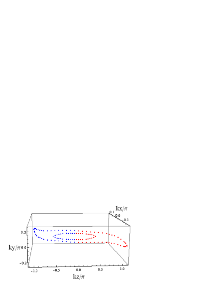
Figure 1 depicts the nodal line of the loop of the Dirac point in the three-dimensional momentum space for = 7.7 and 8, where =8 corresponds to the pressure in the experiment displaying almost constant resistivity.[3] In the previous work for = 8,[14] it was shown that the Dirac cone is anisotropic, the ratio of the velocity was estimated as , and that the conductivity is always relevant to a two-dimensional Dirac cone rotating along the loop. Thus, we mainly study as a typical conductivity in the nodal line system. Note that the semimetallic state is obtained since the chemical potential exists on the loop due to a half-filled band, for example, (= 0.5561) is located on the loop with for = 8. In fact, depends slightly on to form an energy dispersion with a width of 0.003. Further, we note that the loop is not coplanar, which is characteristic of the nodal line of the present system. We take = 1 in the following calculation.

The conductivity is determined by ( = , , and ) of Eq. (7), which is shown in Fig. 2 for = 8 and = 0.001. There are two peaks in , where the difference in magnitudes of originates from the factor in Eq. (8). These peaks correspond to the top of the HOMO band for and the bottom of the LUMO band for . This can be seen from the DOS given by Eq. (10), shown in the inset for = 8 and 7.7, where the two peaks for and come from the properties of the band edges of the HOMO and LUMO, respectively. Since the band around the edge is strongly quasi-one-dimensional along the direction, the peak is associated with the van Hove singularities of the quasi-one-dimensional band. The linear dependence around in the DOS is due to the Dirac cone, and originates from the semimetallic state of the nodal line. The behavior of the Dirac electron is found for eV, implying that the dependence of the conductivity for the Dirac electron is also expected for . The DOS outside of the peak becomes small due to the energy of the conventional band. The present calculation is performed by choosing = 0.001, which gives the following dependence. The region corresponds to the semimetallic state. The Dirac electron gives constant behavior of as a function of for , while -linear dependence is expected in the region of . For , the conductivity is determined by the effect of the energy band outside of the Dirac cone.

Figure 3 shows ( = , , and ) as a function of for = 8. The inset denotes the dependence of , which decreases monotonically, e.g., at = 0.01 for = 8. Although such a chemical potential is replaced by an averaged one in the presence of a finite , the calculation of with a chemical potential in the clean limit is reasonable for much larger than . Note that the dependence of originates from both in Eq. (6) and in of Eq. (7). The anisotropy of is large, where both and exhibit a slight maximum but increases monotonically with increasing . Typical behavior of the Dirac cone is seen for , which increases linearly at low temperatures. For comparison, the intraband contribution is shown by the dot-dashed line, which is obtained for . The interband contribution is obtained by the difference between (solid line) and . The increase in as a function of is determined by the intraband contribution while close to =0 is determined by both intra- and interband contributions. Since the maximum of corresponds to that of in Fig. 2, the maximum suggests a crossover from the Dirac electron to the conventional electron. We also calculated by fixing at = 0 to see the effect of the variation of on the conductivity. Such is slightly smaller than that of the solid line but is still located above the dot-dashed line in Fig. 3. Thus, it turns out that the increase in at low temperatures () originates from a property of the Dirac cone, and the almost -independent at higher is obtained due to the suppression of the effect of the Dirac cone by the conventional band.
We note at =0 in the presence of both the Dirac cone and the nodal line. Based on the previous calculation,[18] a simplified model of a Dirac cone with a chemical potential defined by an averaged gives , where the first term corresponds to the universal conductivity. Thus, the decrease in gives the increase in , which is also verified numerically.

In Fig. 4, the dependence of is examined for = 8, 7.7, 7.58, and 7.5. The inset shows the corresponding at =0. Compared with = 8, the nodal line for =7.7 is reduced as shown by the inner loop of Fig. 1, since a gap exists on the - plane for a fixed with . Thus, given by the dotted line in the inset decreases for small , leading to the suppression of (dotted line) at low temperatures. This can also be seen from the DOS (inset of Fig. 2). The linear increase in in the case of = 8 diminishes and is replaced by pseudogap behavior. For = 7.58, corresponding to the onset of the loop, the pseudogap behavior is further enhanced, where the suppression becomes larger but still remains due to . For = 7.5, exhibits behavior expected in the insulating state. The gap at = 0 is estimated as from the energy bands and . The effect of still remains, as seen from the inset, where for and for . Note that of the nodal line semimetal for = 7.7 and 7.58 is characterized by such pseudogap behavior at lower temperatures in addition to a slight maximum at higher temperatures.

Now we examine the behavior of for , which corresponds to the region described by the Dirac cone. Instead of , we calculate the resistivity, which is obtained by due to the off-diagonal element being much smaller than the diagonal element.[14] The dependence of log() (base 10 logarithm) as a function of is shown in Fig. 5 for = 8, 7.7, 7.58, and 7.5, the same values as in Fig. 4. With decreasing , the increase in becomes steep due to the reduction of and the increase in the gap. For =7.5, behavior of the insulating state is seen, where suggests an activation gap. With increasing , this gap decreases while the following characteristic appears as a nodal line semimetal. The tangent of , which is constant for small , begins to decrease at (eV)-1 and slowly varies in the region where the energy corresponds to the semimetal and . Thus, there are two regions (I) and (II). Gap behavior occurs in region (I) given by (i.e., ) while semimetallic behavior occurs in region (II) given by (i.e., ). We define the gap by in region (I). The gap with some choices of is shown in the inset, which is estimated from the main figure in Fig. 5 at (eV)-1 (). The dashed line in the inset denotes the band gap , which is defined by for arbitrary . With increasing , ( 0.041) at = 0 decreases linearly and becomes zero at = 7.58. The gap decreases as a function of but deviates from the -linear dependence and remains finite even at = 8. The gap at = 7.5 corresponds well to , while and at = 7.58. For = 7.7, the gap in region (I) is further reduced. The metallic contribution in region (II) originates from the nodal line, for , which is enhanced by , as seen from in the inset of Fig. 4. Thus, pseudogap behavior is expected, i.e., the coexistence of the semimetallic component and the gap for . For = 8, where the nodal line exists for arbitrary , the crossover still exists but the boundary between region (I) and region (II) is invisible. Thus, such dependence of the gap shows a crossover from the insulating gap to the pseudogap at .
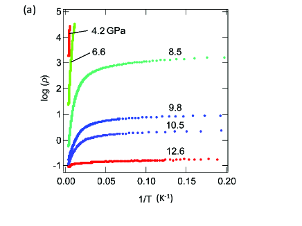
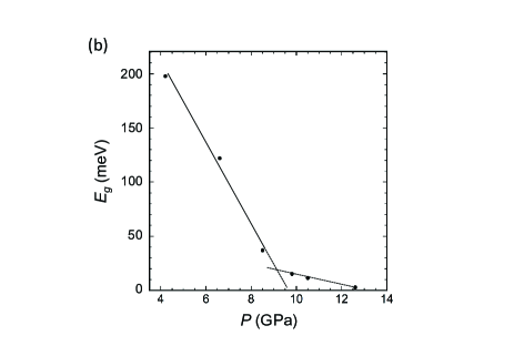
Here we compare the present result of with that observed in the experiment on [Pd(dddt)2], where the dc resistivity was measured along the longest side of the crystal (parallel to the direction). [3]. Figure 6(a), obtained from Ref. \citenKato_JACS, depicts the dependence of , where log() is shown as a function of for several choices of . These behaviors are also classified into two cases. For small , the tangent of log() as a function of is large [region (I)], whereas it is small for large [region (II)]. The temperature which separates region (I) from region (II) is about K for = 8.5, 9.8, 10.5, and 12.6 GPa. For = 4.2 and 6,6 GPa, is observed only in region (I). The gap , which is obtained from the tangent in region (I), is shown in Fig. 6(b). Two lines are drawn to guide the eye, where the line at lower pressures indicates a band gap. The gap at higher pressures exhibits a dependence different from that at lower pressures, suggesting a nontrivial origin. Figures 6(a) and 6(b) are compared with Fig. 5. The dependence of log() at =12.6 in the former corresponds to that of = 8 in the latter. It is found that the crossover temperature between region (I) and region (II) is comparable but the magnitude of in the experiment is much larger than of the theory. The cases for = 9.8 and 10.5 GPa in Fig. 6(a) suggest a state followed by the pseudogap of the nodal line semimetal.
4 Summary and Discussion
We have examined the temperature dependence of the resistivity using the conductivity for Dirac electrons in [Pd(dddt)2], which exhibits a nodal line semimetal. The main results are as follows.
(i) For a pressure = 8 corresponding to the Dirac electron observed in the experiment, a -linear increase in is obtained at low temperatures, whereas is almost constant at high temperatures. The former originates from the Dirac cone and the latter is due to the finite DOS of the conventional band outside of the Dirac cone. The ratio obtained for = 0.001 is similar to that in the experiment.[3] Note that depends on since the ratio is given by 3.1, 2.0, 1.4, and 0.87 for = 0.0005, 0.001, 0.002, and 0.004, respectively, suggesting a reasonable choice of =0.001 to comprehend the results of the experiment. (ii) With decreasing , decreases due to the decrease in the loop of the nodal line and the increase in the gap, as seen from the calculation of for a fixed . [14] For = 7.7, the nodal line exists for and is absent for . This gives pseudogap behavior in since the former gives a semimetal and the latter gives a gap. Such a magnitude of the gap , which is estimated from the tangent of the log()-1/ plot, is different from the band gap and is characteristic of a nodal line semimetal close to the insulating state. (iii) The calculation of using the tight-binding model is compared with that obtained experimentally and qualitatively good agreement is found. The experimental results are understood as evidence of a nodal line semimetal, where the loop of the Dirac point gives pseudogap behavior depending on the pressure.
We discuss the agreement between the experiment and theory. Our tight-binding model with the transfer energies well qualitatively describes the pressure and temperature dependence of the conductivity, but the determination of the absolute value is beyond the present scheme due to the Hückel approximation. For further comparison, it will be useful to observe the resistivity perpendicular to the present direction corresponding to the longest size of the crystal since large anisotropy is predicted by the theory.
In addition to the energy band, the topological property of the wave function given by the Berry phase[19] is important for understanding the Dirac nodal line. The Berry curvature of two-dimensional Dirac electrons shows a peak around the Dirac point, which also occurs for graphene and organic conductors.[20, 21] However, that of the nodal line is complicated due to the three-dimensional behavior, where the direction of the curvature rotates along the line. The Berry phase with a component parallel to the magnetic field could contribute to observe the Hall conductivity, which is expected to be different from that in two dimensions.[1, 22]
Acknowledgements.
One of the authors thanks T. Tsumuraya and A. Yamakage for useful discussions on the nodal line semimetal. This work was supported by JSPS KAKENHI Grant Numbers JP15H02108 and JP16H06346.Appendix A Matrix elements of Hamiltonian
We show explicitly the real matrix obtained from in Ref. \citenKato2017_JPSJ using a unitary transformation given by , where has only the diagonal matrix elements given by , , , , , , , and with , and . Since the symmetry of the HOMO (LUMO) is odd (even) with respect to the Pd atom, the matrix elements of H-L ( with , and ) are odd functions with respect to , i.e., antisymmetric at the time-reversal-invariant momentum.
The real matrix elements () are shown in Table 2, where the matrix elements of are divided into the 4 x 4 matrices, , , corresponding to the H-H, H-L and L-L components, respectively. The functions in Table 2 are defined by , , , , and with , , and , where * denotes .
References
- [1] K. S. Novoselov, A. K. Geim, S. V. Morozov, D. Jiang, M. I. Katsnelson, I. V. Grigorieva, S. V. Dubonos, and A. A. Firsov, Nature 438, 197 (2005).
- [2] K. Kajita, Y. Nishio, N. Tajima, Y. Suzumura, and A. Kobayashi, J. Phys. Soc. Jpn. 83, 072002 (2014).
- [3] R. Kato, H. B. Cui, T. Tsumuraya, T. Miyazaki, and Y. Suzumura, J. Am. Chem. Soc. 139, 1770 (2017).
- [4] S. Katayama, A. Kobayashi, and Y. Suzumura, J. Phys. Soc. Jpn. 75, 054705 (2006).
- [5] T. Mori, A. Kobayashi, Y. Sasaki, H. Kobayashi, G. Saito, and H. Inokuchi, Chem. Lett. 13, 957 (1984).
- [6] R. Kondo, S. Kagoshima, and J. Harada, Rev. Sci. Instrum. 76, 093902 (2005).
- [7] H. Cui, T. Tsumuraya, Y. Kawasugi, and R. Kato, presented at 17th Int. Conf. High Pressure in Semiconductor Physics (HPSP-17), 2016.
- [8] T. Tsumuraya, H. Cui, T. Miyazaki, and R. Kato, presented at Meet. Physical Society Japan, 2014; T. Tsumuraya, H. Kino, R. Kato, and T. Miyazaki, private communication.
- [9] R. Kato and Y. Suzumura, J. Phys. Soc. Jpn. 86, 064705 (2017).
- [10] S. Murakami, New J. Phys. 9 356 (2007).
- [11] A. A. Burkov, M. D. Hook, and L. Balents, Phys. Rev. B 84 235126 (2011).
- [12] A. Yamakage, Y. Yamakawa, Y. Tanaka, and Y. Okamoto, J. Phys. Soc. Jpn. 85, 013708 (2016).
- [13] S. Katayama, A. Kobayashi, and Y. Suzumura, J. Phys. Soc. Jpn. 75, 023708 (2006).
- [14] Y. Suzumura, J. Phys. Soc. Jpn. 86, 124710 (2017).
- [15] N. Tajima, S. Sugawara, M. Tamura, R. Kato, Y. Nishio, and K. Kajita, EPL 80, 47002 (2007).
- [16] Y. Suzumura, J. Phys. Soc. Jpn. 85, 053708 (2016).
- [17] C. Herring, Phys. Rev. 52, 365 (1937).
- [18] Y. Suzumura, I. Proskurin, and M. Ogata, J. Phys. Soc. Jpn. 83, 023701 (2014).
- [19] M. V. Berry, Proc. R. Soc. London, Ser. A 392, 45 (1984).
- [20] J. N. Fuchs, F. Piechon, M. O. Goerbig, and G. Montambaux, Eur. Phys. J. B 77, 351 (2010).
- [21] Y. Suzumura and A. Kobayashi, J. Phys. Soc. Jpn. 80, 104701 (2011).
- [22] N. Tajima, T. Yamauchi, T. Yamaguchi, M. Suda, Y. Kawasugi, H. M. Yamamoto, R. Kato, Y. Nishio, and K. Kajita, Phys. Rev. B 88, 075315 (2013).
Note added in proof
We noticed that another group [Z. Liu, H. Wang, Z. F. Wang, J. Yang, and F. Liu, Phys. Rev. B 97, 155138 (2018)] performed the first-principles band calculation using our structural data[3] and reconfirmed the nodal line semimetal character of [Pd(dddt)2].