Center for Nanostructured Graphene (CNG), Technical University of Denmark
The Computational 2D Materials Database: High-Throughput Modeling and Discovery of Atomically Thin Crystals
Abstract
We introduce the Computational 2D Materials Database (C2DB), which organises a variety of structural, thermodynamic, elastic, electronic, magnetic, and optical properties of around 1500 two-dimensional materials distributed over more than 30 different crystal structures. Material properties are systematically calculated by density functional theory and many-body perturbation theory (G0W0 and the Bethe-Salpeter Equation for 250 materials) following a semi-automated workflow for maximal consistency and transparency. The C2DB is fully open and can be browsed online at c2db.fysik.dtu.dk or downloaded in its entirety. In this paper, we describe the workflow behind the database, present an overview of the properties and materials currently available, and explore trends and correlations in the data. Moreover, we identify a large number of new potentially synthesisable 2D materials with interesting properties targeting applications within spintronics, (opto-)electronics, and plasmonics. The C2DB offers a comprehensive and easily accessible overview of the rapidly expanding family of 2D materials and forms an ideal platform for computational modeling and design of new 2D materials and van der Waals heterostructures.
1 Introduction
Over the past decade, atomically thin two-dimensional (2D) materials have made their way to the forefront of several research areas including batteries, (electro-)catalysis, electronics, and photonics1, 2. This development was prompted by the intriguing and easily tunable properties of atomically thin crystals and has been fueled by the constant discovery of new 2D materials and the emergent concepts of lateral3 and vertical4 2D heterostructures, which opens completely new possibilities for designing materials with tailored and superior properties.
So far more than fifty compounds have been synthesised or exfoliated as single layers (see Figure 7). These include the well known monoelemental crystals (Xenes, e.g. graphene, phosphorene)5 and their ligand functionalised derivatives (Xanes, e.g. CF, GeH)6, transition metal dichalcogenides (TMDCs, e.g. MoS2, TaSe2)7, transition metal carbides and -nitrides (MXenes, e.g. Ti2CO2)8, group III-V semiconductors and insulators (e.g. GaN, BN)9, 10, transition metal halides (e.g. CrI3)11, 12, post-transition metal chalcogenides (e.g. GaS and GaSe)13, 14 and organic-inorganic hybrid perovskites (e.g. Pb(C4H9NH3)2I4)15. However, the already known monolayers are only the tip of a much larger iceberg. Indeed, recent data mining studies indicate that several hundred 2D materials could be exfoliated from known layered bulk crystals16, 17, 18, 19. In the present work we take a complementary approach to 2D materials discovery based on combinatorial lattice decoration and identify another few hundred previously unknown and potentially synthesisable monolayers.
In the search for new materials with tailored properties or novel functionalities, first-principles calculations are playing an increasingly important role. The continuous increase in computing power and significant advancements of theoretical methods and numerical algorithms have pushed the field to a point where first-principles calculations are comparable to experiments in terms of accuracy and greatly surpass them in terms of speed and cost. For more than a century, experimental databases on e.g. structural, thermal, and electronic properties, have been a cornerstone of materials science, and in the past decade, the experimental data have been augmented by an explosion of computational data obtained from first-principles calculations. Strong efforts are currently being focused on storing and organising the computational data in open repositories20, 21. Some of the larger repositories, together containing millions of material entries, are the Materials Project22, the Automatic Flow for Materials Discovery (AFLOWLIB)23, the Open Quantum Materials Database (OQMD)24, 25, and the Novel Materials Discovery (NOMAD) Repository26.
The advantages of computational materials databases are many. Most obviously, they facilitate open sharing and comparison of research data whilst reducing duplication of efforts. In addition, they underpin the development and benchmarking of new methods by providing easy access to common reference systems27. Finally, the databases enable the application of machine learning techniques to identify deep and complex correlations in the materials space and to use them for designing materials with tailored properties and for accelerating the discovery of new materials28, 29, 30. Among the challenges facing the computational databases is the quality of the stored data, which depends both on the numerical precision (e.g. the employed -point grid and basis set size) and the accuracy of the employed physical models (e.g. the exchange-correlation functional). Most of the existing computational databases store results of standard density functional theory (DFT) calculations. While such methods, when properly conducted, are quite reliable for ground state properties such as structural and thermodynamic properties, they are generally not quantitatively accurate for excited state properties such as electronic band structures and optical absorption spectra.
Compared to databases of bulk materials, databases of 2D materials are still few and less developed. Early work used DFT to explore the stability and electronic structures of monolayers of group III-V honeycomb lattices31, 32 and the class of MX2 transition metal dichalcogenides and oxides33. Later, by data-filtering the inorganic crystal structure database (ICSD), 92 experimentally known layered crystals were identified and their electronic band structures calculated at the DFT level34. Another DFT study, also focused on stability and band structures, explored around one hundred 2D materials selected from different structure classes35. To overcome the known limitations of DFT, a database with many-body G0W0 band structures for 50 semiconducting TMDCs was established36. Very recently, data mining of the Materials Project and experimental crystal structure databases in the spirit of Ref. 34, led to the identification of close to one thousand experimentally known layered crystals from which single layers could potentially be exfoliated17, 16, 18, 19. These works also computed basic energetic, structural and electronic properties of the monolayers (or at least selected subsets) at the DFT level.
In this paper, we introduce the open Computational 2D Materials Database (C2DB) which organises a variety of ab-initio calculated properties for more than 1500 different 2D materials. The key characteristics of the C2DB are:
-
•
Materials: the database focuses entirely on 2D materials, i.e. isolated monolayers, obtained by combinatorial lattice decoration of known crystal structure prototypes.
-
•
Consistency: all properties of all materials are calculated using the same code and parameter settings following the same workflow for maximum transparency, reproducibility, and consistency of the data.
-
•
Properties: the database contains a large and diverse set of properties covering structural, thermodynamic, magnetic, elastic, electronic, dielectric and optical properties.
-
•
Accuracy: Hybrid functionals (HSE06) as well as beyond-DFT many-body perturbation theory (G0W0) are employed to obtain quantitatively accurate band structures, and optical properties are obtained from the random phase approximation (RPA) and Bethe-Salpeter Equation (BSE).
-
•
Openness: the database is freely accessible and can be directly downloaded and browsed online using simple and advanced queries.
The systematic combinatorial approach used to generate the structures in the database inevitably produces many materials that are unstable and thus unrealistic and impossible to synthesise in reality. Such “hypothetical” structures may, however, still be useful in a number of contexts, e.g. for method development and benchmarking, testing and training of machine learning algorithms, identification of trends and structure-property relationships, etc. For this reason we map out the properties of all but the most unstable (and thus chemically unreasonable) compounds. Nevertheless, the reliable assessment of stability and synthesisability of the candidate structures is an essential issue. Using the 55 materials in the C2DB, which have been experimentally synthesised in monolayer form, as a guideline, we set down the criteria that a hypothesised 2D material should fulfill in order for it to be “likely synthesisable”. On the basis of these criteria, we introduce a simple stability scale to quantify a candidate material’s dynamic and thermodynamic stability. Out of an initial set of more than 1900 monolayers distributed over 32 different crystal structures, we find 350 in the most stable category. In addition to the 55 experimentally synthesised monolayers, this set also includes around 80 monolayers from experimentally known vdW layered bulk materials, and thus around 200 completely new and potentially synthesisable 2D materials.
In Section 2, we describe the computational workflow behind the database. The structure and properties of the materials are calculated using well established state-of-the-art methodology. Technical descriptions of the different steps in the workflow are accompanied by illustrative examples and comparisons with literature data. Since documentation and validation is the main purpose of the section, we deliberately focus on well known 2D materials like the Xenes and transition metal dichalcogenides where plenty of both computational and experimental reference data is available. It should be clear that the novelty of the present work does not lie in the employed methodology nor in the type of materials properties that we calculate. The significance of our work is rather reflected by the fact that when large and consistently produced data sets are organised and made easily accessible, new scientific opportunities arise. As outlined below, this paper presents several examples of this effect.
In Section 3 we give an overview of the materials and the data contained in the C2DB and provide some specific examples to illustrate its use. Using an extensive set of many-body G0W0 calculations as a reference, we establish the performance of various DFT xc-functionals for predicting band gaps, band edge positions, and band alignment at hetero-interfaces, and we propose an optimal strategy for obtaining accurate band energies at low computational cost. Similarly, the 250 BSE calculations allow us to explore trends in exciton binding energies and perform a statistically significant and unbiased assessment of the accuracy and limitations of the widely used Mott-Wannier model for 2D excitons. From the data on more than 600 semiconductor monolayers, we present strong empirical evidence against an often employed relation between effective masses and band gaps derived from perturbation theory. Inspired by the potential of using 2D materials as building blocks for plasmonics and photonics, we propose a model to predict the plasmon dispersion relations in 2D metals from the (intraband) plasma frequency and the onset of interband transitions and use it to identify 2D metals with plasmons in the optical frequency regime. We propose several new magnetic 2D materials (including both metals and semiconductors) with ferromagnetic or anti-ferromagnetic ordering and significant out-of-plane magnetic anisotropy. Finally, we point to new high-mobility 2D semiconductors including some with band gaps in the range of interest for (opto)electronic applications.
In Section 4 we provide our conclusions together with an outlook discussing some opportunities and possible future directions for the C2DB.
2 Workflow
The workflow used to generate the data in the C2DB is illustrated in Figure 1. It consists of two parts: In the first part (left panel) the unit cell and atom positions are optimised for different magnetic configurations: non-magnetic (NM), ferro-magnetic (FM) and antiferro-magnetic (AFM). Materials satisfying certain stability and geometry criteria (indicated by green boxes) are subject to the second part (right panel) where the different properties are computed using DFT and many-body methods. The G0W0 band structure and BSE absorbance calculations have been performed only for semiconducting materials with up to four atoms in the unit cell. Per default, properties shown in the online database include spin-orbit coupling (SOC); however, to aid comparison with other calculations, most properties are also calculated and stored without SOC.
All DFT and many-body calculations are performed with the projector augmented wave code GPAW 37 using plane wave basis sets and PAW potentials version 0.9.2. The workflow is managed using the Python based Atomic Simulation Environment (ASE)38. We have developed a library of robust and numerically accurate (convergence verified) ASE-GPAW scripts to perform the various tasks of the workflow, and to create the database afterwards. The library is freely available, under a GPL license.
Below we describe all steps of the workflow in detail. As the main purpose is to document the workflow, the focus is on technical aspects, including numerical convergence and benchmarking. An overview of the most important parameters used for the different calculations is provided in Table 1.
| Workflow step(s) | Parameters |
|---|---|
| Structure and energetics (1-4)† | vacuum = 15 Å; -point density = 6.0/Å-1; Fermi smearing = 0.05 eV; PW cutoff = 800 eV; xc functional = PBE; maximum force = 0.01 eV/Å; maximum stress = 0.002 eV/Å3; phonon displacement = 0.01Å |
| Elastic constants (5) | -point density = ; strain = 1% |
| Magnetic anisotropy (6) | -point density = ; spin-orbit coupling = True |
| PBE electronic properties (7-10 and 12) | -point density = ( for step 7) |
| Effective masses (11) | -point density = ; finite difference |
| Deformation potential (13) | -point density = 12.0/Å-1; strain = 1% |
| Plasma frequency (14) | -point density = 20.0/Å-1; tetrahedral interpolation |
| HSE band structure (8-12) | HSE06@PBE; -point density = 12.0/Å-1 |
| G0W0 band structure (8, 9) | G0W0@PBE; -point density = ; PW cutoff = (extrapolated from 170, 185 and 200 eV); full frequency integration; analytical treatment of for small ; truncated Coulomb interaction |
| RPA polarisability (15) | RPA@PBE; -point density = ; PW cutoff = 50 eV; truncated Coulomb interaction; tetrahedral interpolation |
| BSE absorbance (16) | BSE@PBE with G0W0 scissors operator; -point density = ; PW cutoff = 50 eV; truncated Coulomb interaction; at least 4 occupied and 4 empty bands |
| †For the cases with convergence issues, we set a -point density of 9.0 and a smearing of 0.02 eV. | |
2.1 Structure relaxation
The workflow is initiated with a crystal structure defined by its unit cell (Bravais lattice and atomic basis). The crystal lattice is typically that of an experimentally known prototype (the “seed structure”) decorated with atoms picked from a subset of the periodic table, see Figure 2. We refer to materials by the chemical formula of their unit cell followed by the crystal structure. The latter is indicated by a representative material of that prototype, as described in Sec 3.1. For example, monolayer MoS2 in the hexagonal H and T phases are denoted MoS2-MoS2 and MoS2-CdI2, respectively. Now, MoS2 is in fact not stable in the T phase, but undergoes a distortion to the so-called T′ phase. Because the T′ phase is the thermodynamically stable phase of WTe2, we denote MoS2 in the distorted T phase by Mo2S4-WTe2. In the following, we shall refer to the unit cell with which the workflow is initiated, i.e. the unit cell of the seed structure, as the primitive cell or the cell, even if this cell is not dynamically stable for the considered material (see Section 2.4).
The unit cell and internal coordinates of the atoms are relaxed in both a spin-paired (NM), ferromagnetic (FM), and anti-ferromagnetic (AFM) configuration. Calculations for the AFM configuration are performed only for unit cells containing at least two metal atoms. The symmetries of the initial seed structure are kept during relaxation. All relevant computational details are provided in Table 1.
After relaxation, we check that the structure has remained a covalently connected 2D material and not disintegrated into 1D or 0D clusters. This is done by defining clusters of atoms using the covalent radius39 + 30% as a measure for covalent bonds between atoms. The dimensionality of a cluster is obtained from the scaling of the number of atoms in a cluster upon repetition of the unit cell following the method described by Ashton et al. 40. Only materials containing exactly one cluster of dimensionality 2 are given further consideration (an exception is made for the metal-organic perovskites (prototype PbA2I4) for which the metal atom inside the octahedron represents a 0D cluster embedded in a 2D cluster). To illustrate the effect of the covalent radius + 30% threshold, Figure 3 shows the distribution of the candidate structures in the database as a function of the covalent factor needed to fully connect the structure. Most materials have a critical covalent factor below 1.3 and fall in the green shaded region. There is, however, a tail of around 100 disconnected materials (red region); these materials are not included in the database.
We also check that the material is not already contained in the database. This is done by measuring the root mean square distance (RMSD)41 relative to all other materials in the C2DB with the same reduced chemical formula. A threshold of 0.01 Å is used for this test.
In case of multiple metastable magnetic configurations (in practice, if both a FM and AFM ground state are found), these are regarded as different phases of the same material and will be treated separately throughout the rest of the workflow. To indicate the magnetic phase we add the extensions “FM” or “AFM” to the material name. The total energy of the spin-paired ground state is always stored, even when it is not the lowest. If the energy of the non-magnetic state is higher than the most stable magnetic state by less than 10 meV/atom, the workflow is also performed for the non-magnetic state. This is done in recognition of the finite accuracy of DFT for predicting the correct energetic ordering of different magnetic states.
We have compared the lattice constants of 29 monolayers with those reported in Ref. 42, which were obtained with the VASP code using PBE and very similar numerical settings and find a mean absolute deviation of 0.024 Å corresponding to 0.4%. The small yet finite deviations are ascribed to differences in the employed PAW potentials.
2.2 Crystal structure classification
2.2.1 Symmetry
To classify the symmetries of the crystal structure the 3D space group is determined using the crystal symmetry library Spglib43 on the 3D supercell with a tolerance of Å.
2.2.2 Prototypes
The materials are classified into crystal structure prototypes based on the symmetry of the crystals. For two materials to belong to the same prototype, we require that they have the same space group, the same stoichiometry, and comparable thicknesses. The last requirement is included to distinguish between materials with the same symmetry and stoichiometry but with different number of atomic layers, see for example monolayer hBN and GaS in Figure 4. Each prototype is labelled by a specific representative material. For prototypes which have been previously investigated, we comply with the established conventions. However, since the field of 2D materials is still young and because C2DB contains a large number of never-synthesised materials, some of the considered crystal structures fall outside the known prototypes. In these cases we have chosen the representative material to be the one with the lowest energy with respect to the convex hull. Some of the crystal structure prototypes presently contained in the C2DB are shown in Figure 4.
2.3 Thermodynamic stability
The heat of formation, , is defined as the energy of the material with respect to the standard states of its constituent elements. For example, the heat of formation per atom of a binary compound, AxBy, is
| (1) |
where is the total energy of the material AxBy, and and are the total energies of the elements A and B in their standard state. When assessing the stability of a material in the C2DB, it should be kept in mind that the accuracy of the PBE functional for the heat of formation is only around 0.2 eV/atom on average44. Other materials databases, e.g. OQMD, Materials Project, and AFLOW, employ fitted elementary reference energies (FERE)45 and apply a Hubbard term 46 for the rare earth and transition metal atoms (or a selected subset of them). While such correction schemes in general improve they also introduce some ambiguity, e.g. the dataset from which the FERE are determined or the exact form of the orbitals on which the term is applied. Thus in order not to compromise the transparency and reproducibility of the data we use the pure PBE energies.
For a material to be thermodynamically stable it is necessary but not sufficient that . Indeed, thermodynamic stability requires that be negative not only relative to its pure elemental phases but relative to all other competing phases, i.e. its energy must be below the convex hull.47 We stress, however, that in general, but for 2D materials in particular, this definition cannot be directly applied as a criterion for stability and synthesisability. The most important reasons for this are (i) the intrinsic uncertainty on the DFT energies stemming from the approximate xc-functional (ii) substrate interactions or other external effects that can stabilise the monolayer (iii) kinetic barriers that separate the monolayer from other lower energy phases rendering the monolayer (meta)stable for all practical purposes.
We calculate the energy of the 2D material relative to the convex hull of competing bulk phases, . The convex hull is currently constructed from the 2836 most stable binary bulk compounds which were obtained from the OQMD24. The energies of the bulk phases were recalculated with GPAW using the PBE xc-functional and the same numerical settings as applied for the 2D materials (but the structure was not re-optimised). Because the bulk reference structures from OQMD were optimised with the VASP code and with Hubbard -corrections for materials containing 3 elements, and because the PBE misses attractive vdW interaction, the bulk energies could be slightly overestimated relative to the monolayers. As a consequence, monolayers that also exist in a layered bulk phase could have , even if the layered bulk phase is part of the convex hull and thus should be energetically more stable than the monolayer. Comparing our values for 35 compounds with the exfoliation energies calculated in Ref. 18 employing vdW compliant xc-functionals for both bulk and monolayer, we estimate the errors in the convex hull energies to be below 0.1 eV/atom.
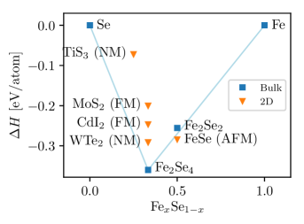
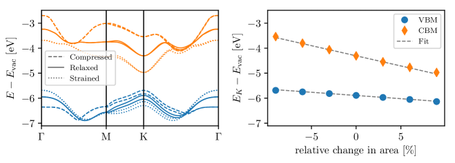
As an example, the convex hull for FexSe1-x is shown in Figure 5. The convex hull as defined by the bulk binaries is indicated by the blue lines. The labels for the 2D materials refer to the crystal prototype and magnetic order. Clearly, most 2D materials lie above the convex hull and are thus predicted to be thermodynamically unstable in freestanding form under standard conditions. However, as mentioned above, depending on the material, errors on the PBE formation energies can be sizable and thus the hull diagram should only be taken as guideline. Nevertheless, in the present example we find that FeSe (which is itself a prototype) with anti-ferromagnetic ordering lies slightly below the convex hull and is thus predicted to be thermodynamically stable. This prediction is consistent with the recent experimental observation that monolayer FeSe deposited on SrTiO3 exhibits AFM order48.
2.4 Phonons and dynamic stability
Due to the applied symmetry constraints and/or the limited size of the unit cell, there is a risk that the structure obtained after relaxation does not represent a local minimum of the potential energy surface, but only a saddle point. We test for dynamical stability by calculating the -point phonons of a repeated cell (without re-optimising the structure) as well as the elastic constants (see Section 2.5). These quantities represent second-order derivatives of the total energy with respect to atom displacements and unit cell lengths, respectively, and negative values for either quantity indicate a structural instability.
The -point phonons of the supercell are obtained using the finite displacement method49. We displace each atom in the primitive cell by Å , and calculate the forces induced on all the atoms in the supercell. From the forces we construct the dynamical matrix, which is diagonalised to obtain the -point phonons of the cell (or equivalently the -point and zone boundary phonons of the primitive cell). The eigenvalues of the dynamical matrix correspond to the square of the mass-renormalised phonon frequencies, . Negative eigenvalues are equivalent to imaginary frequencies and signal a saddle point.
Our procedure explicitly tests for stability against local distortions of periodicities up to and thus provides a necessary, but not sufficient condition for dynamic stability. We stress, however, that even in cases where a material would spontaneously relax into a structure with periodicity larger than , the -point dynamical matrix of the cell could exhibit negative eigenvalues. Our test is thus more stringent than it might seem at first glance. In principle, a rigorous test for dynamic stability would require the calculation of the full phonon band structure. Mathematically, the instabilities missed by our approach are those that result in imaginary phonons in the interior of the BZ but not at the zone boundary. Physically, such modes could be out of plane buckling or charge density wave-driven reconstructions with periodicities of several unit cells. In general, these types of instabilities are typically rather weak (as measured by the magnitude of the imaginary frequency) as compared to more local distortions such as the T to T′ distortion considered below. Moreover, they could well be a special property of the isolated monolayer and become stabilised by the ubiquitous interactions of the 2D material with its environment, e.g. substrates. This is in fact supported by the full phonon calculations by Mounet et al. for isolated monolayers predicted to be easily exfoliable from experimentally known layered bulk phases18. Indeed, most of the instabilities revealed by their calculations are of the type described above and would thus be missed by our test. However, these instabilities cannot be too critical as the monolayers are known to be stable in the vdW bonded layered bulk structure.
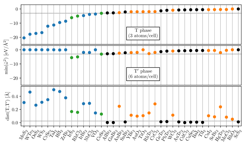
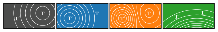
As an example, Figure 6 compares the dynamical stability of a subset of transition metal dichalcogenides and -oxides in the T and T′ phases (CdI2 and WTe2 prototypes). The two upper panels show the smallest eigenvalue of the -point dynamical matrix of the cell. Only materials above the dashed line are considered dynamically stable (for this example we do not consider the sign of the elastic constants which could further reduce the set of dynamically stable materials). Since the unit cell of the T′ phase contains that of the T phase it is likely that a material initially set up in the T′ phase relaxes back to the T phase. To identify these cases, and thereby avoid the presence of duplicates in the database, the third panel shows the root mean square distance (RMSD) between the structures obtained after relaxations starting in the T- and T′ phase, respectively. Structures below the dashed line are considered identical. The color of each symbol refers to the four different potential energy surfaces illustrated at the bottom of the figure.
2.4.1 Stability criteria
To assess the stability of the materials in the C2DB, we turn to the set of experimentally synthesised/exfoliated monolayers. For these materials, the calculated energy above the convex hull and minimum eigenvalue of the dynamical matrix are shown on Figure 7. It is clear that all but five known monolayers have a hull energy below 0.2 eV/atom, and three of these have only been synthesised on a metal substrate. Turning to the dynamical stability, all but one of the experimentally known monolayers have a minimum eigenvalue of the dynamical matrix above , and 75% have a minimum eigenvalue above (shown in light grey).
Guided by these considerations, we assign each material in the C2DB a stability level (low, medium or high) for both dynamical and thermodynamic stability, as illustrated in Table 2.4.1. For ease of reference, we also define the overall stability level of a given material as the lower of the dynamical and thermodynamic stability levels. If a material has “low” overall stability (colored red in the table), we consider it unstable and do not carry out the rest of the workflow. Materials with ”high” overall stability are considered likely to be stable and thus potentially synthesisable. Materials in the ”medium” stability category, while unlikely to be stable as freestanding monolayers, cannot be discarded and might be metastable and possible to synthesise under the right conditions. For example, free-standing silicene has a heat of formation of 0.66 eV/atom, but can be grown on a silver substrate. Likewise, the T′ phase of MoS2 (WTe2 prototype) has an energy of 0.27 eV/atom higher than the thermodynamically stable H phase, but can be stabilised by electron doping.
| Dynamic stability | ||||
| or |
|
|||
| Total | ||||
| eV | 6.0% | 4.2% | 1.7% | 12.0% |
| 14.9% | 10.9% | 6.4% | 32.2% | |
| eV | 11.4% | 24.1% | 20.3% | 55.8% |
| Total | 32.3% | 39.2% | 28.5% | |
2.5 Elastic constants
The elastic constants of a material are defined by the generalised Hooke’s law,
| (2) |
where , and are the stress, stiffness and strain tensors, respectively, and where we have used the Einstein summation convention. In two dimensions, the stress and strain tensors have three independent components, namely planar stress/strain in the and directions, as well as shear stress/strain. The stiffness tensor is a symmetric linear map between these two tensors, and therefore has up to six independent components. Disregarding shear deformations, the relationship between planar strain and stress is
| (3) |
For all materials in the C2DB, we calculate the planar elastic stiffness coefficients , , and . These are calculated using a central difference approximation to the derivative of the stress tensor: the material is strained along one of the coordinate axes, or , and the stress tensor is calculated after the ions have relaxed. We use strains of which we have found to be sufficiently large to eliminate effects of numerical noise and sufficiently small to stay within the linear response regime.
Table 3 shows the calculated planar stiffness coefficients of a set of 2D materials. As can be seen the values from the C2DB are in very good agreement with previously published PBE results. For the isotropic materials MoS2, WSe2 and WS2, and should be identical, and we see a variation of up to 0.6%. This provides a test of how well converged the values are with respect to numerical settings.
| (N/m) | (N/m) | (N/m) | ||||
|---|---|---|---|---|---|---|
| C2DB | Literature | C2DB | Literature | C2DB | Literature | |
| P (phosphorene) | 101.9 | 105.2 96 | 25.1 | 26.296 | 16.9 | 18.496 |
| MoS2 | 131.4 | 132.619 | 131.3 | 132.619 | 32.6 | 32.719 |
| WSe2 | 120.6 | 119.519 | 121.3 | 119.519 | 22.8 | 22.719 |
| WS2 | 146.3 | 145.319 | 146.7 | 145.319 | 32.2 | 31.519 |
| MAD | 1.7 | - | 1.4 | - | 0.6 | - |
2.6 Magnetic anisotropy
The energy dependence on the direction of magnetisation, or magnetic anisotropy (MA), arises from spin-orbit coupling (SOC). According to the magnetic force theorem 97 this can be evaluated from the eigenvalue differences such that the correction to the energy becomes
| (4) |
where and are the eigenenergies and occupation numbers, respectively, obtained by diagonalising the Kohn-Sham Hamiltonian including SOC in a basis of collinear spinors aligned along the direction , while and are the bare Kohn-Sham eigenenergies and occupation numbers without SOC.
For all magnetic materials we have calculated the energy difference between out-of-plane and in-plane magnetisation , (). Negative values of thus indicate that there is an out-of-plane easy axis of magnetisation.
Calculations for the ground state have been performed with plane-wave cutoff and energetic convergence threshold set to 800 eV and 0.5 meV/atom respectively. For all calculations we have used a -centered Monkhorst-Pack -point with a density of 20/. The SOC contribution is introduced via a non-self-consistent diagonalisation of the Kohn-Sham Hamiltonian evaluated in the projector-augmented wave formalism98.
2.7 Projected density of states
The projected density of states (PDOS) is a useful tool for identifying which atomic orbitals comprise a band. It is defined as
| (5) |
where are the Kohn-Sham wave functions with eigenvalues and are the spin-paired Kohn-Sham orbitals of atomic species with angular momentum (). We sum over all atoms belonging to species so every atomic species has one entry per angular momentum channel. In the PAW formalism this can be approximated as
| (6) |
where are the pseudo wave functions and are the PAW projectors associated with the atomic orbitals . The PDOS is calculated from Eq. (6) using linear tetrahedron interpolation99 (LTI) of energy eigenvalues obtained from a ground state calculation with a -point sampling of . In contrast to other techniques for calculating the PDOS using smearing, the PDOS yielded by the LTI method returns exactly zero at energies with no states. Examples of PDOS are shown in Figure 2.4.1 (right) for respectively the ferromagnetic metal VO2 and the semiconductor WS2 in the H phase (MoS2 prototype).
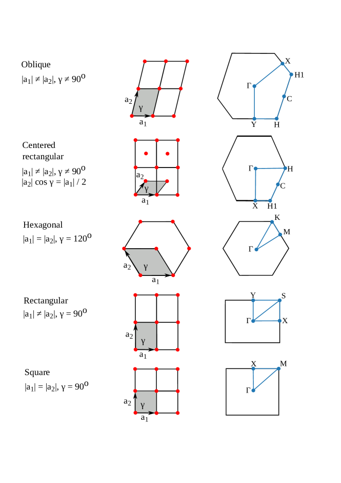
2.8 Band structures
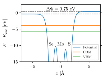
Electronic band structures are calculated along the high symmetry paths shown in Figure 8 for the five different types of 2D Bravais lattices. The band energies are computed within DFT using three different xc-functionals, namely PBE, HSE06, and GLLBSC. These single-particle approaches are complemented by many-body G0W0 calculations for materials with a finite gap and up to four atoms in the unit cell (currently around 250 materials). For all methods, SOC is included by non-selfconsistent diagonalisation in the full basis of Kohn-Sham eigenstates. Band energies always refer to the vacuum level defined as the asymptotic limit of the Hartree potential, see Figure 12. Below we outline the employed methodology while Section 3.2.1 provides an overview and comparison of the band energies obtained with the different methods.
2.8.1 PBE band structure
The electron density is determined self-consistently on a uniform -point grid of density 12.0/. From this density, the PBE band structure is computed non-selfconsistently at 400 -points distributed along the band path (see Figure 8). Examples of PBE band structures are shown in Figure 2.4.1 for the ferromagnetic metal VO2 and the semiconductor WS2 both in the MoS2 prototype structure. The expectation value of the out-of-plane spin component, , is evaluated for each spinorial wave function, , and is indicated by the color of the band. For materials with inversion symmetry, the SOC cannot induce band splitting, meaning that is ill-defined and no color coding is used. The band structure without SOC is indicated by a dashed grey line. We have compared our PBE+SOC band gaps of 29 different monolayers with those obtained with the VASP code in Ref. 42 and find a mean absolute deviation of 0.041 eV.
![[Uncaptioned image]](/html/1806.03173/assets/x8.png)
![[Uncaptioned image]](/html/1806.03173/assets/x9.png)
![[Uncaptioned image]](/html/1806.03173/assets/x10.png)
2.8.2 HSE band structure
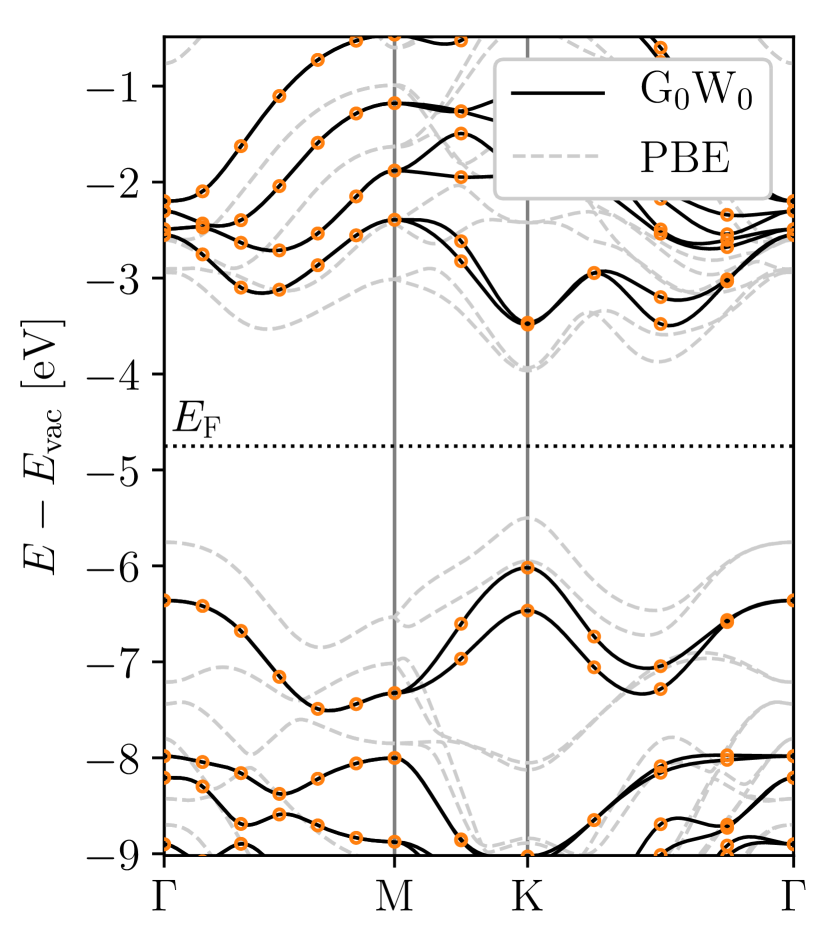
The band structure is calculated non-selfconsistently using the range-separated hybrid functional HSE06100 on top of a PBE calculation with -point density 12.0/ and 800 eV plane wave cutoff. We have checked for selected systems that the HSE band structure is well converged with these settings. The energies along the band path are obtained by spline interpolation from the uniform -point grid. As an example, the HSE band structure of WS2 is shown in the left panel of Figure 10 (black line) together with the PBE band structure (grey dashed). The PBE band gap increases from 1.52 eV to 2.05 eV with the HSE06 functional in good agreement with earlier work reporting band gaps of 1.50 eV (PBE) and 1.90 eV (HSE)101 and 1.55 eV (PBE) and 1.98 eV (HSE)102, respectively. A more systematic comparison of our results with the HSE+SOC band gaps obtained with the VASP code in Ref. 42 for 29 monolayers yield a mean absolute deviation of 0.14 eV. We suspect this small but non-zero deviation is due to differences in the employed PAW potentials and the non-selfconsistent treatment of the HSE in our calculations.
2.8.3 GLLBSC fundamental gap
For materials with a finite PBE band gap, the fundamental gap (i.e. the difference between the ionisation potential and electron affinity) also sometimes referred to as the quasiparticle gap, is calculated self-consistently using the GLLBSC103 xc-functional with a Monkhorst-Pack -point grid of density 12.0/. The GLLBSC is an orbital-dependent exact exchange-based functional, which evaluates the fundamental gap as the sum of the Kohn-Sham gap and the xc-derivative discontinuity, . The method has been shown to yield excellent quasiparticle band gaps at very low computational cost for both bulk103, 104 and 2D semiconductors36.
In the exact Kohn-Sham theory, should equal the exact ionisation potential and thus should be used to correct only the conduction band energies105. Unfortunately, we have found that in practice this procedure leads to up-shifted band energies (compared with the presumably more accurate G0W0 results, see Figure 20). Consequently, we store only the fundamental gap and in the database. However, as will be shown in Section 3.2.1 the center of the gap is in fact reasonably well described by PBE suggesting that efficient and fairly accurate predictions of the absolute band edge energies can be obtained by a symmetric GLLBSC correction of the PBE band edges.
2.8.4 GW band structure
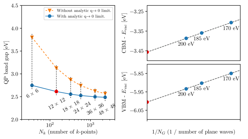
For materials with finite PBE band gap the quasiparticle (QP) band structure is calculated using the G0W0 approximation on top of PBE following our earlier work 106, 107. Currently, this resource demanding step is performed only for materials with up to four atoms in the unit cell. The number of plane waves and the number of unoccupied bands included in the calculation of the non-interacting density response function and the GW self-energy are always set equal. The individual QP energies are extrapolated to the infinite basis set limit from calculations at plane wave cutoffs of 170, 185 and 200 eV, following the standard dependence108, 109, see Figure 11(right). The screened Coulomb interaction is represented on a non-linear real frequency grid ranging from 0 eV to 230 eV and includes around 250 frequency points. The exchange contribution to the self-energy is calculated using a Wigner-Seitz truncation scheme110 for a more efficient treatment of the long range part of the exchange potential. For the correlation part of the self-energy, a 2D truncation of the Coulomb interaction is used111, 112. We stress that the use of a truncated Coulomb interaction is essential to avoid unphysical screening from periodically repeated layers which otherwise leads to significant band gap reductions.
Importantly, the use of a truncated Coulomb interaction leads to much slower -point convergence because of the strong -dependence of the 2D dielectric function around . We alleviate this problem by using an analytical expression for the screened interaction when performing the BZ integral around 107. This allows us to obtain well converged results with a relatively low -point density of 5.0/ (corresponding to for MoS2). For example, with this setting the G0W0 band gap of MoS2 is converged to within 0.05 eV, see Figure 11(left). In comparison, standard BZ sampling with no special treatment of the limit, requires around -points to reach the same accuracy.
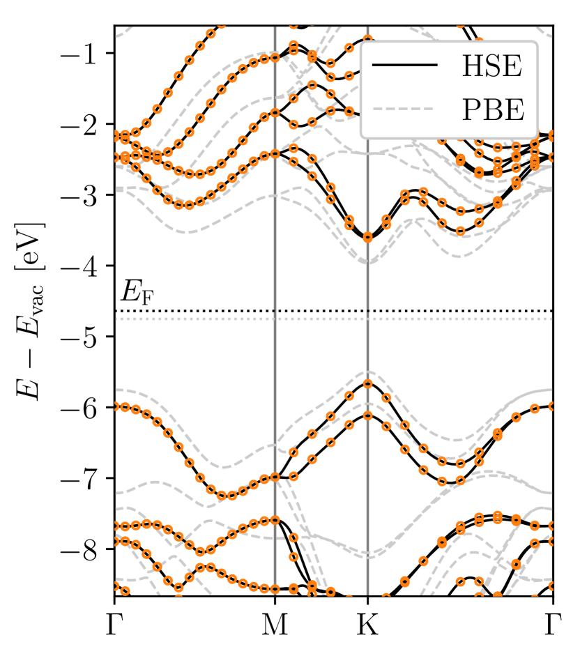
Figure 10 (right) shows the PBE and G0W0 band structures of WS2 (including SOC). The G0W0 self-energy opens the PBE band gap by 1.00 eV and the HSE gap by 0.47 eV, in good agreement with previous studies113. We note in passing that our previously published G0W0 band gaps for 51 monolayer TMDCs36 are in good agreement with the results obtained using the workflow described here. The mean absolute error between the two data sets is around 0.1 eV and can be ascribed to the use of PBE rather than LDA as starting point and the use of the analytical expression for around .
A detailed comparison of our results with previously published G0W0 data is not meaningful because of the rather large differences in the employed implementations/parameter settings. In particular, most reported calculations do not employ a truncated Coulomb interaction and thus suffer from spurious screening effects, which are then corrected for in different ways. Moreover, they differ in the amount of vacuum included the supercell, the employed -point grids and basis sets, the in-plane lattice constants, and the DFT starting points. For example, published values for the QP band gap of monolayer MoS2 vary from from 2.40 to 2.90 eV114, 115, 116, 117, 118, 119, 120, 121 (see Ref. 120 for a detailed overview). The rather large variation in published GW results for 2D materials is a result of the significant numerical complexity of such calculations and underlines the importance of establishing large and consistently produced benchmark data sets like the present.
For bulk materials, self-consistency in the Green’s function part of the self-energy, i.e. the GW0 method, has been shown to increase the G0W0 band gaps and improve the agreement with experiments122. The trend of band gap opening is also observed for 2D materials107, 123, 121, 121, however, no systematic improvement with respect to experiments has been established123. For both bulk and 2D materials, the fully self-consistent GW self-energy systematically overestimates the band gap122, 123 due to the neglect of vertex corrections124, 123. In G0W0 the neglect of vertex corrections is partially compensated by the smaller band gap of the non-interacting Kohn-Sham Green’s function compared to the true interacting Green’s function. In this case, the vertex corrections affect mainly the absolute position of the bands relative to vacuum while the effect on the band gap is relatively minor123.
In Table 4 we compare calculated band gaps from C2DB with experimental band gaps for three monolayer TMDCs and phosphorene. The experimental data has been corrected for substrate interactions123, 125, but not for zero-point motion, which is expected to be small (). The G0W0 results are all within 0.2 eV of the experiments. A further (indirect) test of the G0W0 band gaps against experimental values is provided by the comparison of our BSE spectra against experimental photoluminescence data in Table 7, where we have used a G0W0 scissors operator. Finally, we stress that the employed PAW potentials are not norm-conserving, and this can lead to errors for bands with highly localised states (mainly 4 and 3 orbitals), as shown in Ref. 126. Inclusion of vertex corrections and use of norm conserving potentials will be the focus of future work on the C2DB.
| Band gap (eV) | |||||
|---|---|---|---|---|---|
| Material | PBE | HSE06 | GLLBSC | G0W0 | Experiment |
| MoS2 | 1.58 | 2.09 | 2.21 | 2.53 | 2.50127 |
| MoSe2 | 1.32 | 1.80 | 1.88 | 2.12 | 2.31128 |
| WS2 | 1.53 | 2.05 | 2.16 | 2.53 | 2.72129 |
| P (phosphorene) | 0.90 | 1.51 | 1.75 | 2.03 | 2.20125 |
| MAD w.r.t. experiment | 1.10 | 0.57 | 0.43 | 0.15 | - |
2.9 Band extrema
For materials with a finite band gap, the positions of the valence band maximum (VBM) and conduction band minimum (CBM) within the BZ are identified together with their energies relative to the vacuum level. The latter is defined as the asymptotic value of the electrostatic potential, see Figure 12. The PBE electrostatic potential is used to define the vacuum level in the non-selfconsistent HSE and G0W0 calculations. For materials with an out-of-plane dipole moment, a dipole correction is applied during the selfconsistent DFT calculation, and the vacuum level is defined as the average of the asymptotic electrostatic potentials on the two sides of the structure. The PBE vacuum level shift is also stored in the database.
2.10 Fermi surface
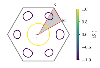
The Fermi surface is calculated using the PBE xc-functional including SOC for all metallic compounds in the database. Based on a ground state calculation with a -point density of at least 20/Å-1, the eigenvalues are interpolated with quadratic splines and plotted within the first BZ. Figure 13 (left) shows an example of the Fermi surface for VO2-MoS2 with color code indicating the out-of-plane spin projection . The band structure refers to the ferromagnetic ground state of VO2-MoS2, which has a magnetic moment of 0.70 per unit cell, characterised by alternating spin-polarised lobes with .
2.11 Effective masses
For materials with a finite PBE gap, the effective electron and hole masses are calculated from the PBE eigenvalues; initially these are calculated on an ultrafine -point mesh of density uniformly distributed inside a circle of radius 0.015 centered at the VBM and CBM, respectively. The radius is chosen to be safely above the noise level of the calculated eigenvalues but still within the harmonic regime; it corresponds to a spread of eigenvalues of about 1 meV within the circle for an effective mass of 1 . For each band within an energy window of 100 meV above/below the CBM/VBM, the band curvature is obtained by fitting a third order polynomial. Even though the masses represent the second derivative of the band energies, we have found that the inclusion of 3rd order terms stabilises the fitting procedure and yields masses that are less sensitive to the details of the employed -point grids. For each band the mass tensor is diagonalised to yield heavy and light masses in case of anisotropic band curvatures. The masses (in two directions) and the energetic splitting of all bands within 100 meV of the band extremum are calculated both with and without SOC and stored in the database. Other approaches exist for calculating effective masses, such as perturbation theory (see e.g. 130 and references therein); the present scheme was chosen for its simplicity and ease of application to a wide range of different materials.
In addition to the effective masses at the VBM and CBM, the exciton reduced mass is calculated by applying the above procedure to the direct valence-conduction band transition energies, . For direct band gap materials the exciton reduced mass is related to the electron and hole masses by , but in the more typical case of indirect band gaps, this relation does not hold.
As an example, Figure 14 shows a zoom of the band structure of SnS-GeSe around the VBM and CBM (upper and lower panels). The second order fits to the band energies (extracted from the fitted 3rd order polynomial) are shown by red dashed lines. It can be seen that both the conduction and valence bands are anisotropic leading to a heavy and light mass direction (left and right panels, respectively). The valence band is split by the SOC resulting in two bands separated by meV and with slightly different curvatures. The conduction band exhibits a non-trivial band splitting in one of the two directions. The peculiar band splitting is due to a Rashba effect arising from the combination of spin-orbit coupling and the finite perpendicular electric field created by the permanent dipole of the SnS structure where Sn and S atoms are displaced in the out of plane direction leading to a sizable vacuum level difference of 1.13 eV, see Figure 12.
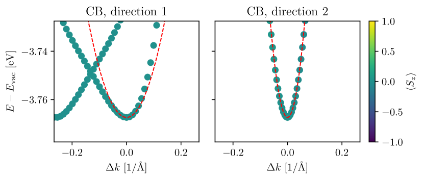
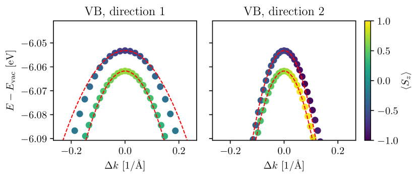
Table 5 shows a comparison between selected effective masses from the C2DB and previously published data also obtained with the PBE xc-correlation functional and including SOC. Overall, the agreement is very satisfactory.
| Electron mass () | Hole mass () | ||||
|---|---|---|---|---|---|
| Material | -point | C2DB | Literature | C2DB | Literature |
| MoS2 | K | 0.42 | 0.44130 | 0.53 | 0.54130 |
| WSe2 | K | 0.46 | 0.40130 | 0.35 | 0.36130 |
| Phosphorene (zig-zag) | 1.24 | 1.2496 | 6.56 | 6.4896 | |
| Phosphorene (armchair) | 0.14 | 0.1396 | 0.13 | 0.1296 | |
| MAD | 0.02 | - | 0.03 | - | |
2.12 Work function
For metallic compounds, the work function is obtained as the difference between the Fermi energy and the asymptotic value of the electrostatic potential in the vacuum region, see Figure 12. The work function is determined for both PBE and HSE band structures (both including SOC) on a uniform -point grid of density 12.0/Å-1. Since the SOC is evaluated non-selfconsistently, the Fermi energy is adjusted afterwards based on a charge neutrality condition.
2.13 Deformation potentials
For semiconductors, the deformation potentials quantify the shift in band edge energies (VBM or CBM) upon a linear deformation of the lattice. The uniaxial absolute deformation potential along axis () is defined as 131, 132
| (7) |
where is the energy shift upon strain and are the strains in the -directions.
The deformation potentials are important physical quantities as they provide an estimate of the strength of the (acoustic) electron-phonon interaction, see Section 3.2.2. Moreover, they are obviously of interest in the context of strain-engineering of band gaps and they can be used to can be used to infer an error bar on the band gap or band edge positions due to a known or estimated error bar on the lattice constant.
The calculation of is based on a central difference approximation to the derivative. A strain of is applied separately in the and directions and the ions are allowed to relax while keeping the unit cell fixed. Calculations are performed with the PBE xc-functional, a plane wave cutoff of 800 eV, and a -point density of 12/Å-1.
The change in band energy, , is measured relative to the vacuum level. In cases with nearly degenerate bands, care must be taken to track the correct bands as different bands might cross under strain. In this case, we use the expectation value to follow the correct band under strain. Figure 15 shows how the band structure of MoS2 changes as a function of strain. Both the VBM and the CBM shift down (relative to the vacuum level) when tensile strain is applied in the direction, but the conduction band shows a much larger shift, leading to an effective band gap closing under tensile strain.
2.14 Plasma frequencies
The dielectric response of a 2D material is described by its 2D polarisability, (see Section 2.15 for a general introduction of this quantity). For metals, it can be separated into contributions from intraband and interband transitions, i.e. . We have found that local field effects (LFEs) are negligible for the intraband component, which consequently can be treated separately and evaluated as an integral over the Fermi surface. Specifically, this leads to the Drude expression for the polarisability in the long wave length limit where is the 2D plasma frequency, which in atomic units is given by
| (8) |
where is a velocity matrix element (with the electron mass), is the polarisation direction, denote spin, band and momentum indices, and is the supercell area. The 2D plasma frequency is related to the conventional 3D plasma frequency by where is the supercell height.
The plasma frequency defined above determines the intraband response of the 2D metal to external fields. In particular, it determines the dispersion relation of plasmon excitations in the metal. The latter are defined by the condition , where is the plasmon wave vector. Neglecting interband transitions (the effect of which is considered in Section 3.2.4), the 2D plasmon dispersion relation becomes
| (9) |
The plasma frequencies, , for polarisation in the and directions, respectively, are calculated for all metals in the C2DB using the tetrahedral method99 to interpolate matrix elements and eigenvalues based on a PBE band structure calculation including SOC and with a -point density of .
2.15 Electronic polarisability
The polarisability tensor is defined by
| (10) |
where is the ’th component of the induced polarisation averaged over a unit cell and Ej is the ’th component of the macroscopic electric field. Using that one observes that , where is the dielectric function. In contrast to the dielectric function, whose definition for a 2D material is not straightforward120, the polarisability allows for a natural generalisation to 2D by considering the induced dipole moment per unit area,
| (11) |
Since the is a full unit cell average and is integrated in the direction orthogonal to the slab, we have and , where is the length of the unit cell in the direction orthogonal to the slab.
In the following, we focus on the longitudinal components of the polarisability and dielectric tensors, which are simply denoted by and . These are related to the density-density response function, , via the relations
| (12) | ||||
| (13) |
where is the Coulomb interaction and
| (14) |
where is the supercell with volume . The response function, , satisfies the Dyson equation134 where is the irreducible density-density response function. In the random phase approximation (RPA) is replaced by the non-interacting response function, , whose plane wave representation is given by135, 136
| (15) |
where are reciprocal lattice vectors and is the crystal volume.
For all materials in the database, we calculate the polarisability within the RPA for both in-plane and out-of-plane polarisation in the optical limit . For metals, the interband contribution to the polarisability is obtained from Eq. (15) while the intraband contribution is treated separately as described in Section 2.14. The single-particle eigenvalues and eigenstates used in Eq. 15 are calculated with PBE, a -point density of (corresponding to a -point grid of for MoS2 and for graphene), and 800 eV plane wave cutoff. The Dyson equation is solved using a truncated Coulomb potential137, 138 to avoid spurious interactions from neighboring images. We use the tetrahedron method to interpolate the eigenvalues and eigenstates and a peak broadening of meV. Local field effects are accounted for by including -vectors up to 50 eV. For the band summation we include 5 times as many unoccupied bands as occupied bands, which roughly corresponds to an energy cutoff of 50 eV. The calculations are performed without spin-orbit coupling.
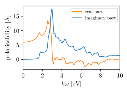
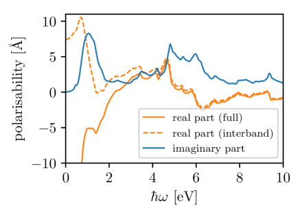
In Figure 16 we show the real and imaginary part of for the semiconductor MoS2. The PBE band gap of this material is 1.6 eV and we see the onset of dissipation at that energy. We also see that the initial structure of is a constant, which is exactly what would be expected from the density of states in a 2D material with parabolic dispersion. Finally, we note that the static polarisability , which can easily be read off the figure. The polarisability is also shown for the metallic 1T-NbS2 where we display the real part with and without the intraband Drude contribution .
2.16 Optical absorbance
The power absorbed by a 2D material under illumination of a monochromatic light field with polarisation is quantified by the dimensionless absorbance:
| (16) |
where is the speed of light. In Section (2.15) we gave a prescription for evaluating in the RPA. However, absorption spectra of 2D semiconductors often display pronounced excitonic effects, which are not captured by the RPA. The Bethe-Salpeter equation (BSE) is a well-known method capable of describing excitonic effects and has been shown to provide good agreement with experimental absorption spectra for a wide range of materials.139
For materials with finite band gap and up to four atoms per unit cell, we have calculated the RPA and the BSE absorption spectra for electric fields polarised parallel and perpendicular to the layers. The calculations are performed on top of PBE eigenstates and eigenvalues with spin-orbit coupling included and all unoccupied band energies shifted by a constant in order to reproduce the G0W0 quasiparticle gap (the scissors operator method). If the G0W0 gap is not available we use the GLLBSC gap for non-magnetic materials and the HSE gap for magnetic materials (since GLLBSC is not implemented in GPAW for spin-polarised systems). The screened interaction entering the BSE Hamiltonian is calculated within the RPA using a non-interacting response function evaluated from Eq. (15) with local field effects (i.e. -vectors) included up to 50 eV and 5 times as many unoccupied bands as occupied bands for the sum over states. We apply a peak broadening of meV and use a truncated Coulomb interaction. The BSE Hamiltonian is constructed from the four highest occupied and four lowest unoccupied bands on a -point grid of density of , and is diagonalised within the Tamm-Dancoff approximation. We note that the Tamm-Dancoff approximation has been found to be very accurate for bulk semiconductors140. For monolayer MoS2 we have checked that it reproduces the full solution of the BSE, but its general validity for 2D materials, in particular those with small band gaps, should be more thoroughly tested.
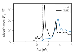
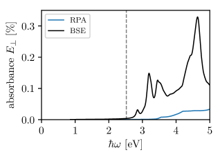
In Figure 17 we show the optical absorption spectrum of MoS2 obtained with the electric field polarised parallel and perpendicular to the layer, respectively. Both RPA and BSE spectra are shown (the in-plane RPA absorbance equals the imaginary part of the RPA polarisability, see Figure 16(left), apart from the factor and the scissors operator shift). The low energy part of the in-plane BSE spectrum is dominated by a double exciton peak (the so-called A and B excitons) and is in excellent agreement with experiments.141
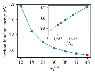
In general, calculations of electronic excitations of 2D materials converge rather slowly with respect to -points due to the non-analytic behavior of the dielectric function in the vicinity of .142, 143, 144 In Figure 18 we show the -point dependence of the binding energy of the A exciton in MoS2 obtained as the difference between the direct band gap and the position of the first peak in Figure 17. We observe a strong overestimation of the exciton binding energy at small -point samplings, which converges slowly to a value of eV at large -point samplings. For -points, corresponding to the -point sampling used for the BSE calculations in the database, the exciton binding energy is 0.53 eV, whereas a extrapolation to infinite -point sampling gives 0.47 eV (see inset in Figure 18). In general, the exciton binding energy decreases with increasing -point sampling, and thus the exciton binding energies reported in the C2DB might be slightly overestimated. However, since G0W0 band gaps also decrease when the -point sampling is increased (see Figure 11) the two errors tend to cancel such that the absolute position of the absorption peak from BSE-G0W0 converges faster than the band gap or exciton binding energy alone.
The BSE-G0W0 method has previously been shown to provide good agreement with experimental photoluminescence and absorption measurements on 2D semiconductors. In Table 7 we show that our calculated position of the first excitonic peak agree well with experimental observations for four different TMDCs and phosphorene. Experimentally, the monolayers are typically supported by a substrate, which may alter the screening of excitons. However the resulting decrease in exciton binding energies is largely cancelled by a reduced quasiparticle gap such that the positions of the excitons are only slightly red-shifted as compared with the case of pristine monolayers145.
| Energy of the first bright exciton (eV) | ||
| Material | BSE@PBE-G0W0 | Experiment |
| MoS2 | 2.00 | 1.83146, 1.86147, 1.87148 |
| MoSe2 | 1.62 | 1.57146, 1.57149, 1.58150 |
| WS2 | 2.07 | 1.96147, 2.02150 |
| WSe2 | 1.71 | 1.64148, 1.66149 |
| P (phosphorene) | 1.45 | 1.45151, 1.75152 |
| MAD w.r.t. experiment | 0.066 | - |
3 Database overview
Having described the computational workflow, we now turn to the content of the database itself. We first present a statistical overview of all the materials in the C2DB (i.e. without applying any stability filtering) by displaying their distribution over crystal structure prototypes and their basic properties. We also provide a short list with some of the most stable materials, which to our knowledge have not been previously studied. Next, the predicted stability of the total set of materials is discussed and visualised in terms of the descriptors for thermodynamic and dynamic stability introduced in Section 2.4.1. In Section 3.2 we analyse selected properties in greater detail focusing on band gaps and band alignment, effective masses and mobility, magnetic properties, plasmons, and excitons. Throughout the sections we explore general trends and correlations in the data and identify several promising materials with interesting physical properties.
3.1 Materials
In Table 8 we list the major classes of materials currently included in the database. The materials are grouped according to their prototype, see Section 2.2.2. For each prototype we list the corresponding space group, the total number of materials, and the number of materials satisfying a range of different conditions. The atomic structure of some of the different prototypes were shown in Figure 4. The vast majority of the 2D materials that have been experimentally synthesised in monolayer form are contained in the C2DB (the 55 materials in Figure 7 in addition to seven metal-organic perovskites). These materials are marked in the database and a literature reference is provided. Additionally, 80 of the monolayers in the C2DB could potentially be exfoliated from experimentally known layered bulk structures17, 16, 18, 19. These materials are also marked and the ID of the bulk compound in the relevant experimental crystal structure database is provided.
| Number of materials | ||||||||
| Prototype | Symmetry | Total | Direct gap | High stability | NM | FM | AFM | |
| C | P6/mmm | 4 | 4 | 3 | 1 | 4 | 0 | 0 |
| CH | Pm1 | 8 | 7 | 6 | 1 | 8 | 0 | 0 |
| CH2Si | P3m1 | 2 | 2 | 2 | 1 | 2 | 0 | 0 |
| BN | Pm2 | 10 | 9 | 5 | 1 | 10 | 0 | 0 |
| GaS | Pm2 | 125 | 34 | 95 | 8 | 100 | 18 | 7 |
| FeSe | P4/nmm | 103 | 13 | 90 | 26 | 74 | 18 | 11 |
| GeSe | P3m1 | 20 | 19 | 5 | 6 | 20 | 0 | 0 |
| PbSe | P4/mmm | 44 | 6 | 38 | 1 | 33 | 8 | 3 |
| P | Pmna | 9 | 9 | 0 | 1 | 9 | 0 | 0 |
| MoS2 | Pm2 | 241 | 85 | 176 | 53 | 156 | 85 | 0 |
| CdI2 | Pm1 | 315 | 95 | 231 | 90 | 218 | 80 | 17 |
| WTe2 | P21/m | 75 | 29 | 48 | 34 | 57 | 13 | 5 |
| FeOCl | Pmmn | 443 | 92 | 385 | 65 | 328 | 63 | 52 |
| MoSSe | P3m1 | 9 | 6 | 6 | 5 | 8 | 1 | 0 |
| C3N | P6/mmm | 25 | 1 | 24 | 0 | 25 | 0 | 0 |
| YBr3 | P6/mmm | 57 | 11 | 51 | 0 | 21 | 24 | 12 |
| TiCl3 | P2m | 69 | 35 | 51 | 2 | 32 | 23 | 14 |
| BiI3 | Pm1 | 123 | 69 | 66 | 15 | 48 | 54 | 21 |
| TiS3 | Pmmn | 34 | 8 | 28 | 5 | 31 | 2 | 1 |
| MnTe3 | P21/m | 29 | 3 | 27 | 1 | 22 | 4 | 3 |
| Cr3WS8 | Pmm2 | 35 | 34 | 18 | 8 | 35 | 0 | 0 |
| CrWS4 | Pmm2 | 18 | 17 | 7 | 8 | 18 | 0 | 0 |
| Ti2CO2 | Pm1 | 28 | 8 | 20 | 12 | 19 | 6 | 3 |
| Ti2CH2O2 | Pm1 | 13 | 3 | 12 | 3 | 10 | 2 | 1 |
| Ti3C2 | Pm2 | 12 | 0 | 12 | 0 | 7 | 5 | 0 |
| Ti3C2O2 | Pm2 | 26 | 0 | 26 | 0 | 20 | 6 | 0 |
| Ti3C2H2O2 | Pm2 | 14 | 0 | 14 | 0 | 10 | 4 | 0 |
| PbA2I4 | P1 | 27 | 27 | 27 | 0 | 27 | 0 | 0 |
| Sum | 1918 | 626 | 151 | 347 | 1352 | 416 | 150 | |
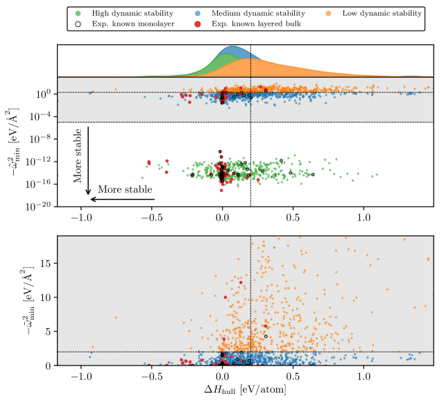
To illustrate how all the materials are distributed in terms of stability, we show the energy above the convex hull plotted against in Figure 19. It can be seen that the structures naturally sort themselves into two clusters according to the dynamic stability. The points have been colored according to the three levels for dynamic stability introduced in section 2.4. The lower panel shows the distribution of the materials in the grey region on a linear scale. While most of the experimentally known materials (red and black dots) have high dynamic stability, a significant part of them fall into the medium stability category. The marginal distributions on the plot show that the more dynamically stable materials are also more thermodynamically stable. The mean energy above the convex hull is 0.12 eV for the materials with high dynamical stability, while it is 0.25 eV for the others.
In Table 9 we show the key properties of a selected set of stable materials, distributed across a variety of different crystal structure prototypes. To our knowledge, these materials are not experimentally known, and they are therefore promising candidates further study and experimental synthesis.
| Prototype | Formula | Magnetic state | (eV) | (eV) | (eV) | PBE gap (eV) | Direct gap |
|---|---|---|---|---|---|---|---|
| BiI3 | VI3 | FM | 5.3 | ||||
| CoCl3 | NM | 1.13 | No | ||||
| CoBr3 | NM | 0.96 | No | ||||
| CoI3 | NM | 0.53 | No | ||||
| CdI2 | FeO2 | FM | 7.31 | ||||
| MnSe2 | FM | 5.09 | |||||
| MnS2 | FM | 5.74 | |||||
| PdO2 | NM | 1.38 | No | ||||
| CaBr2 | NM | 4.86 | No | ||||
| FeOCl | RhClO | NM | 5.49 | ||||
| NiClO | AFM | 6.32 | |||||
| NiBrO | AFM | 5.78 | |||||
| ScIS | NM | 1.66 | Yes | ||||
| FeSe | CoSe | FM | 0.02 | 4.22 | |||
| RuS | NM | 0.05 | 4.72 | ||||
| MnSe | AFM | 0.90 | No | ||||
| MnS | AFM | 0.78 | No | ||||
| GaS | AlSe | NM | 2.00 | No | |||
| AlS | NM | 0.00 | 2.09 | No | |||
| GeSe | GeSe | NM | 0.04 | 2.22 | No | ||
| GeS | NM | 0.05 | 2.45 | No | |||
| GeTe | NM | 0.09 | 1.47 | No | |||
| SnSe | NM | 0.10 | 2.15 | No | |||
| MoS2 | VS2 | FM | 5.95 | ||||
| ScBr2 | FM | 0.16 | No | ||||
| YBr2 | FM | 0.34 | No | ||||
| FeCl2 | FM | 0.35 | Yes | ||||
| TiBr2 | NM | 0.76 | No | ||||
| ZrBr2 | NM | 0.83 | No | ||||
| Ti2CO2 | Zr2CF2 | NM | 3.92 | ||||
| Hf2CF2 | NM | 0.03 | 3.62 | ||||
| Y2CF2 | NM | 1.12 | No | ||||
| WTe2 | NbI2 | NM | 0.04 | 3.01 | |||
| HfBr2 | NM | 0.85 | No | ||||
| OsSe2 | NM | 0.00 | 0.57 | No |
3.2 Properties: Example applications
In the following sections we present a series of case studies focusing on different properties of 2D materials including band gaps and band alignment, effective masses and mobility, magnetic order, plasmons and excitons. The purpose is not to provide an in-depth nor material specific analysis, but rather to explore trends and correlations in the data and showcase some potential applications of the C2DB. Along the way, we report some of the novel candidate materials revealed by this analysis, which could be interesting to explore closer in the future.
3.2.1 Band gaps and band alignment
The band gaps and band edge positions of all semiconductors and insulators in the C2DB have been calculated with the PBE, HSE06, and GLLBSC xc-functionals while G0W0 calculations have been performed for the 250 simplest materials. The relatively large size of these datasets and the high degree of consistency in the way they are generated (all calculations performed with the same code using same PAW potentials and basis set etc.) provide a unique opportunity to benchmark the performance of the different xc-functionals against the more accurate G0W0 method.
| PBE | HSE06 | GLLBSC | |
|---|---|---|---|
| MAD w.r.t. G0W0 (band gap) | 1.49 | 0.82 | 0.38 |
| MAD w.r.t. G0W0 (gap center) | 0.37 | 0.32 | 0.76 |
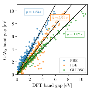
Figure 20 compares the size and center of the band gaps obtained with the density functionals to the G0W0 results. Relative to G0W0 the PBE functional underestimates the gaps by 45%, i.e. on average the PBE values must be scaled by to reproduce the G0W0 results. The HSE06 band gaps are closer to G0W0 but are nevertheless systematically underestimated by more than 20%. On the other hand, GLLBSC shows very good performance with band gaps only 2% smaller than G0W0 on average. Table 10 shows the mean absolute deviations of the DFT methods relative to G0W0 . We note that although GLLBSC provides an excellent description of the G0W0 band gaps on average the spread is sizable with a mean absolute deviation of 0.4 eV.
We note a handful of outliers in Figure 20 with large HSE band gaps compared to PBE and G0W0 . For one of these, namely the ferromagnetic CoBr2-CdI2, we obtain the band gaps: 0.30 eV (PBE), 3.41 eV (HSE), and 0.91 eV (G0W0). For validation, we have performed GPAW and QuantumEspresso calculations with the norm-conserving HGH pseudopotentials and plane wave cutoff up to 1600 eV. The converged band gaps are 0.49 eV (GPAW-HGH-PBE), 0.51 eV (QE-HGH-PBE) and 3.69 eV (GPAW-HGH-HSE), 3.52 eV (QE-HGH-HSE), which are all in reasonable agreement with the C2DB results. It should be interesting to explore the reason for the anomalous behavior of the HSE band gap in these materials.
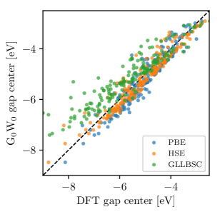
Compared to the band gaps, the gap centers predicted by PBE and HSE06 are in overall better agreement with the G0W0 results. This implies that, on average, the G0W0 correction of the DFT band energies is symmetric on the valence and conduction band. In contrast, the GLLBSC predicts less accurate results for the gap center. This suggests that an accurate and efficient prediction of absolute band energies is obtained by combining the GLLBSC band gap with the PBE band gap center.
Next, we consider the band alignment at the interface between different 2D materials. Assuming that the bands line up with a common vacuum level and neglecting hybridisation/charge transfer at the interface, the band alignment is directly given by the VBM and CBM positions relative to vacuum.
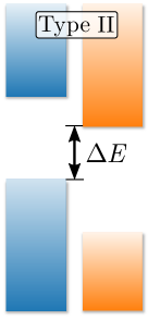
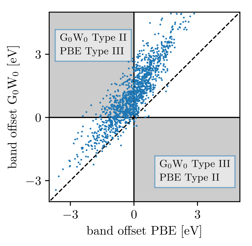
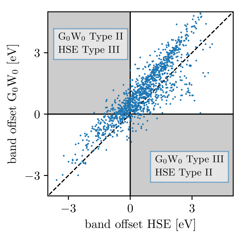
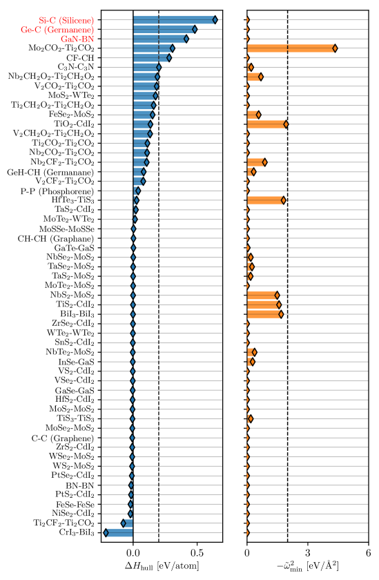
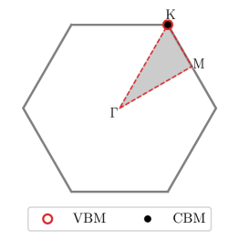
We focus on pairs of 2D semiconductors for which the G0W0 band alignment is either Type II () or Type III (), see Figure 21(left). Out of approximately 10000 bilayers predicted to have Type II band alignment by G0W0 , the PBE and HSE06 functionals predict qualitatively wrong band alignment (i.e. Type III) in 44% and 21% cases, respectively (grey shaded areas). In particular, PBE shows a sizable and systematic underestimation of as a direct consequence of the underestimation of the band gaps in both monolayers.
3.2.2 Effective masses and mobilities
The carrier mobility relates the drift velocity of electrons or holes to the strength of an applied electric field and is among the most important parameters for a semiconductor material. In general, the mobility is a sample specific property which is highly dependent on the sample purity and geometry, and (for 2D materials) interactions with substrate or embedding layers. Here we consider the phonon-limited mobility, which can be considered as the intrinsic mobility of the material, i.e. the mobility that would be measured in the absence of any sample specific- or external scattering sources.
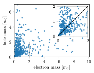
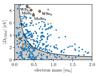
The effective masses of the charge carriers have been calculated both with and without SOC for semiconductors. Figure 22 shows the electron mass plotted against the hole mass. The data points are scattered, with no clear correlation between the electron and hole masses. Overall, the electron masses are generally slightly smaller than the hole masses. The mean electron mass is 0.9 , while the mean hole mass is 1.1 , and 80% of the electron masses are below while the fraction is only 65% for the holes. This is not too surprising, since, on average, the energetically lower valence band states are expected to be more localised and thus less dispersive than the conduction band states.
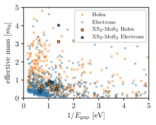
The right panel of Figure 22 shows the effective mass for electrons and holes plotted as a function of the inverse band gap. It can be seen that there is no clear correlation between the two quantities, which is confirmed by calculating the cross-correlation coefficient: for both electrons and holes it is less than 0.02. This provides empirical evidence against the linear relation between effective masses and inverse band gaps derived from perturbation theory. The relation is based on the assumption that the perturbative expansion is dominated by the conduction and valence band and that the momentum matrix element between these states, , does not vary too much as function of the considered parameter (here the type of material). These assumptions clearly do not hold across a large set of different semiconductors. If we focus on a specific class of materials, e.g. sulfides in the MoS2 structure indicated by the highlighted symbols, we see a slightly improved trend but still with significant fluctuations.
If one assumes energetically isolated and parabolic bands, the intrinsic mobility limited only by scattering on acoustic phonons can be estimated from the Takagi formula 153,
| (17) |
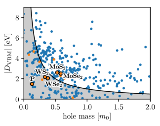
Here refers to the transport direction, is the mass density, is the speed of sound in the material, is the carrier mass, is the equivalent isotropic density-of-state mass defined as , and is the deformation potential. We stress that the simple Takagi formula is only valid for temperatures high enough that the acoustic phonon population can be approximated by the Rayleigh-Jeans law, , but low enough that scattering on optical phonons can be neglected.
For the semiconductors in the C2DB we have found that the denominator of Equation (17) varies more than the numerator. Consequently, a small product of deformation potential and effective mass is expected to correlate with high mobility. Figure 23 shows the deformation potential plotted against the carrier mass for the valence and conduction bands, respectively. The shaded area corresponds, somewhat arbitrarily, to the region for which . The 2D semiconductors which have been synthesised in monolayer form are indicated with orange symbols while those which have been used in field effect transistors are labeled. Consistent with experimental findings, phosphorene (P) is predicted to be among the materials with the highest mobility for both electrons and holes.
Interestingly, a number of previously unknown 2D materials lie in this shaded region and could be candidates for high mobility 2D semiconductors. Table 11 lists a few selected materials with high intrinsic mobility according to Equation (17), which all have “high” overall stability (see Section 2.4.1). In the future, it will be interesting to explore the transport properties of these candidate materials in greater detail.
To give a sense of scale for the numbers in Table 11 to scale, we consider the well studied example of MoS2. For this material we obtain an electron mobility of 240 cm2V-1s-1 while a full ab-initio calculation found a phonon-limited mobility of 400 cm2V-1s-1 (in good agreement with experiments on hBN encapsulated MoS2154), with the acoustic phonon contribution corresponding to a mobility of 1000 cm2V-1s-1. Similarly, for the series MX2 (M = W, Mo, X = S, Se), we calculate room-temperature electron mobilities between 200 cm2V-1s-1 and 400 cm2V-1s-1, which are all within 50% of the ab-initio results155. Presumably, as in the case for MoS2, the good quantitative agreement is partly a result of error cancellation between an overestimated acoustic phonon scattering and the neglect of optical phonon scattering. Importantly, however, the relative ordering of the mobilities of the four MX2 monolayers is correctly predicted by Equation (17) for all but one pair (MoS2 and WSe2) out of the six pairs. These results illustrate that Equation (17) should only be used for ”order of magnitude” estimates of the mobility whereas relative comparisons of mobilities in different materials are probably reliable.
| Carrier | Formula | Prototype | PBE gap (eV) | (cm2V-1s-1) | () | |
|---|---|---|---|---|---|---|
| Holes | PbS2 | MoS2 | 1.39 | 30000 | 0.62 | 1.4 |
| OsO2 | WTe2 | 0.17 | 23000 | 0.23 | 3.0 | |
| ZrCl2 | MoS2 | 0.98 | 12000 | 0.43 | 1.1 | |
| WSSe | MoSSe | 1.40 | 5500 | 0.37 | 1.0 | |
| Electrons | PtTe2 | CdI2 | 0.30 | 9600 | 0.17 | 1.3 |
| GaO | GaS | 1.56 | 7200 | 0.32 | 1.0 | |
| NiS2 | CdI2 | 0.58 | 6000 | 0.29 | 1.5 | |
| RuTe2 | WTe2 | 0.64 | 4600 | 1.55 | 8.5 |
3.2.3 Magnetic properties
Recently, a single layer of CrI3 was reported to exhibit ferromagnetic order with a Curie temperature of 45 K.12 This comprises the first example of a pure 2D material exhibiting magnetic order and there is currently an intense search for new 2D materials with magnetic order persisting above room temperature.156, 157, 158
For 2D materials, magnetic order will only persist at finite temperatures in the presence of magnetic anisotropy (MA). Indeed, by virtue of the Mermin-Wagner theorem, magnetic order is impossible in 2D unless the rotational symmetry of the spins is broken159. A finite MA with an out of plane easy axis breaks the assumption behind the Mermin-Wagner theorem and makes magnetic order possible at finite temperature. The critical temperature for magnetic order in 2D materials will thus have a strong dependence on the anisotropy.
The MA originates from spin-orbit coupling and is here defined as the energy difference between in-plane and out-of-plane orientation of the magnetic moments, see Eq. (4). With our definition, a negative MA corresponds to an out-of-plane easy axis. We note that most of the materials in the C2DB are nearly isotropic in-plane. Consequently, if the easy axis lies in the plane, the spins will exhibit an approximate in-plane rotational symmetry, which prohibits magnetic order at finite temperatures. Since spin-orbit coupling becomes large for heavy elements, we generally expect to find larger MA for materials containing heavier elements. In general the magnitude of the MA is small. For example, for monolayer CrI3 with a Curie temperature of 45 K12 we find a MA of meV per Cr atom in agreement with previous calculations160. Although small, the MA is, however, crucial for magnetic order to emerge at finite temperature.
In Figure 24 we show the magnitude of the magnetic anisotropy (red triangles) and the magnetic moment per metal atom (blue triangles) averaged over all materials with a given chemical composition. The plot is based on data for around 1200 materials in the medium to high stability categories (see Table 2.4.1) out of which around 350 are magnetic. It is interesting to note that while the magnetic moment is mainly determined by the metal atom, the MA depends strongly on the non-metal atom. For example, the halides (Cl, Br, I) generally exhibit much larger MAs than the chalcogenides (S, Se, Te). Overall, iodine (I) stands out as the most significant element for a large MA while the metals Cr, Mn, Fe and Co are the most important elements for a large magnetic moment. Since the MA is driven by spin-orbit coupling (SOC) and the spin is mainly located on the metal atom, one would expect a large MA to correlate with a heavy metal atom. However, it is clear from the figure that it is not essential that the spin-carrying metal atom should also host the large SOC. For example, we find large MA for several metal-iodides despite of the relatively weak SOC on the metals. This shows that the MA is governed by a rather complex interplay between the spins, orbital hybridisation and crystal field.
A selection of materials predicted to have high overall stability (see Section 2.4.1) and high out-of-plane magnetic anisotropy ( meV/magnetic atom) is listed in Tab. 12. We find several semiconductors with anisotropies comparable to CrI3 and several metals with even higher values. Looking also at materials with medium stability, we find semiconductors with anisotropies up to 2 meV. It is likely that some of these materials will have Curie temperatures similar to, or even higher than, CrI3.
| Formula | Prototype | Magnetic moment () | PBE gap (eV) | MA (meV/atom) | Magnetic state | (eV/atom) |
|---|---|---|---|---|---|---|
| OsI3 | BiI3 | 0.9 | 0.0 | FM | 0.18 | |
| CrTe | FeSe | 2.6 | 0.0 | AFM | 0.15 | |
| FeCl3 | BiI3 | 1.0 | 0.01 | FM | ||
| FeTe | FeSe | 1.9 | 0.0 | FM | 0.08 | |
| MnTe2 | CdI2 | 2.7 | 0.0 | FM | ||
| FeBr3 | BiI3 | 1.0 | 0.04 | FM | ||
| CrI3 | BiI3 | 3.0 | 0.90 | FM | ||
| MnTe | FeSe | 3.8 | 0.69 | AFM | ||
| NiO | PbSe | 1.1 | 0.0 | FM | 0.05 | |
| FeBrO | FeOCl | 1.1 | 0.0 | FM | ||
| CrISe | FeOCl | 3.0 | 0.0 | FM | ||
| MnSe2 | CdI2 | 2.8 | 0.0 | FM | ||
| CrIS | FeOCl | 3.0 | 0.35 | FM | ||
| MnO2 | CdI2 | 3.0 | 1.13 | FM | 0.02 | |
| VCl3 | BiI3 | 2.0 | 0.0 | FM | ||
| MnSe | FeSe | 3.7 | 0.90 | AFM | ||
| CrSe | FeSe | 2.0 | 0.0 | AFM | 0.12 |
In addition to the MA, the critical temperature depends sensitively on the magnetic exchange couplings. We are presently developing a workflow for systematic calculation of exchange coupling constants, which will allow us to estimate the Curie temperature of all the magnetically ordered 2D materials. The database contains several 2D materials with anti-ferromagnetic order. As a note of caution, we mention that the magnetic interactions in AFM materials typically arise from the super-exchange mechanism, which is poorly described by PBE and requires a careful verification using a PBE+U scheme161.
3.2.4 Plasmons
The unique optical properties of 2D materials make them highly interesting as building blocks for nanophotonic applications162, 163. Many of these applications involve electron rich components which can capture, focus, and manipulate light via plasmons or plasmon-polaritons. Graphene sheets can host plasmons that are long lived, can be easily tuned via electrostatic or chemical doping, and can be used to confine light to extremely small volumes164. However, due to the limited charge carrier density achievable in graphene, its plasmons are limited to the mid-infrared regime. Here we show that some metallic monolayers support plasmons with significantly higher energies than graphene and could potentially push 2D plasmonics into the optical regime.
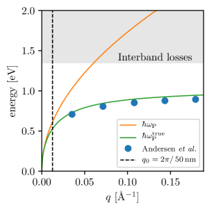
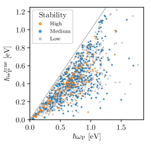
Figure 25 (left) shows the plasmon dispersion for monolayer NbS2 in the MoS2 crystal structure. The effect of interband transitions on the plasmon is significant as can be seen by comparison to the pure intraband plasmon (). The true plasmon energies are obtained from the poles of the (long wave length limit) dielectric function including the interband transitions, , yielding . For simplicity we ignore the frequency dependence of the interband polarisability, i.e. we set , which should be valid for small plasmon energies (far from the onset of interband transitions). The validity of this approximation is confirmed by comparing to the full ab initio calculations of Andersen et al. (blue dots) which include the full - and -dependence.165 The figure shows that interband screening generally reduces the plasmon energy and becomes increasingly important for larger .
Figure 25 (right) shows the in-plane averaged true plasmon energy of all metals in the C2DB plotted against the intraband plasmon energy at a fixed plasmon wavelength of nm (corresponding to at the dashed vertical line in the left panel). For comparison, the plasmon energy of freestanding graphene at this wavelength and for the highest achievable doping level ( eV relative to the Dirac point) is around 0.4 eV. The data points are colored according to the overall stability level as defined in Section 2.4.1. Table 13 shows a selection of the 2D metals with ”high” overall stability (see Section 2.4.1) and large plasmon frequencies. We briefly note the interesting band structures of the metals in the FeOCl prototype (not shown) which exhibits band gaps above or below the partially occupied metallic band(s), which is likely to lead to reduced losses in plasmonic applications.166 A detailed study of the plasmonic properties of the lead candidate materials will be published elsewhere. However, from Figure 25 (right) it is already clear that several of the 2D metals have plasmon energies around 1 eV at nm, which significantly exceeds the plasmon energies in highly doped graphene.
| Prototype | Formula | Magnetic state | [eV] | [Å] | [eVÅ] |
|---|---|---|---|---|---|
| TiS3 | TaSe3 | NM | 0.99 | 12.54 | 12.48 |
| FeOCl | PdClS | NM | 0.93 | 4.13 | 9.52 |
| FeOCl | NiClS | NM | 0.90 | 5.60 | 9.66 |
| CdI2 | TaS2 | NM | 0.82 | 5.59 | 8.79 |
| FeOCl | ZrIS | NM | 0.75 | 7.68 | 8.43 |
| CdI2 | NbS2 | NM | 0.73 | 8.2 | 8.42 |
| FeOCl | ZrClS | NM | 0.73 | 13.6 | 9.35 |
| TiS3 | TaS3 | NM | 0.73 | 34.22 | 12.44 |
| PbSe | NiO | FM | 0.72 | 2.9 | 7.16 |
3.2.5 Excitons
Two-dimensional materials generally exhibit pronounced many-body effects due to weak screening and strong quantum confinement. In particular, exciton binding energies in monolayers are typically an order of magnitude larger than in the corresponding layered bulk phase and it is absolutely crucial to include excitonic effects in order to reproduce experimental absorption spectra.
The electronic screening is characterised by the in-plane 2D polarisability, see Eq. (12). For a strictly 2D insulator, the screened Coulomb potential can be written as with and is the 2D Fourier transform of the Coulomb interaction. The -dependence of indicates that the screening is non-local, i.e. it cannot be represented by a -independent dielectric constant, and that Coulomb interactions tend to be weakly screened at large distances (small vectors).167, 168, 142 This is in sharp contrast to the case of 3D semiconductors/insulators where screening is most effective at large distances where its effect can be accounted for by a -independent dielectric constant. For a two-band model with isotropic parabolic bands, the excitons can be modeled by a 2D Hydrogen-like (Mott-Wannier) Hamiltonian where the Coulomb interaction is replaced by and the electron mass is replaced by a reduced excitonic mass derived from the curvature of conduction and valence bands. It has previously been shown that the excitonic Rydberg series of a 2D semiconductor can be accurately reproduced by this model if the dielectric constant, , is obtained by averaging over the extent of the exciton in reciprocal space169. For the lowest exciton (), the binding energy can then be expressed as
| (18) |
It has furthermore been demonstrated that this expression gives excellent agreement with a numerical solution of the Mott-Wannier model employing the full -dependent dielectric function, , for 51 transition metal dichalcogenides.169 We note that the previous calculations were based on LDA and we generally find that the PBE values for obtained in the present work are 10-20 % smaller compared with LDA.
In Figure 26, we compare the binding energy of the lowest exciton obtained from BSE-PBE with G0W0 scissors operator and the Mott-Wannier model Eq. (18), respectively. Results are shown for the 194 non-magnetic semiconductors out of the total set of materials for which BSE calculations have been performed. We focus on the optically active zero-momentum excitons and compute the exciton masses by evaluating the curvature of the band energies at the direct gap, see Section 2.11. For anisotropic materials we average the heavy and light exciton masses as well as the and components of the polarisability, , to generate input parameters for the isotropic model Eq. (18).
Although a clear correlation with the BSE results is observed, it is also evident that the Mott-Wannier model can produce significant errors. The mean absolute deviation between BSE and the model is eV for all materials and 0.20 eV for the subset of transition metal dichalcogenides (TMDCs). Furthermore, the Mott-Wannier model seems to overestimate for more strongly bound excitons while the opposite trend is seen for weakly bound excitons. As explained below these trends are a consequence of systematic errors in the Mott-Wannier model which can be traced to two distinct sources.
(i) Weak screening: If is small (on the order of 1 Å), the exciton becomes strongly localised and the orbital character of the states comprising the exciton plays a significant role. In general, the Mott-Wannier model tends to overestimate the exciton binding energy in this case as can be seen from the relatively large deviation of points with model binding energies eV in Figure 26. The overestimated binding energy results from the homogeneous electron and hole distributions implicitly assumed in the Mott-Wannier model. In reality, the short range variation of the electron and hole distributions is determined by the shape of the conduction and valence band states. In general these will differ leading to a reduced spatial overlap of the electron and hole and thus a lower Coulomb interaction. For example, SrCl2 in the CdI2 prototype ( Å) has a BSE binding energy of 2.1 eV and a model binding energy of 3.4 eV. From the PDOS of this material (see the C2DB webpage) it is evident that the electron and hole are mainly residing on the Sr and Cl atoms, respectively.
(ii) Breakdown of the parabolic band approximation: Materials with small band gaps often exhibit hyperbolic rather than parabolic band structures in the vicinity of the band gap. This typically happens in materials with small band gaps such as BSb in the BN prototype. In Figure 26 these materials can be identified as the cluster of points with model binding energies eV and BSE binding energies eV. A similar situation occurs if the conduction and valence bands flatten out away from the band gap region. In both of these cases, the excitons tend to be delocalised over a larger area in the Brillouin zone than predicted by the parabolic band approximation of the Mott-Wannier model. Typically, such delocalisation will result in larger binding energies than predicted by the model. For example, FeI2 in the CdI2 prototype exhibits shallow band minima in a ring around the -point and has a BSE binding energy of 1.1 eV and a model binding energy of 0.5 eV because the model assumes that the exciton will be located in the vicinity of the shallow minimum (and thus more delocalised in real space). A detailed inspection reveals that such break down of the parabolic band approximation is responsible for most of the cases where the model underestimates the binding energy.
Other sources of errors come from contributions to the exciton from higher/lower lying bands, i.e. break down of the two-band approximation, and anisotropic exciton masses not explicitly accounted for by Eq. (18).
Based on this comprehensive and unbiased assessment of the Mott-Wannier model, we conclude that while the model can be useful for understanding trends and qualitative properties of excitons, its quantitative accuracy is rather limited when applied to a broad set of materials without any parameter tuning. For quantitative estimates should not be too small (certainly not less than 2 Å) and the the validity of the effective mass approximation should be carefully checked by inspection of the band structure.
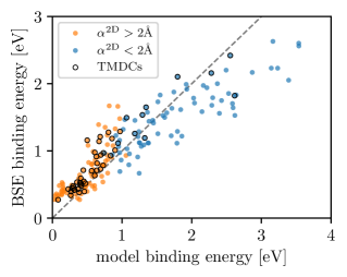
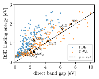
It has been argued that there should exist a robust and universal scaling between the exciton binding energy and the quasiparticle band gap of 2D semiconductors, namely .170 This scaling relation was deduced empirically based on BSE-GW calculations for around 20 monolayers and explained from Equation (18) and the relation from perturbation theory. Another work observed a similar trend171 but explained it from the dependence of the exciton effective mass expected from perturbation theory. Based on our results we can completely refute the latter explanation (see Figure 22(right)). In Figure 26(right) we show the exciton binding energy plotted versus the direct PBE and G0W0 band gaps, respectively. While there is a correlation, it is by no means as clear as found in Ref. 170.
4 Conclusions and Outlook
The C2DB is an open database with calculated properties of two-dimensional materials. It currently contains more than 1500 materials distributed over 32 different crystal structures. A variety of structural, elastic, thermodynamic, electronic, magnetic and optical properties are computed following a high-throughput, semi-automated workflow employing state of the art DFT and many-body methods. The C2DB is growing continuously as new structures and properties are being added; thus the present paper provides a snapshot of the present state of the database. The C2DB can be browsed online using simple and advanced queries, and it can be downloaded freely at https://c2db.fysik.dtu.dk/ under a Creative Commons license.
The materials in the C2DB comprise both experimentally known and not previously synthesised structures. They have been generated in a systematic fashion by combinatorial decoration of different 2D crystal lattices. The full property workflow is performed only for structures that are found to be dynamically stable and have a negative heat of formation. We employ a liberal stability criterion in order not to exclude potentially interesting materials that could be stabilised by external means like substrate interactions or doping even if they are unstable in freestanding form. As an important and rather unique feature, the C2DB employs beyond-DFT methods, such as the many-body GW approximation, the random phase approximation (RPA) and the Bethe-Salpeter Equation (BSE). Such methods are essential for obtaining quantitatively accurate descriptions of key properties like band gaps and optical spectra. This is particularly important for 2D materials due the weak dielectric screening in reduced dimensions, which tends to enhance many-body effects. For maximal transparency and reproducibility of the data in the C2DB, all relevant parameters have been provided in this paper. Additionally, all scripts used to generate the data are freely available for download under a GPL license.
Beyond its obvious use as a look-up table, the C2DB offers access to numerous well documented, high-quality calculations, making it ideally suited for benchmarking and comparison of different codes and methodologies. The large set of different available properties makes the C2DB interesting as a playground for exploring structure-property relations and for applying and advancing machine learning approaches in materials science. Moreover, the C2DB should be useful as a stepping stone towards the development of theoretical models for more complex 2D structures such as van der Waals heterostructures (see below).
As reported in this work, based on the combinatorial screening approach, we have identified a number of new, potentially synthesisable 2D materials with interesting properties including ferromagnets with large magnetic anisotropy, semiconductors with high intrinsic carrier mobility, and metals with plasmons in the visible frequency range. These predictions are all based on the computed properties of the perfect crystalline materials. While the pristine crystal constitutes an important baseline reference it remains an idealised model of any real material. In the future, it would be interesting to extend the database to monolayers with adsorbed species and/or point defects. Not only would this allow for a more realistic assessment of the magnetic and (opto)electronic properties, it would also facilitate the design and discovery of 2D materials for e.g. battery electrodes and (electro)catalysis172, 173.
The C2DB should also be useful as a platform for establishing parametrisations of computationally less expensive methods such as tight-binding models174 and perturbation theory130. Such methods are required e.g. for device modeling, description of magnetic field effects, and van der Waals heterostructures. The database already provides band structures, spin orbit-induced band splittings, and effective masses, which can be directly used to determine model parameters. It would be straightforward to complement these with momentum matrix elements at band extrema for modeling of optical properties and construction of full Hamiltonians. Similarly, the spread functional required as input for the construction of Wannier functions e.g. by the ASE38 or the Wannier90175 packages, could be easily and systematically produced. This would enable direct construction of minimal basis set Hamiltonians and would allow for the calculation of Born charges and piezoelectric coefficients as well as certain topological invariants176. A workflow to calculate exchange couplings of magnetic 2D materials is currently being developed with the aim of predicting magnetic phase transitions and critical temperatures.
Of specific interest is the modeling of the electronic and optical properties of vdW heterostructures. Due to lattice mismatch or rotational misalignment between stacked 2D layers, such structures are difficult or even impossible to treat by conventional ab-initio techniques. Different simplified models have been proposed to describe the electronic bands, including tight-binding Hamiltonians derived from strained lattice configurations177 and perturbative treatments of the interlayer coupling178. In both cases, the data in the C2DB represents a good starting point for constructing such models. The effect of dielectric screening in vdW heterostructures can be incorporated e.g. by the quantum electrostatic heterostructure (QEH) model179 which computes the dielectric function of the vdW heterostructure from the polarisabilities of the isolated monolayers. The latter are directly available in the C2DB, at least in the long wavelength limit.
Finally, it would be relevant to supplement the current optical absorbance spectra by other types of spectra, such as Raman spectra, infrared absorption or XPS, in order to assist experimentalists in characterising their synthesised samples. The automatic first-principles calculation of such spectra is, however, not straightforward and will require significant computational investments.
5 Acknowledgements
The Center for Nanostructured Graphene is sponsored by the Danish National Research Foundation, Project DNRF103. The project also received funding from the European Unions Horizon 2020 research and innovation programme under Grant Agreement No. 676580 with The Novel Materials Discovery (NOMAD) Laboratory, a European Center of Excellence. This work was also supported by a research grant (9455) from VILLUM FONDEN. This project has received funding from the European Research Council (ERC) under the European Union’s Horizon 2020 research and innovation programme (grant agreement No 773122, LIMA).
References
- Ferrari et al. 2015 Ferrari, A. C.; Bonaccorso, F.; FalḰo, V.; Novoselov, K. S.; Roche, S.; Bøggild, P.; Borini, S.; Koppens, F. H.; Palermo, V.; Pugno, N. et al. Science and technology roadmap for graphene, related two-dimensional crystals, and hybrid systems. Nanoscale 2015, 7, 4598–4810
- Bhimanapati et al. 2015 Bhimanapati, G. R.; Lin, Z.; Meunier, V.; Jung, Y.; Cha, J.; Das, S.; Xiao, D.; Son, Y.; Strano, M. S.; Cooper, V. R. et al. Recent advances in two-dimensional materials beyond graphene. Acs Nano 2015, 9, 11509–11539
- Huang et al. 2014 Huang, C.; Wu, S.; Sanchez, A. M.; Peters, J. J.; Beanland, R.; Ross, J. S.; Rivera, P.; Yao, W.; Cobden, D. H.; Xu, X. Lateral heterojunctions within monolayer MoSe2–WSe2 semiconductors. Nature materials 2014, 13, 1096–1101
- Geim and Grigorieva 2013 Geim, A. K.; Grigorieva, I. V. Van der Waals heterostructures. Nature 2013, 499, 419–425
- Molle et al. 2017 Molle, A.; Goldberger, J.; Houssa, M.; Xu, Y.; Zhang, S.-C.; Akinwande, D. Buckled two-dimensional Xene sheets. Nature materials 2017,
- Bianco et al. 2013 Bianco, E.; Butler, S.; Jiang, S.; Restrepo, O. D.; Windl, W.; Goldberger, J. E. Stability and exfoliation of germanane: a germanium graphane analogue. Acs Nano 2013, 7, 4414–4421
- Wang et al. 2012 Wang, Q. H.; Kalantar-Zadeh, K.; Kis, A.; Coleman, J. N.; Strano, M. S. Electronics and optoelectronics of two-dimensional transition metal dichalcogenides. Nature nanotechnology 2012, 7, 699–712
- Naguib et al. 2012 Naguib, M.; Mashtalir, O.; Carle, J.; Presser, V.; Lu, J.; Hultman, L.; Gogotsi, Y.; Barsoum, M. W. Two-dimensional transition metal carbides. ACS Nano 2012, 6, 1322–1331
- Ci and et al. 2010 Ci, L.; et al., Atomic layers of hybridized boron nitride and graphene domains. Nature Materials 2010, 9, 430–435
- Al Balushi et al. 2016 Al Balushi, Z. Y.; Wang, K.; Ghosh, R. K.; Vilá, R. A.; Eichfeld, S. M.; Caldwell, J. D.; Qin, X.; Lin, Y.-C.; DeSario, P. A.; Stone, G. et al. Two-dimensional gallium nitride realized via graphene encapsulation. Nature materials 2016, 15, 1166
- Lin and Kuo 2014 Lin, S.-H.; Kuo, J.-L. Towards the ionic limit of two-dimensional materials: monolayer alkaline earth and transition metal halides. Physical Chemistry Chemical Physics 2014, 16, 20763–20771
- Huang et al. 2017 Huang, B.; Clark, G.; Navarro-Moratalla, E.; Klein, D. R.; Cheng, R.; Seyler, K. L.; Zhong, D.; Schmidgall, E.; McGuire, M. A.; Cobden, D. H. et al. Layer-dependent ferromagnetism in a van der Waals crystal down to the monolayer limit. Nature 2017, 546, 270
- 13 J., L. D.; Bin, L.; Jiajun, L.; Aiming, Y.; Ramakrishna, M. H. S. S.; Matthew, G.; R., R. C. N.; P., D. V. GaS and GaSe Ultrathin Layer Transistors. Advanced Materials 24, 3549–3554
- Hu et al. 2012 Hu, P.; Wen, Z.; Wang, L.; Tan, P.; Xiao, K. Synthesis of Few-Layer GaSe Nanosheets for High Performance Photodetectors. Acs Nano 2012, 6, 5988–5994
- Dou et al. 2015 Dou, L.; Wong, A. B.; Yu, Y.; Lai, M.; Kornienko, N.; Eaton, S. W.; Fu, A.; Bischak, C. G.; Ma, J.; Ding, T. et al. Atomically thin two-dimensional organic-inorganic hybrid perovskites. Science 2015, 349, 1518–1521
- Ashton et al. 2017 Ashton, M.; Paul, J.; Sinnott, S. B.; Hennig, R. G. Topology-scaling identification of layered solids and stable exfoliated 2D materials. Physical Review Letters 2017, 118, 106101
- Cheon et al. 2017 Cheon, G.; Duerloo, K.-A. N.; Sendek, A. D.; Porter, C.; Chen, Y.; Reed, E. J. Data mining for new two-and one-dimensional weakly bonded solids and lattice-commensurate heterostructures. Nano Letters 2017, 17, 1915–1923
- Mounet et al. 2016 Mounet, N.; Gibertini, M.; Schwaller, P.; Merkys, A.; Castelli, I. E.; Cepellotti, A.; Pizzi, G.; Marzari, N. Novel two-dimensional materials from high-throughput computational exfoliation of experimentally known compounds. arXiv preprint arXiv:1611.05234 2016,
- Choudhary et al. 2017 Choudhary, K.; Kalish, I.; Beams, R.; Tavazza, F. High-throughput Identification and Characterization of Two-dimensional Materials using Density functional theory. Scientific Reports 2017, 7, 5179
- Jain et al. 2016 Jain, A.; Persson, K. A.; Ceder, G. Research Update: The materials genome initiative: Data sharing and the impact of collaborative ab initio databases. APL Materials 2016, 4, 053102
- Thygesen and Jacobsen 2016 Thygesen, K. S.; Jacobsen, K. W. Making the most of materials computations. Science 2016, 354, 180–181
- Jain et al. 2013 Jain, A.; Ong, S. P.; Hautier, G.; Chen, W.; Richards, W. D.; Dacek, S.; Cholia, S.; Gunter, D.; Skinner, D.; Ceder, G. et al. The Materials Project: A materials genome approach to accelerating materials innovation. APL Materials 2013, 1, 011002
- Curtarolo et al. 2012 Curtarolo, S.; Setyawan, W.; Hart, G. L.; Jahnatek, M.; Chepulskii, R. V.; Taylor, R. H.; Wang, S.; Xue, J.; Yang, K.; Levy, O. et al. AFLOW: an automatic framework for high-throughput materials discovery. Computational Materials Science 2012, 58, 218–226
- Saal et al. 2013 Saal, J. E.; Kirklin, S.; Aykol, M.; Meredig, B.; Wolverton, C. Materials design and discovery with high-throughput density functional theory: the open quantum materials database (OQMD). Jom 2013, 65, 1501–1509
- Kirklin et al. 2015 Kirklin, S.; Saal, J. E.; Meredig, B.; Thompson, A.; Doak, J. W.; Aykol, M.; Ruehl, S.; Wolverton, C. The Open Quantum Materials Database (OQMD): assessing the accuracy of DFT formation energies. Npj Computational Materials 2015, 1, 15010
- 26 http://nomad-repository.eu;https://nomad-coe.eu.
- Lejaeghere et al. 2016 Lejaeghere, K.; Bihlmayer, G.; Björkman, T.; Blaha, P.; Blügel, S.; Blum, V.; Caliste, D.; Castelli, I. E.; Clark, S. J.; Dal Corso, A. et al. Reproducibility in density functional theory calculations of solids. Science 2016, 351, aad3000
- Hautier et al. 2010 Hautier, G.; Fischer, C. C.; Jain, A.; Mueller, T.; Ceder, G. Finding nature’s missing ternary oxide compounds using machine learning and density functional theory. Chemistry of Materials 2010, 22, 3762–3767
- Ghiringhelli et al. 2015 Ghiringhelli, L. M.; Vybiral, J.; Levchenko, S. V.; Draxl, C.; Scheffler, M. Big data of materials science: Critical role of the descriptor. Physical review letters 2015, 114, 105503
- Ward and Wolverton 2017 Ward, L.; Wolverton, C. Atomistic calculations and materials informatics: A review. Current Opinion in Solid State and Materials Science 2017, 21, 167–176
- Şahin et al. 2009 Şahin, H.; Cahangirov, S.; Topsakal, M.; Bekaroglu, E.; Akturk, E.; Senger, R. T.; Ciraci, S. Monolayer honeycomb structures of group-IV elements and III-V binary compounds: First-principles calculations. Physical Review B 2009, 80, 155453
- Ciraci and Cahangirov 2017 Ciraci, S.; Cahangirov, S. In 2D Materials: Properties and Devices; Avouris, P., Heinz, T. F., Low, T., Eds.; Cambridge University Press, 2017; p 472–484
- Ataca et al. 2012 Ataca, C.; Sahin, H.; Ciraci, S. Stable, single-layer MX2 transition-metal oxides and dichalcogenides in a honeycomb-like structure. The Journal of Physical Chemistry C 2012, 116, 8983–8999
- Lebègue et al. 2013 Lebègue, S.; Björkman, T.; Klintenberg, M.; Nieminen, R. M.; Eriksson, O. Two-dimensional materials from data filtering and ab initio calculations. Physical Review X 2013, 3, 031002
- Miro et al. 2014 Miro, P.; Audiffred, M.; Heine, T. An atlas of two-dimensional materials. Chemical Society Reviews 2014, 43, 6537–6554
- Rasmussen and Thygesen 2015 Rasmussen, F. A.; Thygesen, K. S. Computational 2D materials database: Electronic structure of transition-metal dichalcogenides and oxides. The Journal of Physical Chemistry C 2015, 119, 13169–13183
- Enkovaara et al. 2010 Enkovaara, J. e.; Rostgaard, C.; Mortensen, J. J.; Chen, J.; Dułak, M.; Ferrighi, L.; Gavnholt, J.; Glinsvad, C.; Haikola, V.; Hansen, H. et al. Electronic structure calculations with GPAW: a real-space implementation of the projectoraugmented-wave method. Journal of Physics: Condensed Matter 2010, 22, 253202
- Larsen et al. 2017 Larsen, A.; Mortensen, J.; Blomqvist, J.; Castelli, I.; Christensen, R.; Dulak, M.; Friis, J.; Groves, M.; Hammer, B.; Hargus, C. et al. The Atomic Simulation Environment—A Python library for working with atoms. Journal of Physics: Condensed Matter 2017,
- Cordero et al. 2008 Cordero, B.; Gomez, V.; Platero-Prats, A. E.; Reves, M.; Echeverria, J.; Cremades, E.; Barragan, F.; Alvarez, S. Covalent radii revisited. Dalton Trans. 2008, 2832–2838
- Ashton et al. 2017 Ashton, M.; Paul, J.; Sinnott, S. B.; Hennig, R. G. Topology-Scaling Identification of Layered Solids and Stable Exfoliated 2D Materials. Phys. Rev. Lett. 2017, 118, 106101
- Larsen 2017 Larsen, P. M. Structural Analysis Algorithms for Nanomaterials. Ph.D. thesis, Department of Physics, DTU, 2017
- Özçelik et al. 2016 Özçelik, V. O.; Azadani, J. G.; Yang, C.; Koester, S. J.; Low, T. Band alignment of two-dimensional semiconductors for designing heterostructures with momentum space matching. Physical Review B 2016, 94, 035125
- Togo 2009 Togo, A. Spglib. 2009; https://atztogo.github.io/spglib/
- Pandey and Jacobsen 2015 Pandey, M.; Jacobsen, K. W. Heats of formation of solids with error estimation: The mBEEF functional with and without fitted reference energies. Phys. Rev. B 2015, 91, 235201
- Stevanović et al. 2012 Stevanović, V.; Lany, S.; Zhang, X.; Zunger, A. Correcting density functional theory for accurate predictions of compound enthalpies of formation: Fitted elemental-phase reference energies. Physical Review B 2012, 85, 115104
- Anisimov and Gunnarsson 1991 Anisimov, V.; Gunnarsson, O. Density-functional calculation of effective Coulomb interactions in metals. Physical Review B 1991, 43, 7570
- Kuhar et al. 2017 Kuhar, K.; Crovetto, A.; Pandey, M.; Thygesen, K. S.; Seger, B.; Vesborg, P. C. K.; Hansen, O.; Chorkendorff, I.; Jacobsen, K. W. Sulfide perovskites for solar energy conversion applications: computational screening and synthesis of the selected compound LaYS3. Energy Environ. Sci. 2017, 10, 2579–2593
- Zhou et al. 2018 Zhou, Y.; Miao, L.; Wang, P.; Zhu, F.; Jiang, W.; Jiang, S.; Zhang, Y.; Lei, B.; Chen, X.; Ding, H. et al. Antiferromagnetic Order in Epitaxial FeSe Films on SrTiO 3. Physical Review Letters 2018, 120, 097001
- Alfe 2009 Alfe, D. PHON: A program to calculate phonons using the small displacement method. Computer Physics Communications 2009, 180, 2622–2633
- Novoselov et al. 2004 Novoselov, K. S.; Geim, A. K.; Morozov, S. V.; Jiang, D.; Zhang, Y.; Dubonos, S. V.; Grigorieva, I. V.; Firsov, A. A. Electric field effect in atomically thin carbon films. science 2004, 306, 666–669
- Sone et al. 2014 Sone, J.; Yamagami, T.; Aoki, Y.; Nakatsuji, K.; Hirayama, H. Epitaxial growth of silicene on ultra-thin Ag (111) films. New Journal of Physics 2014, 16, 095004
- Dávila et al. 2014 Dávila, M.; Xian, L.; Cahangirov, S.; Rubio, A.; Le Lay, G. Germanene: a novel two-dimensional germanium allotrope akin to graphene and silicene. New Journal of Physics 2014, 16, 095002
- Li et al. 2014 Li, L.; Yu, Y.; Ye, G. J.; Ge, Q.; Ou, X.; Wu, H.; Feng, D.; Chen, X. H.; Zhang, Y. Black phosphorus field-effect transistors. Nature nanotechnology 2014, 9, 372
- Yang et al. 2017 Yang, S.; Li, W.; Ye, C.; Wang, G.; Tian, H.; Zhu, C.; He, P.; Ding, G.; Xie, X.; Liu, Y. et al. C3N—A 2D Crystalline, Hole-Free, Tunable-Narrow-Bandgap Semiconductor with Ferromagnetic Properties. Advanced Materials 2017, 29
- Kappera et al. 2014 Kappera, R.; Voiry, D.; Yalcin, S. E.; Branch, B.; Gupta, G.; Mohite, A. D.; Chhowalla, M. Phase-engineered low-resistance contacts for ultrathin MoS 2 transistors. Nature materials 2014, 13, 1128
- Mak et al. 2010 Mak, K. F.; Lee, C.; Hone, J.; Shan, J.; Heinz, T. F. Atomically thin MoS 2: a new direct-gap semiconductor. Physical review letters 2010, 105, 136805
- Tonndorf et al. 2013 Tonndorf, P.; Schmidt, R.; Böttger, P.; Zhang, X.; Börner, J.; Liebig, A.; Albrecht, M.; Kloc, C.; Gordan, O.; Zahn, D. R. et al. Photoluminescence emission and Raman response of monolayer MoS 2, MoSe 2, and WSe 2. Optics express 2013, 21, 4908–4916
- Lu et al. 2017 Lu, A.-Y.; Zhu, H.; Xiao, J.; Chuu, C.-P.; Han, Y.; Chiu, M.-H.; Cheng, C.-C.; Yang, C.-W.; Wei, K.-H.; Yang, Y. et al. Janus monolayers of transition metal dichalcogenides. Nature nanotechnology 2017, 12, 744
- Naylor et al. 2016 Naylor, C. H.; Parkin, W. M.; Ping, J.; Gao, Z.; Zhou, Y. R.; Kim, Y.; Streller, F.; Carpick, R. W.; Rappe, A. M.; Drndic, M. et al. Monolayer single-crystal 1T-́MoTe2 grown by chemical vapor deposition exhibits weak antilocalization effect. Nano letters 2016, 16, 4297–4304
- Wang et al. 2017 Wang, Y.; Xiao, J.; Zhu, H.; Li, Y.; Alsaid, Y.; Fong, K. Y.; Zhou, Y.; Wang, S.; Shi, W.; Wang, Y. et al. Structural phase transition in monolayer MoTe 2 driven by electrostatic doping. Nature 2017, 550, 487
- Okada et al. 2014 Okada, M.; Sawazaki, T.; Watanabe, K.; Taniguch, T.; Hibino, H.; Shinohara, H.; Kitaura, R. Direct chemical vapor deposition growth of WS2 atomic layers on hexagonal boron nitride. ACS nano 2014, 8, 8273–8277
- Fei et al. 2017 Fei, Z.; Palomaki, T.; Wu, S.; Zhao, W.; Cai, X.; Sun, B.; Nguyen, P.; Finney, J.; Xu, X.; Cobden, D. H. Edge conduction in monolayer WTe 2. Nature Physics 2017, 13, 677
- Xi et al. 2015 Xi, X.; Zhao, L.; Wang, Z.; Berger, H.; Forró, L.; Shan, J.; Mak, K. F. Strongly enhanced charge-density-wave order in monolayer NbSe 2. Nature nanotechnology 2015, 10, 765
- Wang et al. 2017 Wang, X.; Lin, J.; Zhu, Y.; Luo, C.; Suenaga, K.; Cai, C.; Xie, L. Chemical vapor deposition of trigonal prismatic NbS 2 monolayers and 3R-polytype few-layers. Nanoscale 2017, 9, 16607–16611
- Zhang et al. 2015 Zhang, M.; Zhu, Y.; Wang, X.; Feng, Q.; Qiao, S.; Wen, W.; Chen, Y.; Cui, M.; Zhang, J.; Cai, C. et al. Controlled synthesis of ZrS2 monolayer and few layers on hexagonal boron nitride. Journal of the American Chemical Society 2015, 137, 7051–7054
- Mañas-Valero et al. 2016 Mañas-Valero, S.; García-López, V.; Cantarero, A.; Galbiati, M. Raman spectra of ZrS2 and ZrSe2 from bulk to atomically thin layers. Applied Sciences 2016, 6, 264
- Xu et al. 2015 Xu, K.; Wang, Z.; Wang, F.; Huang, Y.; Wang, F.; Yin, L.; Jiang, C.; He, J. Ultrasensitive Phototransistors Based on Few-Layered HfS2. Advanced Materials 2015, 27, 7881–7887
- Fu et al. 2016 Fu, W.; Chen, Y.; Lin, J.; Wang, X.; Zeng, Q.; Zhou, J.; Zheng, L.; Wang, H.; He, Y.; He, H. et al. Controlled synthesis of atomically thin 1T-TaS2 for tunable charge density wave phase transitions. Chemistry of Materials 2016, 28, 7613–7618
- Ryu et al. 2018 Ryu, H.; Chen, Y.; Kim, H.; Tsai, H.-Z.; Tang, S.; Jiang, J.; Liou, F.; Kahn, S.; Jia, C.; Omrani, A. A. et al. Persistent charge-density-wave order in single-layer TaSe2. Nano letters 2018,
- Zhao et al. 2016 Zhao, W.; Dong, B.; Guo, Z.; Su, G.; Gao, R.; Wang, W.; Cao, L. Colloidal synthesis of VSe 2 single-layer nanosheets as novel electrocatalysts for the hydrogen evolution reaction. Chemical Communications 2016, 52, 9228–9231
- Feng et al. 2011 Feng, J.; Sun, X.; Wu, C.; Peng, L.; Lin, C.; Hu, S.; Yang, J.; Xie, Y. Metallic few-layered VS2 ultrathin nanosheets: high two-dimensional conductivity for in-plane supercapacitors. Journal of the American Chemical Society 2011, 133, 17832–17838
- Wang et al. 2015 Wang, Y.; Li, L.; Yao, W.; Song, S.; Sun, J.; Pan, J.; Ren, X.; Li, C.; Okunishi, E.; Wang, Y.-Q. et al. Monolayer PtSe2, a new semiconducting transition-metal-dichalcogenide, epitaxially grown by direct selenization of Pt. Nano letters 2015, 15, 4013–4018
- Zhao et al. 2016 Zhao, Y.; Qiao, J.; Yu, P.; Hu, Z.; Lin, Z.; Lau, S. P.; Liu, Z.; Ji, W.; Chai, Y. Extraordinarily strong interlayer interaction in 2D layered PtS2. Advanced Materials 2016, 28, 2399–2407
- Wan et al. 2015 Wan, C.; Gu, X.; Dang, F.; Itoh, T.; Wang, Y.; Sasaki, H.; Kondo, M.; Koga, K.; Yabuki, K.; Snyder, G. J. et al. Flexible n-type thermoelectric materials by organic intercalation of layered transition metal dichalcogenide TiS 2. Nature materials 2015, 14, 622
- Shao et al. 2017 Shao, Y.; Song, S.; Wu, X.; Qi, J.; Lu, H.; Liu, C.; Zhu, S.; Liu, Z.; Wang, J.; Shi, D. et al. Epitaxial fabrication of two-dimensional NiSe2 on Ni (111) substrate. Applied Physics Letters 2017, 111, 113107
- Tongay et al. 2014 Tongay, S.; Sahin, H.; Ko, C.; Luce, A.; Fan, W.; Liu, K.; Zhou, J.; Huang, Y.-S.; Ho, C.-H.; Yan, J. et al. Monolayer behaviour in bulk ReS 2 due to electronic and vibrational decoupling. Nature communications 2014, 5, 3252
- Oyedele et al. 2017 Oyedele, A. D.; Yang, S.; Liang, L.; Puretzky, A. A.; Wang, K.; Zhang, J.; Yu, P.; Pudasaini, P. R.; Ghosh, A. W.; Liu, Z. et al. PdSe2: Pentagonal Two-Dimensional Layers with High Air Stability for Electronics. Journal of the American Chemical Society 2017, 139, 14090–14097
- Zheng et al. 2018 Zheng, L.; Zhou, J.; Shi, J.; Zeng, Q.; Chen, Y.; Niu, L.; Liu, F.; Yu, T.; Suenaga, K.; Liu, X. et al. InSe monolayer: synthesis, structure and ultra-high second-harmonic generation. 2D Materials 2018,
- Del Pozo-Zamudio et al. 2015 Del Pozo-Zamudio, O.; Schwarz, S.; Sich, M.; Akimov, I.; Bayer, M.; Schofield, R.; Chekhovich, E.; Robinson, B.; Kay, N.; Kolosov, O. et al. Photoluminescence of two-dimensional GaTe and GaSe films. 2D Materials 2015, 2, 035010
- Zhou et al. 2014 Zhou, Y.; Nie, Y.; Liu, Y.; Yan, K.; Hong, J.; Jin, C.; Zhou, Y.; Yin, J.; Liu, Z.; Peng, H. Epitaxy and photoresponse of two-dimensional GaSe crystals on flexible transparent mica sheets. Acs Nano 2014, 8, 1485–1490
- Island et al. 2014 Island, J. O.; Buscema, M.; Barawi, M.; Clamagirand, J. M.; Ares, J. R.; Sánchez, C.; Ferrer, I. J.; Steele, G. A.; van der Zant, H. S.; Castellanos-Gomez, A. Ultrahigh Photoresponse of Few-Layer TiS3 Nanoribbon Transistors. Advanced Optical Materials 2014, 2, 641–645
- Wang et al. 2016 Wang, Y.-Q.; Wu, X.; Ge, Y.-F.; Wang, Y.-L.; Guo, H.; Shao, Y.; Lei, T.; Liu, C.; Wang, J.-O.; Zhu, S.-Y. et al. Tunable Electronic Structures in Wrinkled 2D Transition-Metal-Trichalcogenide (TMT) HfTe3 Films. Advanced Electronic Materials 2016, 2
- Song et al. 2011 Song, C.-L.; Wang, Y.-L.; Jiang, Y.-P.; Li, Z.; Wang, L.; He, K.; Chen, X.; Ma, X.-C.; Xue, Q.-K. Molecular-beam epitaxy and robust superconductivity of stoichiometric FeSe crystalline films on bilayer graphene. Physical Review B 2011, 84, 020503
- Liu et al. 2016 Liu, H.-J.; Lin, J.-C.; Fang, Y.-W.; Wang, J.-C.; Huang, B.-C.; Gao, X.; Huang, R.; Dean, P. R.; Hatton, P. D.; Chin, Y.-Y. et al. A Metal–Insulator Transition of the Buried MnO2 Monolayer in Complex Oxide Heterostructure. Advanced Materials 2016, 28, 9142–9151
- Cai et al. 2017 Cai, L.; McClellan, C. J.; Koh, A. L.; Li, H.; Yalon, E.; Pop, E.; Zheng, X. Rapid flame synthesis of atomically thin MoO3 down to monolayer thickness for effective hole doping of WSe2. Nano letters 2017, 17, 3854–3861
- Xu et al. 2015 Xu, S.; Han, Y.; Chen, X.; Wu, Z.; Wang, L.; Han, T.; Ye, W.; Lu, H.; Long, G.; Wu, Y. et al. van der Waals epitaxial growth of atomically thin Bi2Se3 and thickness-dependent topological phase transition. Nano letters 2015, 15, 2645–2651
- Kong et al. 2010 Kong, D.; Dang, W.; Cha, J. J.; Li, H.; Meister, S.; Peng, H.; Liu, Z.; Cui, Y. Few-layer nanoplates of Bi2Se3 and Bi2Te3 with highly tunable chemical potential. Nano letters 2010, 10, 2245–2250
- Mashtalir et al. 2015 Mashtalir, O.; Lukatskaya, M. R.; Zhao, M.-Q.; Barsoum, M. W.; Gogotsi, Y. Amine-assisted delamination of Nb2C MXene for Li-Ion energy storage devices. Advanced Materials 2015, 27, 3501–3506
- Liu et al. 2017 Liu, F.; Zhou, J.; Wang, S.; Wang, B.; Shen, C.; Wang, L.; Hu, Q.; Huang, Q.; Zhou, A. Preparation of High-Purity V2C MXene and Electrochemical Properties as Li-Ion Batteries. Journal of The Electrochemical Society 2017, 164, A709–A713
- Lukatskaya et al. 2013 Lukatskaya, M. R.; Mashtalir, O.; Ren, C. E.; Dall’Agnese, Y.; Rozier, P.; Taberna, P. L.; Naguib, M.; Simon, P.; Barsoum, M. W.; Gogotsi, Y. Cation intercalation and high volumetric capacitance of two-dimensional titanium carbide. Science 2013, 341, 1502–1505
- Melchior et al. 2018 Melchior, S. A.; Raju, K.; Ike, I. S.; Erasmus, R. M.; Kabongo, G.; Sigalas, I.; Iyuke, S. E.; Ozoemena, K. I. High-Voltage Symmetric Supercapacitor Based on 2D Titanium Carbide (MXene, Ti2CTx)/Carbon Nanosphere Composites in a Neutral Aqueous Electrolyte. Journal of The Electrochemical Society 2018, 165, A501–A511
- Liu et al. 2017 Liu, G.; Li, Z.; Hasan, T.; Chen, X.; Zheng, W.; Feng, W.; Jia, D.; Zhou, Y.; Hu, P. Vertically aligned two-dimensional SnS 2 nanosheets with a strong photon capturing capability for efficient photoelectrochemical water splitting. Journal of Materials Chemistry A 2017, 5, 1989–1995
- Li et al. 2017 Li, J.; Guan, X.; Wang, C.; Cheng, H.-C.; Ai, R.; Yao, K.; Chen, P.; Zhang, Z.; Duan, X.; Duan, X. Synthesis of 2D Layered BiI3 Nanoplates, BiI3/WSe2van der Waals Heterostructures and Their Electronic, Optoelectronic Properties. Small 2017, 13
- Elias et al. 2009 Elias, D. C.; Nair, R. R.; Mohiuddin, T.; Morozov, S.; Blake, P.; Halsall, M.; Ferrari, A.; Boukhvalov, D.; Katsnelson, M.; Geim, A. et al. Control of grapheneś properties by reversible hydrogenation: evidence for graphane. Science 2009, 323, 610–613
- Nair et al. 2010 Nair, R. R.; Ren, W.; Jalil, R.; Riaz, I.; Kravets, V. G.; Britnell, L.; Blake, P.; Schedin, F.; Mayorov, A. S.; Yuan, S. et al. Fluorographene: A two-dimensional counterpart of Teflon. small 2010, 6, 2877–2884
- Wang et al. 2015 Wang, L.; Kutana, A.; Zou, X.; Yakobson, B. I. Electro-mechanical anisotropy of phosphorene. Nanoscale 2015, 7, 9746–9751
- Wang et al. 1996 Wang, X.; Wang, D. S.; Ruqian, W.; Freeman, A. J. Validity of the force theorem for magnetocrystalline anisotropy. J. Magn. Magn. Mater. 1996, 159, 337–341
- Olsen 2016 Olsen, T. Designing in-plane heterostructures of quantum spin Hall insulators from first principles: 1 T-́ MoS 2 with adsorbates. Physical Review B 2016, 94, 235106
- MacDonald et al. 1979 MacDonald, A. H.; Vosko, S. H.; Coleridge, P. T. Extensions of the tetrahedron method for evaluating spectral properties of solids. Journal of Physics C: Solid State Physics 1979, 12, 2991–3002
- Heyd et al. 2003 Heyd, J.; Scuseria, G. E.; Ernzerhof, M. Hybrid functionals based on a screened Coulomb potential. The Journal of Chemical Physics 2003, 118, 8207–8215
- Kośmider and Fernández-Rossier 2013 Kośmider, K.; Fernández-Rossier, J. Electronic properties of the MoS 2-WS 2 heterojunction. Physical Review B 2013, 87, 075451
- Kang et al. 2013 Kang, J.; Tongay, S.; Zhou, J.; Li, J.; Wu, J. Band offsets and heterostructures of two-dimensional semiconductors. Applied Physics Letters 2013, 102, 012111
- Kuisma et al. 2010 Kuisma, M.; Ojanen, J.; Enkovaara, J.; Rantala, T. T. Kohn-Sham Potential with Discontinuity for Band Gap Materials. Phys. Rev. B 2010, 82, 115106
- Castelli et al. 2012 Castelli, I. E.; Olsen, T.; Datta, S.; Landis, D. D.; Dahl, S.; Thygesen, K. S.; Jacobsen, K. W. Computational screening of perovskite metal oxides for optimal solar light capture. Energy & Environmental Science 2012, 5, 5814–5819
- Baerends 2017 Baerends, E. From the Kohn–Sham band gap to the fundamental gap in solids. An integer electron approach. Physical Chemistry Chemical Physics 2017, 19, 15639–15656
- Hüser et al. 2013 Hüser, F.; Olsen, T.; Thygesen, K. S. Quasiparticle GW calculations for solids, molecules, and two-dimensional materials. Phys. Rev. B 2013, 87, 235132
- Rasmussen et al. 2016 Rasmussen, F. A.; Schmidt, P. S.; Winther, K. T.; Thygesen, K. S. Efficient many-body calculations for two-dimensional materials using exact limits for the screened potential: Band gaps of -BN, and phosphorene. Phys. Rev. B 2016, 94, 155406
- Tiago et al. 2004 Tiago, M. L.; Ismail-Beigi, S.; Louie, S. G. Effect of semicore orbitals on the electronic band gaps of Si, Ge, and GaAs within the GW approximation. Phys. Rev. B 2004, 69, 125212
- Klimeš et al. 2014 Klimeš, J.; Kaltak, M.; Kresse, G. Predictive GW calculations using plane waves and pseudopotentials. Phys. Rev. B 2014, 90, 075125
- Sundararaman and Arias 2013 Sundararaman, R.; Arias, T. A. Regularization of the Coulomb singularity in exact exchange by Wigner-Seitz truncated interactions: Towards chemical accuracy in nontrivial systems. Phys. Rev. B 2013, 87, 165122
- Ismail-Beigi 2006 Ismail-Beigi, S. Truncation of periodic image interactions for confined systems. Phys. Rev. B 2006, 73, 233103
- Rozzi et al. 2006 Rozzi, C. A.; Varsano, D.; Marini, A.; Gross, E. K. U.; Rubio, A. Exact Coulomb cutoff technique for supercell calculations. Phys. Rev. B 2006, 73, 205119
- Lee et al. 2017 Lee, J.; Huang, J.; Sumpter, B. G.; Yoon, M. Strain-engineered optoelectronic properties of 2D transition metal dichalcogenide lateral heterostructures. 2D Materials 2017, 4, 021016
- Ramasubramaniam 2012 Ramasubramaniam, A. Large excitonic effects in monolayers of molybdenum and tungsten dichalcogenides. Phys. Rev. B 2012, 86, 115409
- Cheiwchanchamnangij and Lambrecht 2012 Cheiwchanchamnangij, T.; Lambrecht, W. R. L. Quasiparticle band structure calculation of monolayer, bilayer, and bulk MoS2. Phys. Rev. B 2012, 85, 205302
- Komsa and Krasheninnikov 2012 Komsa, H.-P.; Krasheninnikov, A. V. Effects of confinement and environment on the electronic structure and exciton binding energy of MoS2 from first principles. Phys. Rev. B 2012, 86, 241201
- Molina-Sánchez et al. 2013 Molina-Sánchez, A.; Sangalli, D.; Hummer, K.; Marini, A.; Wirtz, L. Effect of spin-orbit interaction on the optical spectra of single-layer, double-layer, and bulk MoS2. Phys. Rev. B 2013, 88, 045412
- Shi et al. 2013 Shi, H.; Pan, H.; Zhang, Y.-W.; Yakobson, B. I. Quasiparticle band structures and optical properties of strained monolayer MoS2 and WS2. Phys. Rev. B 2013, 87, 155304
- Conley et al. 2013 Conley, H. J.; Wang, B.; Ziegler, J. I.; Haglund, R. F.; Pantelides, S. T.; Bolotin, K. I. Bandgap Engineering of Strained Monolayer and Bilayer MoS2. Nano Lett. 2013, 13, 3626–3630
- Hüser et al. 2013 Hüser, F.; Olsen, T.; Thygesen, K. S. How dielectric screening in two-dimensional crystals affects the convergence of excited-state calculations: Monolayer MoS 2. Physical Review B 2013, 88, 245309
- Qiu et al. 2016 Qiu, D. Y.; Felipe, H.; Louie, S. G. Screening and many-body effects in two-dimensional crystals: Monolayer MoS 2. Physical Review B 2016, 93, 235435
- Shishkin and Kresse 2007 Shishkin, M.; Kresse, G. Self-consistent G W calculations for semiconductors and insulators. Physical Review B 2007, 75, 235102
- Schmidt et al. 2017 Schmidt, P. S.; Patrick, C. E.; Thygesen, K. S. Simple vertex correction improves G W band energies of bulk and two-dimensional crystals. Physical Review B 2017, 96, 205206
- Shishkin et al. 2007 Shishkin, M.; Marsman, M.; Kresse, G. Accurate quasiparticle spectra from self-consistent GW calculations with vertex corrections. Physical review letters 2007, 99, 246403
- Wang et al. 2015 Wang, X.; Jones, A. M.; Seyler, K. L.; Tran, V.; Jia, Y.; Zhao, H.; Wang, H.; Yang, L.; Xu, X.; Xia, F. Highly anisotropic and robust excitons in monolayer black phosphorus. Nature nanotechnology 2015, 10, 517
- Klimeš et al. 2014 Klimeš, J.; Kaltak, M.; Kresse, G. Predictive G W calculations using plane waves and pseudopotentials. Physical Review B 2014, 90, 075125
- Klots et al. 2014 Klots, A.; Newaz, A.; Wang, B.; Prasai, D.; Krzyzanowska, H.; Lin, J.; Caudel, D.; Ghimire, N.; Yan, J.; Ivanov, B. et al. Probing excitonic states in suspended two-dimensional semiconductors by photocurrent spectroscopy. Scientific reports 2014, 4
- Ugeda et al. 2014 Ugeda, M. M.; Bradley, A. J.; Shi, S.-F.; Felipe, H.; Zhang, Y.; Qiu, D. Y.; Ruan, W.; Mo, S.-K.; Hussain, Z.; Shen, Z.-X. et al. Giant bandgap renormalization and excitonic effects in a monolayer transition metal dichalcogenide semiconductor. Nature materials 2014, 13, 1091
- Hill et al. 2016 Hill, H. M.; Rigosi, A. F.; Rim, K. T.; Flynn, G. W.; Heinz, T. F. Band alignment in MoS2/WS2 transition metal dichalcogenide heterostructures probed by scanning tunneling microscopy and spectroscopy. Nano letters 2016, 16, 4831–4837
- Kormanyos et al. 2015 Kormanyos, A.; Burkard, G.; Gmitra, M.; Fabian, J.; Zolyomi, V.; Drummond, N. D.; Falḱo, V. k.p theory for two-dimensional transition metal dichalcogenide semiconductors. 2d Materials 2015, 2, 022001
- Van De Walle and Martin 1989 Van De Walle, C.; Martin, R. Absolute Deformation Potentials - Formulation and ab initio Calculations for Semiconductors. Physical Review Letters 1989, 62, 2028–2031
- Resta et al. 1990 Resta, R.; Colombo, L.; Baroni, S. Absolute Deformation Potentials in Semiconductors. Physical Review B 1990, 41, 12358–12361
- Wiktor and Pasquarello 2016 Wiktor, J.; Pasquarello, A. Absolute deformation potentials of two-dimensional materials. Phys. Rev. B 2016, 94, 245411
- Marques et al. 2006 Marques, M.; Ullrich, C.; Nogueira, F.; Rubio, A.; Gross, E. Time-Dependent Density Functional Theory. 2006,
- Hybertsen and Louie 1987 Hybertsen, M. S.; Louie, S. G. Ab initio static dielectric matrices from the density-functional approach. I. Formulation and application to semiconductors and insulators. Phys. Rev. B 1987, 35, 5585–5601
- Yan et al. 2011 Yan, J.; Mortensen, J. J.; Jacobsen, K. W.; Thygesen, K. S. Linear density response function in the projector augmented wave method: Applications to solids, surfaces, and interfaces. Phys. Rev. B 2011, 83, 245122
- Rozzi et al. 2006 Rozzi, C. A.; Varsano, D.; Marini, A.; Gross, E. K. U.; Rubio, A. Exact Coulomb cutoff technique for supercell calculations. Phys. Rev. B 2006, 73, 205119
- Hüser et al. 2013 Hüser, F.; Olsen, T.; Thygesen, K. S. Quasiparticle GW calculations for solids, molecules, and two-dimensional materials. Phys. Rev. B 2013, 87, 235132
- Onida et al. 2002 Onida, G.; Reining, L.; Rubio, A. Electronic excitations: density-functional versus many-body Greenś-function approaches. Rev. Mod. Phys. 2002, 74, 601–659
- Sander et al. 2015 Sander, T.; Maggio, E.; Kresse, G. Beyond the Tamm-Dancoff approximation for extended systems using exact diagonalization. Physical Review B 2015, 92, 045209
- Mak et al. 2010 Mak, K. F.; Lee, C.; Hone, J.; Shan, J.; Heinz, T. F. Atomically thin MoS2: A new direct-gap semiconductor. Phys. Rev. Lett. 2010, 105, 2–5
- Hüser et al. 2013 Hüser, F.; Olsen, T.; Thygesen, K. S. How dielectric screening in two-dimensional crystals affects the convergence of excited-state calculations: Monolayer MoS2. Phys. Rev. B 2013, 88, 245309
- Latini et al. 2015 Latini, S.; Olsen, T.; Thygesen, K. S. Excitons in van der Waals heterostructures: The important role of dielectric screening. Phys. Rev. B 2015, 92, 245123
- Da Jornada et al. 2017 Da Jornada, F. H.; Qiu, D. Y.; Louie, S. G. Nonuniform sampling schemes of the Brillouin zone for many-electron perturbation-theory calculations in reduced dimensionality. Physical Review B 2017, 95
- Drueppel et al. 2017 Drueppel, M.; Deilmann, T.; Krueger, P.; Rohlfing, M. Diversity of trion states and substrate effects in the optical properties of an MoS¡sub¿2¡/sub¿ monolayer. Nature Communications 2017, 8, 2117
- Mouri et al. 2017 Mouri, S.; Zhang, W.; Kozawa, D.; Miyauchi, Y.; Eda, G.; Matsuda, K. Thermal dissociation of inter-layer excitons in MoS ¡sub¿2¡/sub¿ /MoSe ¡sub¿2¡/sub¿ hetero-bilayers. Nanoscale 2017, 9, 6674–6679
- Chen et al. 2016 Chen, H.; Wen, X.; Zhang, J.; Wu, T.; Gong, Y.; Zhang, X.; Yuan, J.; Yi, C.; Lou, J.; Ajayan, P. M. et al. Ultrafast formation of interlayer hot excitons in atomically thin MoS 2 /WS 2 heterostructures. Nat. Commun. 2016, 7, 1–8
- Fang et al. 2014 Fang, H.; Battaglia, C.; Carraro, C.; Nemsak, S.; Ozdol, B.; Kang, J. S.; Bechtel, H. A.; Desai, S. B.; Kronast, F.; Unal, A. A. et al. Strong interlayer coupling in van der Waals heterostructures built from single-layer chalcogenides. Proc. Natl. Acad. Sci. 2014, 111, 6198–6202
- Wilson et al. 2017 Wilson, N. R.; Nguyen, P. V.; Seyler, K.; Rivera, P.; Marsden, A. J.; Laker, Z. P.; Constantinescu, G. C.; Kandyba, V.; Barinov, A.; Hine, N. D. et al. Determination of band offsets, hybridization, and exciton binding in 2D semiconductor heterostructures. Sci. Adv. 2017, 3, e1601832
- Ceballos et al. 2015 Ceballos, F.; Bellus, M. Z.; Chiu, H.-Y.; Zhao, H. Probing charge transfer excitons in a MoSe2-WS2 van der Waals heterostructure. Nanoscale 2015, 7, 17523–17528
- Liu et al. 2014 Liu, H.; Neal, A. T.; Zhu, Z.; Luo, Z.; Xu, X.; Tománek, D.; Ye, P. D. Phosphorene: An unexplored 2D semiconductor with a high hole mobility. ACS Nano 2014, 8, 4033–4041
- Yang et al. 2015 Yang, J.; Xu, R.; Pei, J.; Myint, Y. W.; Wang, F.; Wang, Z.; Zhang, S.; Yu, Z.; Lu, Y. Optical tuning of exciton and trion emissions in monolayer phosphorene. Light Sci. Appl. 2015, 4, 1–7
- Takagi et al. 1994 Takagi, S.; Toriumi, A.; Iwase, M. On the universality of inversion layer mobility in Si MOSFET’s: Part I-effects of substrate impurity concentration. IEEE Transactions on Electron Devices 1994, 41, 2357–2362
- Cui et al. 2015 Cui, X.; Lee, G.-H.; Kim, Y. D.; Arefe, G.; Huang, P. Y.; Lee, C.-H.; Chenet, D. A.; Zhang, X.; Wang, L.; Ye, F. et al. Multi-terminal transport measurements of MoS2 using a van der Waals heterostructure device platform. Nature nanotechnology 2015, 10, 534–540
- Jin et al. 2014 Jin, Z.; Li, X.; Mullen, J. T.; Kim, K. W. Intrinsic transport properties of electrons and holes in monolayer transition-metal dichalcogenides. Phys. Rev. B 2014, 90, 045422
- Gong et al. 2017 Gong, C.; Li, L.; Li, Z.; Ji, H.; Stern, A.; Xia, Y.; Cao, T.; Bao, W.; Wang, C.; Wang, Y. et al. Discovery of intrinsic ferromagnetism in two-dimensional van der Waals crystals. Nature 2017, 546, 265–269
- Bon 2018 Strong room-temperature ferromagnetism in VSe2 monolayers on van der Waals substrates. Nat. Nanotechnol. 2018, 13, 289–293
- Huang et al. 2018 Huang, C.; Du, Y.; Wu, H.; Xiang, H.; Deng, K.; Kan, E. Prediction of Intrinsic Ferromagnetic Ferroelectricity in a Transition-Metal Halide Monolayer. Phys. Rev. Lett. 2018, 120, 147601
- Mermin and Wagner 1966 Mermin, N. D.; Wagner, H. Absence of Ferromagnetism or Antiferromagnetism in One- or Two-Dimensional Isotropic Heisenberg Models. Physical Review Letters 1966, 17, 1133–1136
- Lado and Fernández-Rossier 2017 Lado, J. L.; Fernández-Rossier, J. On the origin of magnetic anisotropy in two dimensional CrI3. 2017,
- Olsen 2017 Olsen, T. Assessing the performance of the random phase approximation for exchange and superexchange coupling constants in magnetic crystalline solids. Phys. Rev. B 2017, 96, 125143
- Low et al. 2017 Low, T.; Chaves, A.; Caldwell, J. D.; Kumar, A.; Fang, N. X.; Avouris, P.; Heinz, T. F.; Guinea, F.; Martin-Moreno, L.; Koppens, F. Polaritons in layered two-dimensional materials. Nature materials 2017, 16, 182
- Gjerding et al. 2017 Gjerding, M. N.; Petersen, R.; Pedersen, T.; Mortensen, N. A.; Thygesen, K. S. Layered van der Waals crystals with hyperbolic light dispersion. Nature communications 2017, 8, 320
- Chen et al. 2012 Chen, J.; Badioli, M.; Alonso-González, P.; Thongrattanasiri, S.; Huth, F.; Osmond, J.; Spasenović, M.; Centeno, A.; Pesquera, A.; Godignon, P. et al. Optical nano-imaging of gate-tunable graphene plasmons. Nature 2012, 487, 77
- Andersen and Thygesen 2013 Andersen, K.; Thygesen, K. S. Plasmons in metallic monolayer and bilayer transition metal dichalcogenides. Physical Review B 2013, 88, 155128
- Gjerding et al. 2017 Gjerding, M. N.; Pandey, M.; Thygesen, K. S. Band structure engineered layered metals for low-loss plasmonics. Nature communications 2017, 8, 15133
- Cudazzo et al. 2011 Cudazzo, P.; Tokatly, I. V.; Rubio, A. Dielectric screening in two-dimensional insulators: Implications for excitonic and impurity states in graphane. Phys. Rev. B 2011, 84, 085406
- Chernikov et al. 2014 Chernikov, A.; Berkelbach, T. C.; Hill, H. M.; Rigosi, A.; Li, Y.; Aslan, O. B.; Reichman, D. R.; Hybertsen, M. S.; Heinz, T. F. Exciton binding energy and nonhydrogenic Rydberg series in monolayer WS 2. Physical review letters 2014, 113, 076802
- Olsen et al. 2016 Olsen, T.; Latini, S.; Rasmussen, F.; Thygesen, K. S. Simple Screened Hydrogen Model of Excitons in Two-Dimensional Materials. Physical review letters 2016, 116, 056401
- Jiang et al. 2017 Jiang, Z.; Liu, Z.; Li, Y.; Duan, W. Scaling Universality between Band Gap and Exciton Binding Energy of Two-Dimensional Semiconductors. Phys. Rev. Lett. 2017, 118, 266401
- Choi et al. 2015 Choi, J.-H.; Cui, P.; Lan, H.; Zhang, Z. Linear Scaling of the Exciton Binding Energy versus the Band Gap of Two-Dimensional Materials. Phys. Rev. Lett. 2015, 115, 066403
- Seh et al. 2016 Seh, Z. W.; Fredrickson, K. D.; Anasori, B.; Kibsgaard, J.; Strickler, A. L.; Lukatskaya, M. R.; Gogotsi, Y.; Jaramillo, T. F.; Vojvodic, A. Two-dimensional molybdenum carbide (MXene) as an efficient electrocatalyst for hydrogen evolution. ACS Energy Letters 2016, 1, 589–594
- Xie et al. 2013 Xie, J.; Zhang, H.; Li, S.; Wang, R.; Sun, X.; Zhou, M.; Zhou, J.; Lou, X. W. D.; Xie, Y. Defect-rich MoS2 ultrathin nanosheets with additional active edge sites for enhanced electrocatalytic hydrogen evolution. Advanced materials 2013, 25, 5807–5813
- Ridolfi et al. 2015 Ridolfi, E.; Le, D.; Rahman, T.; Mucciolo, E.; Lewenkopf, C. A tight-binding model for MoS2 monolayers. Journal of Physics: Condensed Matter 2015, 27, 365501
- Mostofi et al. 2008 Mostofi, A. A.; Yates, J. R.; Lee, Y.-S.; Souza, I.; Vanderbilt, D.; Marzari, N. wannier90: A tool for obtaining maximally-localised Wannier functions. Computer physics communications 2008, 178, 685–699
- Taherinejad et al. 2014 Taherinejad, M.; Garrity, K. F.; Vanderbilt, D. Wannier center sheets in topological insulators. Physical Review B 2014, 89, 115102
- Bokdam et al. 2014 Bokdam, M.; Amlaki, T.; Brocks, G.; Kelly, P. J. Band gaps in incommensurable graphene on hexagonal boron nitride. Physical Review B 2014, 89, 201404
- Tritsaris et al. 2016 Tritsaris, G. A.; Shirodkar, S. N.; Kaxiras, E.; Cazeaux, P.; Luskin, M.; Plecháč, P.; Cancès, E. Perturbation theory for weakly coupled two-dimensional layers. Journal of Materials Research 2016, 31, 959–966
- Andersen et al. 2015 Andersen, K.; Latini, S.; Thygesen, K. S. Dielectric genome of van der Waals heterostructures. Nano letters 2015, 15, 4616–4621