Electron trapping by neutral pristine ferroelectric domain walls in BiFeO3
Abstract
First-principles calculations for pristine neutral ferroelectric domain walls in BiFeO3 reveal that excess electrons are selectively trapped by the domain walls, while holes are only weakly attracted. Such trapped excess electrons may be responsible for the thermally activated electrical conductivity at domain walls observed in experiments. In the case of a periodic array of domain walls, the trapped excess electrons create a zigzag potential, whose amplitude depends on the electron concentration in the material and the domain-wall distance. The potential is asymmetric for 71° and 109° domain walls. This could modify the open-circuit voltage in a solar cell and hence influence the photoelectric effect in BiFeO3.
Introduction.
The ferroelectric oxide BiFeO3 exhibits the photovoltaic effect, which makes it a prototype material to study ferroelectric photovoltaics. In principle, ferroelectric photovoltaics are promising materials for solar cells because their polar structure allows one to extract a photocurrent without the need to create a - junction by doping. In practice, ferroelectrics are usually large band-gap materials, with low light absorption in the visible range. Two quantities are important for an efficient solar-cell absorber: the photocurrent, and the photovoltage, both of which should ideally be large. Ferroelectrics can at least fulfill one of the two requirements, in that their open-circuit voltage can be very large. This feature has first been ascribed to ferroelectric domain walls (DWs) acting as a series of naturally occurring - junctions Seidel et al. (2011). However, later experiments Bhatnagar et al. (2013) and first-principles calculations of the bulk photovoltaic effect (BPVE) in BiFeO3 Young et al. (2012). show that the observed large photovoltage of BiFeO3 can be explained on the basis of the BPVE alone, with no need for DW contributions. This means that the role and function of DWs with respect to the photovoltage is still not clear. In Refs. [Seidel et al., 2011] and [Yang et al., 2010] a model for the DW contribution to the photovoltage was proposed (see Fig 1), where discontinuities in the ferroelectric polarization at the DWs lead to electrostatic potential steps. These separate the photogenerated charges and trap electrons and holes on opposite sides of the DWs, thus impeding charge-carrier recombination by spatial separation. First-principles calculations using density-functional theory (DFT) were performed to investigate neutral ferroelectric DWs in BiFeO3 Seidel et al. (2009); Lubk et al. (2009); Diéguez et al. (2013); Wang et al. (2013); Ren et al. (2013); Chen et al. (2017), and the electronic potential at the walls was investigated using indirect methods Seidel et al. (2009); Lubk et al. (2009) and without explicitly considering excess charge carriers. Such approach was first adopted with first-principles calculations for neutral 90° DW in PbTiO3 Meyer and Vanderbilt (2002) and yielded electrostatic potential steps of about 0.18 eV at the walls. The same approach applied to BiFeO3 Seidel et al. (2009) yielded potential steps of 0.02–0.18 eV depending on the wall type. In contrast, Ginzburg-Landau-Devonshire theory Marton et al. (2010) combined with flexoelectric coupling and deformation-potential theory for BiFeO3 Morozovska et al. (2012) yielded bell-shaped, symmetric electrostatic potentials and charge-carrier distributions at the walls. Here we show that it is necessary to go beyond these approaches and to both calculate directly the electronic potential and take explicitly into account excess charges to reveal the unusual charge localization behavior and the nature of the electronic zigzag potential in BiFeO3. We find important deviations in the charge-density distribution and the electrostatic potential with respect to the previously proposed model: excess electrons are indeed trapped at the DW, but holes are strongly delocalized, leading to an asymmetric charge density distribution. As a consequence the potential has indeed a zigzag profile, but this largely originates from the trapped excess electrons. The previously proposed model is depicted in Fig. 1, and our suggested modification is shown in Fig. 2.
Methods.
In rhombohedral perovskites, such as BiFeO3, the polarization in adjacent domains can form angles of about 71°, 109°, and 180°, which are all studied here. For each DW angle, we selected the DW with the lowest possible Miller indices which is electrically neutral and mechanically compatible Fousek and Janovec (1969); Diéguez et al. (2013). The DFT calculations were performed with the vasp code Kresse and Furthmüller (1996), using the projector-augmented wave method and pseudopotentials with 5 (Bi), 16 (Fe), and 6 (O) valence electrons, respectively. We used the local-density approximation combined with a Hubbard- term of 5.3 eV following Dudarev’s scheme Dudarev et al. (1998). This value was taken from the materials project Jain et al. (2013) and is optimized for oxide formation energies, but also yields band gaps close to experiments. The reciprocal space was sampled with points for the 71° and 180° DW, and with points for the 109° wall. Plane-wave basis functions with energies up to 520 eV were used. We employed a supercell approach with periodic boundary conditions, such that each supercell contains 120 atoms and two DW. Both the atomic positions and cell parameters were allowed to relax until the energy difference between ionic relaxation steps fell below 0.1 meV.
We use a coordinate system with axes {, , }, where is the polarization component which changes sign at the DW, is perpendicular to the DW plane, and . The polarization profiles were calculated from the ionic positions and the formal ionic charges, (Bi3+, Fe3+ and O2-), weighted by (, , and ) for each Fe-centered five-atom perovskite cell as
| (1) |
In order to investigate the localization of the excess charges, we calculated their densities as
| (2) |
where is the occupation number of the Bloch function , and and are the valence- and conduction-band indices, respectively. Symmetry causes the trap states to be only half occupied, if only one excess electron is introduced in the supercell. In order to avoid such artificial partial occupation, we placed two electrons or holes in the supercell. In test calculations without symmetry and with a single excess electron only, the electron localized at one of the two DW, i.e. the trap-state occupation was the same as that of the supercell with two excess electrons and symmetry.
Results and discussion.
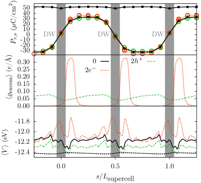
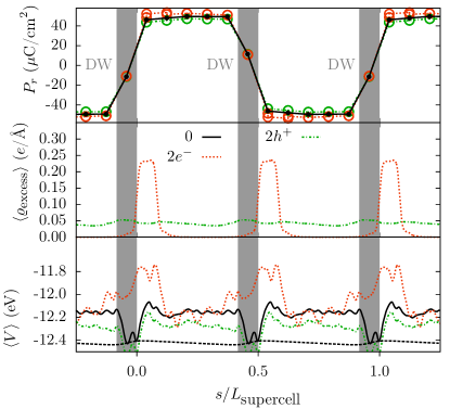
In the top panels of Figs. 3–5 we show the polarization profile, , across the DW, calculated from Eq. (1). Clearly for all DWs the polarization profile remains unchanged regardless of the system’s total charge (neutral, positively and negatively charged), meaning that the polar state of the DW structure is insensitive to charging.
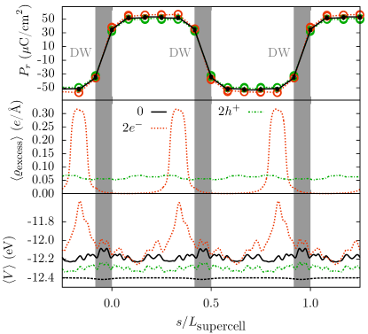
In the center panels we show the excess charge density profile upon injection of holes or electrons. In the case of electrons such additional charge localizes tightly at the DWs. In contrast the positive hole charge is distributed over the entire cell. For the 71° DW one can still observe some moderate hole localization at the DW side opposite to that where the electrons accumulate, but this is not visible for the 109° and 180° DWs. The potential resulting from such charge distribution is presented next in the bottom panels (here we show the full Kohn-Sham potential). For comparison, we also display the classical electrostatic potential estimated as in Ref. [Meyer and Vanderbilt, 2002] from the tiny reduction in the normal component of the polarization profile :
| (3) |
where is our calculated bulk electronic permittivity, is the vacuum permittivity, and and are positions left and right of the wall. However, this is too crude an approximation to capture any systematic trends in the real profiles of the full Kohn-Sham potential in the present case. Let us focus first on the Kohn-Sham potential of the neutral system (solid black line). For the 71° and 109° DWs the dominant feature in the potential is a narrow local minimum, which extends over up to two perovskite monolayers at the DW. In the case of the 180° DW the potential well becomes a shallow barrier. Similar potential wells/barriers have been found as a result of flexoelectric coupling and/or deformation potential in Ref. Morozovska et al., 2012. Despite the differences in the potential among the three DWs, excess charges distribute similarly, as described above. The charge accumulation in the case of excess electrons modifies the potential, which is now strongly repulsive at the DW (see dashed orange lines). In contrast, hole doping, where the positive charge distributes across the whole cell, affects little the general shape of the potential and its main effect is an approximately rigid energy shift (dash-dotted green lines). Thus we conclude that in a situation of excess of electrons, which can arise from intentional doping, intrinsic defects, or photo-carrier generation, the potential will present a zigzag profile along the cell. Our calculation has shown that it is possible to store about one electron per DW in our unit cell, which has a high DW density. Assuming the same excess-electron density per DW area, , and a more realistic DW separation of 140 nm Seidel et al. (2011), we arrive at a corresponding excess-electron density of , which could be entirely stored in the walls.
The effect of the DWs and of the charge accumulation on the electronic structure is analyzed next in Fig. 6, where we show the layer-resolved density of states (DOS) for the different charging situations investigated here.
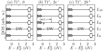
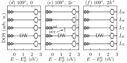
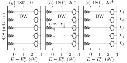
For both the neutral and the positively charged systems the DOS appears little perturbed by the presence of the DW, and it is essentially identical regardless of the layer on which it is projected. In contrast, when excess electrons are introduced, one can clearly observe the formation of two narrow peaks in the DOS localized at the layers adjacent to the DW. The gap level close to the valence band originates from occupied Fe orbitals oriented along Fe-O bonds being pushed energetically upward, while the one at higher energy is from the Fe orbitals that are directed away from Fe-O bonds and are occupied by the excess electron. The same electron trapping (small electron polaron) has been discussed in the case of charged domain walls in ErMnO3 Mundy, Julia A and Schaab, Jakob and Kumagai, Yu and Cano, Andres and Stengel, Massimiliano and Krug, Ingo P and Gottlob, DM and Doğanay, Hatice and Holtz, Megan E and Held, Rainer and others (2017) and PbTiO3 Rahmanizadeh et al. (2014). In the case of BiFeO3, we could have actually expected electron trapping instead of delocalized metallic behavior because the states of Fe at the bottom of the conduction band are relatively isolated both in space and in energy. Let us stress that the electronic polaron trap state, present here, should be distinguished from the bending (down-shift) of the entire conduction band, the latter being encountered in the case of the head-to-head, i.e. nominally charged DW Sluka et al. (2013); Bednyakov et al. (2015); Liu et al. (2015); Liu and Cohen (2017); Li et al. (2018). In the case of charged DW, the large change in (normal to the wall) should result in a large bound charge and a strong electrostatic potential variation at the wall, such that the electrostatic potential would be the dominant factor governing electron localization at the wall, and other factors like strain or tilt variations would play a minor role. In contrast, in the case of the neutral DW, electrostatic potential variations, if present, are relatively small, and other effects like strain or tilt variations can become more important. The reason why the excess electrons localize on one side of the wall appears to be related to strain and/or tilt effects. We notice in the case of the 71° and the 109° wall that before adding the excess electron, the octahedral tilt is already slightly larger on the side of the wall where the excess electron finally localizes. Once the electron polaron forms, the octahedral cage surrounding it expands, and the tilt increases further, thus lowering the energy of the trapped electron. In the case of the 180° wall, the electron also localizes on a site with large tilt, but here the left and right side of the wall are equivalent, and the electron might as well have localized on the other side. The electronic trap state might be detectable in photoemission experiments.
In both Refs. [Bhatnagar et al., 2013] and [Yang et al., 2010], the DW in BiFeO3 were found to be more conductive than the domain interior. Such DW conductivity appears to be thermally activated Bhatnagar et al. (2013), and trap states about 1 eV below the conduction band are involved in the photocurrent generation Yang et al. (2015). The deep levels which we find at electron-doped DWs could provide such trap states.
In this study we consider the idealized case of pristine DWs, which is well defined, but incomplete. Real samples contain various amounts of oxygen vacancies and/or other point defects, which may aggregate at the DWs. These may modify the electronic potential and the amount of excess electrons by acting as traps. Therefore a fully realistic picture will be obtained by considering pristine DW sections, intersected by point defects. Notably, the presence of point defects at DW could also influence the resistivity of the walls themselves. The trap states at the DW ( eV below the conduction band) are apparently deeper than those in the domain interior ( eV below the conduction band Clark and Robertson (2009)), but possibly shallower than oxygen vacancy states at the wall. Therefore oxygen vacancies at the wall may compete with the DW states as electron traps.
Summary and conclusion.
Neutral ferroelectric domain walls in BiFeO3 strongly trap excess electrons, but only weakly attract holes. The different localization behavior of electrons and holes at the walls may be understood on the basis of the electronic states which dominate the top of the valence band (delocalized O states) and the bottom of the conduction band (localized Fe states).
The potential profile at the domain walls is dominated by excess charge carriers.
Without excess electrons, the electronic potential at the domain wall exhibits mainly a well or barrier.
Once electrons are trapped in the domain walls,
they create a strong repulsive zigzag potential,
whose amplitude depends on
excess-electron and domain-wall density.
The potential at the 71° and 109° domain walls is asymmetric,
which could enable a net photovoltaic current generation,
whereas the potential at the 180° domain
wall is approximately symmetric, indicating that this wall may be photovoltaically less active.
The trap states for electrons at domain walls in BiFeO3 may be at the origin of the thermally activated domain-wall conduction found
in experiments.
Acknowledgments.
This project has received funding from the European Union’s Horizon 2020 research and innovation programme under the Marie Skłodowska-Curie Grant Agreement No. 746964–FERROVOLT and from the Czech Science Foundation (Project No. 15-04121S). Computation time was provided by the Czech Metacentrum and the Trinity Centre for High Performance Computing funded by Science Foundation Ireland. Figures were made using gnuplot, inkscape, and VESTA Momma and Izumi (2011). Pavel Márton brought this collaboration together.
References
- Seidel et al. (2011) J. Seidel, D. Fu, S.-Y. Yang, E. Alarcón-Lladó, J. Wu, R. Ramesh, and J. W. Ager III, Physical review letters 107, 126805 (2011).
- Bhatnagar et al. (2013) A. Bhatnagar, A. R. Chaudhuri, Y. H. Kim, D. Hesse, and M. Alexe, Nature Communications 4, 2835 (2013).
- Young et al. (2012) S. M. Young, F. Zheng, and A. M. Rappe, Phys. Rev. Lett. 109, 236601 (2012).
- Yang et al. (2010) S. Y. Yang, J. Seidel, S. J. Byrnes, P. Shafer, C.-H. Yang, M. D. Rossell, P. Yu, Y.-H. Chu, J. F. Scott, J. W. A. III, L. W. Martin, and R. Ramesh, Nature Nanotechnology 5, 143 (2010).
- Seidel et al. (2009) J. Seidel, L. W. Martin, Q. He, Q. Zhan, Y.-H. Chu, A. Rother, M. Hawkridge, P. Maksymovych, P. Yu, M. Gajek, et al., Nat. Mater. 8, 229 (2009).
- Lubk et al. (2009) A. Lubk, S. Gemming, and N. A. Spaldin, Phys. Rev. B 80, 104110 (2009).
- Diéguez et al. (2013) O. Diéguez, P. Aguado-Puente, J. Junquera, and J. Íñiguez, Phys. Rev. B 87, 024102 (2013).
- Wang et al. (2013) Y. Wang, C. Nelson, A. Melville, B. Winchester, S. Shang, Z.-K. Liu, D. G. Schlom, X. Pan, and L.-Q. Chen, Phys. Rev. Lett. 110, 267601 (2013).
- Ren et al. (2013) W. Ren, Y. Yang, O. Diéguez, J. Íñiguez, N. Choudhury, and L. Bellaiche, Phys. Rev. Lett. 110, 187601 (2013).
- Chen et al. (2017) Y.-W. Chen, J.-L. Kuo, and K.-H. Chew, J. Appl. Phys. 122, 075103 (2017).
- Meyer and Vanderbilt (2002) B. Meyer and D. Vanderbilt, Phys. Rev. B 65, 104111 (2002).
- Marton et al. (2010) P. Marton, I. Rychetsky, and J. Hlinka, Phys. Rev. B 81, 144125 (2010).
- Morozovska et al. (2012) A. N. Morozovska, R. K. Vasudevan, P. Maksymovych, S. V. Kalinin, and E. A. Eliseev, Phys. Rev. B 86, 085315 (2012).
- Fousek and Janovec (1969) J. Fousek and V. Janovec, J. Appl. Phys. 40, 135 (1969).
- Kresse and Furthmüller (1996) G. Kresse and J. Furthmüller, Comput. Mater. Sci. 6, 15 (1996).
- Dudarev et al. (1998) S. L. Dudarev, G. A. Botton, S. Y. Savrasov, C. J. Humphreys, and A. P. Sutton, Phys. Rev. B 57, 1505 (1998).
- Jain et al. (2013) A. Jain, S. P. Ong, G. Hautier, W. Chen, W. D. Richards, S. Dacek, S. Cholia, D. Gunter, D. Skinner, G. Ceder, and K. A. Persson, APL Materials 1, 011002 (2013).
- Mundy, Julia A and Schaab, Jakob and Kumagai, Yu and Cano, Andres and Stengel, Massimiliano and Krug, Ingo P and Gottlob, DM and Doğanay, Hatice and Holtz, Megan E and Held, Rainer and others (2017) Mundy, Julia A and Schaab, Jakob and Kumagai, Yu and Cano, Andres and Stengel, Massimiliano and Krug, Ingo P and Gottlob, DM and Doğanay, Hatice and Holtz, Megan E and Held, Rainer and others, Nat. Mater. 16, 622 (2017).
- Rahmanizadeh et al. (2014) K. Rahmanizadeh, D. Wortmann, G. Bihlmayer, and S. Blügel, Phys. Rev. B 90, 115104 (2014).
- Sluka et al. (2013) T. Sluka, A. K. Tagantsev, P. Bednyakov, and N. Setter, Nature Communications 4, 1808 (2013).
- Bednyakov et al. (2015) P. S. Bednyakov, T. Sluka, A. K. Tagantsev, D. Damjanovic, and N. Setter, Scientific Reports 5, 15819 (2015).
- Liu et al. (2015) S. Liu, F. Zheng, N. Z. Koocher, H. Takenaka, F. Wang, and A. M. Rappe, J. Phys. Chem. Lett. 6, 693 (2015).
- Liu and Cohen (2017) S. Liu and R. Cohen, J. Phys.: Condens. Matter 29, 244003 (2017).
- Li et al. (2018) M. Li, L. L. Tao, J. P. Velev, and E. Y. Tsymbal, Phys. Rev. B 97, 155121 (2018).
- Yang et al. (2015) M. Yang, A. Bhatnagar, and M. Alexe, Advanced Electronic Materials 1, 1500139 (2015).
- Clark and Robertson (2009) S. Clark and J. Robertson, Appl. Phys. Lett. 94, 022902 (2009).
- Momma and Izumi (2011) K. Momma and F. Izumi, Journal of Applied Crystallography 44, 1272 (2011).