Dynamics and Spin-Valley Locking Effects in Monolayer Transition Metal Dichalcogenides
Abstract
Transition metal dichalcogenides have been the primary
materials of interest in the field of valleytronics for their
potential in information storage, yet the limiting factor has been achieving
long valley decoherence times. We explore the dynamics of four monolayer TMDCs
(MoS, MoSe, WS, WSe) using ab initio
calculations to describe electron-electron and electron-phonon interactions. By
comparing calculations which both omit and include relativistic effects, we
isolate the impact of spin-resolved spin-orbit coupling on transport properties.
In our work, we find that spin-orbit coupling increases carrier lifetimes at the valence band
edge by an order of magnitude due to spin-valley locking, with a proportional
increase in the hole mobility at room temperature. At temperatures of 50 K, we
find intervalley scattering times on the order of 100 ps, with a maximum value
140 ps in WSe. Finally, we calculate excited-carrier generation profiles
which indicate that direct transitions dominate across optical energies, even for WSe which has an
indirect band gap. Our results highlight the intriguing interplay between spin
and valley degrees of freedom critical for valleytronic applications. Further, our work
points towards interesting quantum properties on-demand in transition metal dichalcogenides
that could be leveraged via driving spin, valley and phonon degrees of freedom.
Keywords: valleytronics, carrier dynamics, transition metal dichalcogenides, spin-valley locking
Transition metal dichalcogenides (TMDCs) represent a class of semiconducting 2D materials of significant scientific potential.Kato et al. (2004) Specifically, TMDCs are a key player in the fields of spintronics Wolf et al. (2001); Dankert and Dash (2017); Han (2016) and valleytronics Ye et al. (2016); Xiao et al. (2012) which seek to use degrees of freedom beyond charge to accelerate electronic computing and information processing. These materials offer quantum properties on-demandBasov et al. (2017); Chumak et al. (2015) with interesting possibilities to create topological states and non-equilibrium matter through driven phonon states.Hübener et al. (2018); Shin et al. (2018) Monolayer TMDCs are furnished with inequivalent valleys at the and points of the Brillouin zone Schaibley et al. (2016), due to the absence an in-plane inversion center. As a result, carriers in the and valleys acquire an additional quantum number known as their valley index or valley pseudospin. Heavy transition metal atoms in these materials introduce strong spin-orbit coupling, with large spin-splitting of opposite signs at the and valleys near the band edges, leading to spin-valley coupling Schaibley et al. (2016); Yan et al. (2017); Xu et al. (2014); De Giovannini et al. (2016). Consequently, scattering of charge carriers between valleys necessitates a simultaneous spin flip in addition to a large momentum transfer (), and is therefore expected to be a slow process Xie and Cui (2016); Song and Dery (2013).
In the current state-of-the-art in valley physics, specific valleys can be targeted and selectively populated via polarized light Mak et al. (2012); Zeng et al. (2012) and magnetic fields MacNeill et al. (2015); Aivazian et al. (2015); Srivastava et al. (2015). These methods for breaking valley degeneracy have now been well-explored, and a central limit in valleytronics remains the valley polarization lifetime which directly determines the retention time of information represented by the valley state Kim et al. (2017).
Quantifying valley polarization times in monolayer TMDCs has been led by experimental investigation Yan et al. (2017); Xie and Cui (2016); Kumar et al. (2014); Wang et al. (2013); Mai et al. (2014); Zhu et al. (2014), while theoretical work has come along only recently Molina-Sánchez et al. (2017). Difficulties in quantifying valley polarization times are clear from the wide range (from picoseconds to nanoseconds) of reported lifetimes. Outside of general experimental difficulties in 2D materials, one reason for such a discrepancy is the role of multi-particle excitations including excitons and trions. Excitons have large binding energies due to ineffective dielectric screening in 2D materials, which complicates valley population mechanisms based on optical excitation. The difference between exciton valley dynamics and free electron or hole valley dynamics is significant. While exciton valley lifetimes are expected to be short, individual electron and hole lifetimes are expected to be considerably longer, and therefore represent the best candidates for effective information storage Xu et al. (2014).
The potential for valleytronic applications is particularly enhanced by strong spin-orbit coupling at the band edges of heavy-metal monolayer TMDCs including MoS, MoSe, WS and WSe. The valence band splitting is primarily due to and orbitals of the transition metal, with splits ranging up to 0.5 eV for the heavier tungsten monolayers Zhu et al. (2011); Mak et al. (2010); Zhang et al. (2013); Zhao et al. (2013). The conduction band split is significantly smaller, as this band is mostly composed of orbitals with magnetic quantum number . This small conduction band split means that the inequivalent and valleys are susceptible to intervalley scattering Molina-Sánchez et al. (2017). The larger splitting of the valence band therefore makes this edge much more attractive for valleytronic applications. The exact role of spin-orbit coupling in carrier lifetimes and mobilities is, however, not yet known unambiguously.
In this manuscript, we investigate valley physics and transport properties of TMDCs using an ab initio framework, fully including the impact of electron-electron and electron-phonon interactions, and self-consistent spin-orbit coupling. We compare these results to spin degenerate, non-relativistic calculations, enabling us to quantify the crucial impact of spin-orbit coupling in increasing the valence band lifetimes near the and points and the corresponding hole mobilities. In particular, we show that the large spin-orbit coupling precludes intervalley scattering near the valence band edge, increasing carrier lifetimes and mobilities by an order of magnitude. We also predict energy distributions of carriers excited upon optical absorption, and find that they are dominated by direct transitions rather than indirect phonon-assisted transitions for all relevant photon energies.
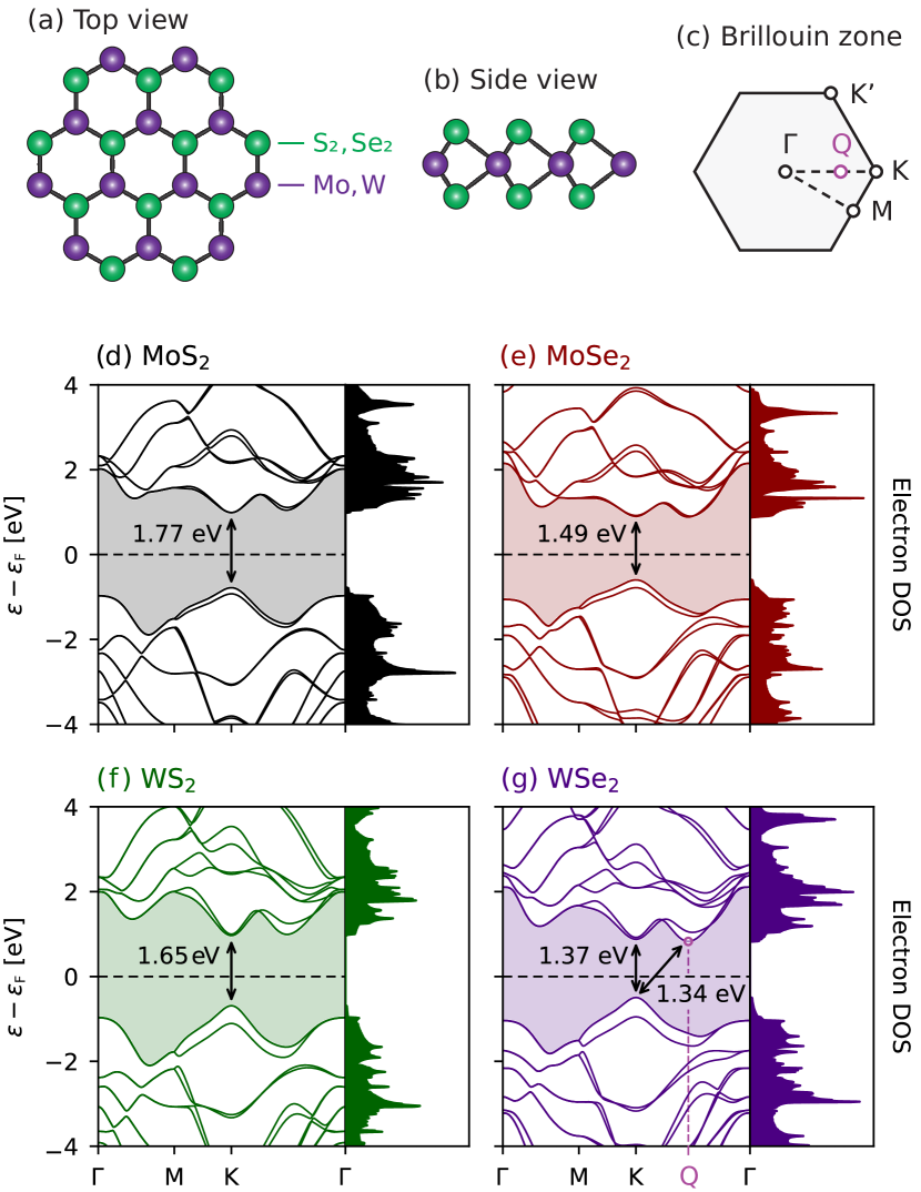
We start with first-principles electronic structure calculations of the four TMDC monolayers considered here, sulfides and selenides of tungsten and molybdenum, all of which adopt the hexagonal crystal structure illustrated in Fig. 1. Corresponding electronic band structures and densities of states are shown in Fig. 1d–g. We find that WSe is predicted to have an indirect gap, with its conduction band edge at the point rather than the point (see Fig. 1c), consistent with experimental findings Zhang et al. (2015); Hsu et al. (2017), while the remaining three materials have a direct gap at the point. All materials are mechanically stable as indicated by no imaginary frequencies in the calculated phonon band structures (see SI).

Next, we use first-principles calculations of electron-electron and electron-phonon scattering rates to predict the net carrier lifetimes, shown as a function of carrier energy in Fig. 2. The relative contributions of the two scattering mechanisms to the total scattering rate, , are shown using the color scale. Electron-phonon scattering (red) dominates the net scattering near the band edges, while electron-electron scattering picks up further from the band edges due to a quadratically increasing phase space for scattering. The scattering times near the band edges are the longest, because the phase space for electron-phonon scattering is proportional to the density of states near the carrier energy, which vanishes at the band edges.
Spin-Valley Locking Captured from First Principles. Overall, in Fig. 2, the predicted scattering times with and without spin-orbit coupling are qualitatively similar throughout, and quantitatively similar far from the band edges. However, especially near the valence band edge, spin-orbit coupling dramatically alters the electron-phonon scattering rate, increasing the net hole lifetime by about an order of magnitude in all four monolayers. At room temperature (298 K), maximum hole lifetimes in MoS and MoSe2 are 2 ps, while they exceed 4 ps in the tungsten TMDCs.

To understand the reason for lifetime enhancement due to spin-orbit coupling, Fig. 3 shows the calculated electron-phonon matrix elements (squared and summed over all phonon modes) connecting a state at the valence band edge at the point of the Brillouin zone (BZ) with the highest valence band states at all other points of the BZ. Note that without spin-orbit coupling, the results are six-fold symmetric and there is strong electron-phonon coupling between the and points, which are inequivalent due to the absence of inversion symmetry. In this case, there are two degenerate spin states at each of the and valleys, and phonons strongly couple the states with the same spin. Since these are at the same energy, these states are accessible for electron-phonon scattering and result in intervalley scattering that limits the lifetime(s) of the carriers.
Spin-orbit coupling completely changes this picture, as shown in Fig. 3. The two spin states in each of the and valleys are no longer degenerate, and the energy split occurs in the opposite direction at the two valleys. Consequently the valence band edge at the and points have opposite spins, and the intervalley scattering between these equal energy states must involve a spin flip Xu et al. (2014), which has an extremely small matrix element. This manifests in Fig. 3 as an entire half of the BZ centered on the intervalley scattering process has an essentially zero electron-phonon matrix element. The phonon states which coupled the spin-degenerate electronic states in the case without spin-orbit coupling have now been split away to an energy inaccessible at room temperature for electron-phonon scattering. This forces the carriers of a given spin to remain locked to a given valley, and this spin-valley locking produces the sharp increase in the electron-phonon lifetime of holes near the valence band edge for all four TMDCs in Fig. 2. On the other hand, the spin-orbit split at the conduction band edge is negligible and there is hence no electron lifetime enhancement compared to the non spin-orbit case.
As shown above, the rate of intervalley scattering determines the valence-band-edge carrier lifetimes. These carrier lifetimes are therefore the time for which holes remain locked to a valley, effectively the retention time of valley information in valleytronic devices. Despite a number of experimental investigations using a variety of methods, the valley retention times have not yet been conclusively determined. Using exactly the same first-principles methodology as above, we also calculate the band-edge hole lifetimes at K, where the lifetimes are expected to be longer (and more useful for valleytronics) due to lowered phase space for scattering. We find the valley retention time to be 57 ps and 67 ps for MoS and MoSe, and 62 ps and 138 ps for WS and WSe. The relative lifetime values among the four monolayers correlate with the strength of the electron-phonon coupling seen in Fig. 3. This lifetime trend also correlates with the predicted energy difference between the and valleys at the valence edge.
The methods used to calculate these lifetimes only capture processes in an atomically perfect crystal, ignoring potential interactions with defects and substrates, and therefore represent a best-case scenario for monolayer TMDC valley lifetimes. Unambiguous experimental determination of the limiting valley retention times is challenging precisely because it is impossible to disentangle substrate interactions and dopant/defect effects. Additionally, excitonic and other multi-particle effects complicate signatures from optical measurements, all of which we exclude in our theoretical predictions above. Consequently, we predict the best-case valley lifetime in monolayer TMDCs at 50 K to exceed the 100 ps scale for WSe, and to be roughly on the same order of magnitude for the others.
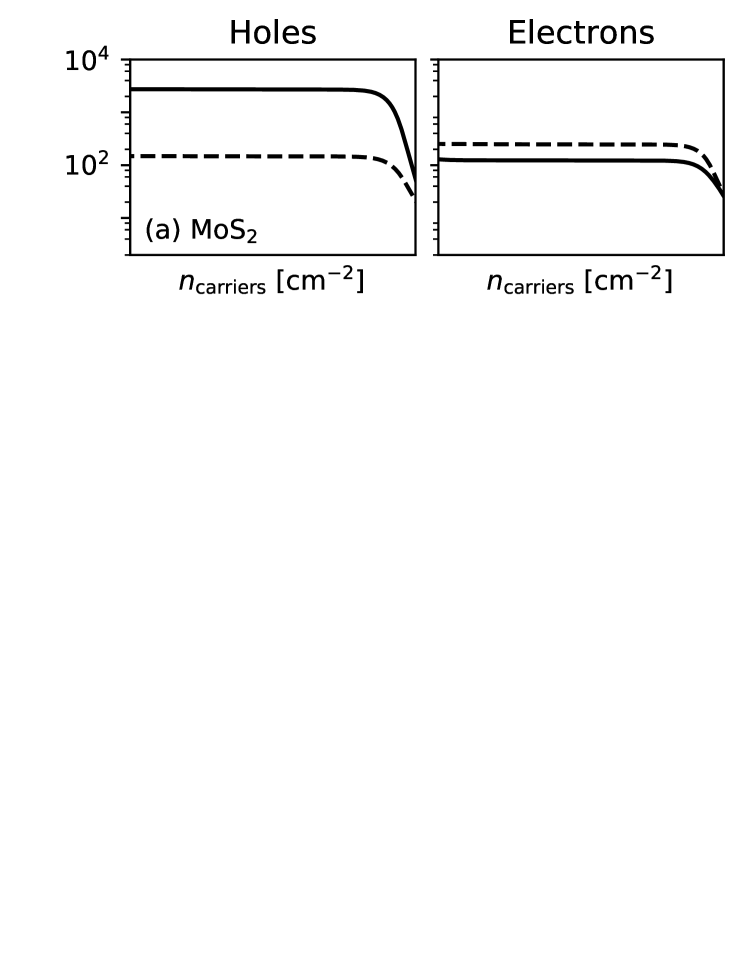
Spin-orbit Enhanced Hole Mobility. The enhancement of band-edge carrier lifetimes due to suppression of intervalley scattering should result in a corresponding increase in the carrier mobility due to spin-orbit coupling (since mobility in Drude theory). Fig. 4 shows the intrinsic carrier mobility due to electron-phonon scattering as a function of carrier density, both for electrons and holes, with and without spin-orbit coupling. As expected, the hole mobility is enhanced by over an order of magnitude when spin-orbit coupling is considered, exactly as was the case for carrier lifetimes. Previous theoretical predictions of hole mobilities in these materials,Kaasbjerg et al. (2012); Li et al. (2013); Ma and Jena (2014); Jin et al. (2014) are all below 1000 cmV-1s-1because they do not include spin-orbit interactions; our non-relativistic calculations are in good agreement with these previous studies. The trend in hole mobility is consistent with the corresponding lifetimes, with the largest hole mobility in WS cmV-1s-1.
On the other hand, electron mobility is less drastically affected by spin-orbit coupling. The differences can be explained based on the band structures calculated with and without spin-orbit coupling. In the spin-orbit case, the conduction band edge is found to be nearly degenerate between the and points (see Fig. 1). This introduces low-energy scattering between these two valleys. Meanwhile, non-relativistic calculations find the and valleys are more energetically separated, making intervalley scattering via phonons less accessible. Consequently, electron mobility is predicted to decrease due to spin-orbit coupling for some TMDCs, as shown in Fig. 4. However, in the case of WSe, the energy difference between the and conduction valleys is larger, and spin-orbit coupling increases the electron mobilities instead.
Experimentally-measured mobilities in monolayer TMDCs are smaller than theoretical predictions due to several inherent non-idealities including substrate effects, trapped impurities, air-borne adsorbates, and overall sample quality including defects and grain size Yu et al. (2017); Ahmed and Yi (2017). Our predictions shed light on the underlying physics of carrier lifetimes and transport in 2D TMDCs, underscoring the importance of spin-valley locking not just in valleytronics, but also in overall charge transport for electronic applications such as in field-effect transistors.

Finally, we investigate the energy distributions of carriers that are excited upon optical absorption in these materials, accounting for both direct and phonon-assisted transitions using our previously established first-principles methodology.Brown et al. (2016a); Narang et al. (2017); Coulter et al. (2018); Habib et al. ; Papadakis et al. (2018); Sundararaman et al. (2014); Brown et al. (2016b); Shirodkar et al. (2018) Fig. 5 show that direct transitions dominate carrier generation in all these materials, as expected for direct gap semiconductors where the band gap and optical gap are equal so that direct transitions are always allowed. However, this is also the case for the indirect-gap WSe because the small energy difference of the conduction band edges at the and points results in a small difference between the band gap and optical gap, making it behave essentially as a direct band gap semiconductor.
Conclusions. We use first-principles calculations of carrier dynamics in monolayer TMDCs with an ab initio treatment of electron-electron and electron-phonon interactions to elucidate the critical effect of spin-orbit coupling in these materials. Our results highlight the importance of spin-valley locking of holes near the valence band edge at the and , a consequence of spin-orbit coupling, on carrier lifetimes, valley retention time and charge transport. In particular, we find that spin-orbit coupling enhances the hole lifetimes and mobilities by an order of magnitude in all four materials considered here. Electron lifetimes and mobilities are less affected in comparison, due to much smaller spin-orbit coupling effects near the conduction band edge. We predict the ideal valley relaxation time in these materials at a lower temperature of 50 K to be at the 100 ps scale, with the largest value for WSe 140 ps exceeding the others by about a factor of two. While our results focus on monolayer systems, multilayer and heterostructured TMDC systems with strong spin-orbit coupling should also have similar spin-valley locking physics, which necessitate a careful analysis of the intervalley scattering mechanisms, fully accounting for the effect of phonons from a self-consistent spin-orbit coupling perspective.
Associated Content
Supporting Information. Phonon dispersion and additional details regarding calculations of optical response.
Author Information
The authors declare no competing financial interests.
Acknowledgments
This research used resources of the National Energy Research Scientific Computing Center, a DOE Office of Science User Facility supported by the Office of Science of the U.S. Department of Energy under Contract No. DE-AC02-05CH11231, as well as resources at the Research Computing Group at Harvard University. TC acknowledges support from the Danish Council for Independent Research (Grant No. DFF-6108-00667). RS acknowledges start-up funding from the Materials Science and Engineering department at Rensselaer Polytechnic Institute. PN acknowledges start-up funding from the Harvard John A. Paulson School of Engineering and Applied Sciences.
Methods
Computational Details. We used the open-source JDFTx density-functional theory software for structural relaxation, electronic band structure, phonon and electron-phonon matrix element calculations.Sundararaman et al. (2017) We carried out all calculations each with relativistic and non-relativistic ultrasoft pseudopotentials Garrity et al. (2014) to investigate the effect of spin-orbit coupling. For the exchange-correlation functional, we used the PBEsol generalized-gradient approximation Perdew et al. (2008), which yielded relaxed lattice constants within 1% of experimental values. To eliminate effect of periodic images in the out-of-plane direction, we used truncated Coulomb interactions throughout for these 2D materials.Sundararaman and Arias (2013)
All electronic calculations employed a -centered -point mesh for BZ sampling with a plane-wave energy cutoff of 30 Hartrees. Phonon properties were calculated from symmetry-irreducible perturbations in a supercell, also done both with and without self-consistent spin-orbit coupling. Directly calculating electron-phonon scattering properties in DFT is expensive due to the energy mismatch between electron and phonon scales necessitating extremely fine BZ sampling. Consequently, we convert all electron, phonon and electron-phonon properties calculated at the above ‘coarse’ BZ meshes to a basis of maximally-localized Wannier functions Souza et al. (2001) (starting from transition metal and chalcogen trial orbitals). We then interpolate these properties Giustino et al. (2007); Brown et al. (2016a) to substantially finer electron and phonon meshes with points per dimension ( total), used for all carrier scattering and optical response properties described below.
Carrier Lifetimes. The total carrier lifetime is determined by electron-electron and electron-phonon scattering, with the total scattering rate given by Matthiessen’s rule:
| (1) |
for electrons of each band at wave-vector in the two dimensional BZ. The electron-electron scattering rate is calculated from the imaginary part of the carrier self-energy, given byBrown et al. (2016a); Ladstädter et al. (2004):
| (2) |
The above expression is essentially the imaginary part of the interaction of the one-particle electronic density matrices through the dynamically screened Coulomb interaction, evaluated within the random phase approximation. This calculation is performed directly in the plane-wave basis of reciprocal lattice vectors and , and involves a sum over a full second set of electronic states (). See Ref. 40 for further details.
We calculate the electron-phonon scattering rate using Fermi’s Golden rule Brown et al. (2016a):
| (3) |
where and are energies and Fermi occupations of electrons at wave-vector in band , and are angular frequencies and Bose occupations of phonons at wave-vector with polarization index , and is the electron-phonon matrix element coupling them to final electronic state () (a three-vertex in the diagrammatic picture) with by momentum conservation. Above, the summation over accounts for phonon emission and absorption processes.
Mobility. For calculating carrier mobilities, we first evaluate carrier momentum relaxation times due to electron-phonon scattering,
| (4) |
which is identical to (3) except for an additional final factor accounting for the scattering angle between initial and final electron band velocities (defined by ). Then, we calculate the mobility by solving the linearized Boltzmann equation using a full-band relaxation-time approximation,Brown et al. (2016a); Habib et al. ; Gunst et al. (2016)
| (5) |
where the Fermi function derivative selects out carriers that contribute to transport at a particular doping level specified by Fermi level position , and where ( with and without spin-orbit coupling) is the spin-degeneracy factor. Above, the Fermi-level dependent carrier density is defined as
where is the number density of carriers in the neutral DFT calculation; this is positive for -type semiconductors with a net electron density and negative for -type semiconductors with a net hole density. By varying the Fermi level position from near the valence band edge to near the conduction band edge, we trace out the hole mobility (when ) and then the electron mobility (when ) as a function of carrier density as shown in Fig. 4.
References
- Kato et al. (2004) Y. Kato, R. C. Myers, A. C. Gossard, and D. D. Awschalom, Nature 427, 50 EP (2004).
- Wolf et al. (2001) S. A. Wolf, D. D. Awschalom, R. A. Buhrman, J. M. Daughton, S. von Molnár, M. L. Roukes, A. Y. Chtchelkanova, and D. M. Treger, Science 294, 1488 (2001).
- Dankert and Dash (2017) A. Dankert and S. P. Dash, Nat. Commun. 8, 16093 (2017).
- Han (2016) W. Han, APL Materials 4, 032401 (2016).
- Ye et al. (2016) Y. Ye, J. Xiao, H. Wang, Z. Ye, H. Zhu, M. Zhao, Y. Wang, J. Zhao, X. Yin, and X. Zhang, Nat. Nanotechnol. 11, 598 (2016).
- Xiao et al. (2012) D. Xiao, G.-B. Liu, W. Feng, X. Xu, and W. Yao, Phys. Rev. Lett. 108, 196802 (2012).
- Basov et al. (2017) D. N. Basov, R. D. Averitt, and D. Hsieh, Nature Materials 16, 1077 EP (2017).
- Chumak et al. (2015) A. V. Chumak, V. I. Vasyuchka, A. A. Serga, and B. Hillebrands, Nature Physics 11, 453 EP (2015).
- Hübener et al. (2018) H. Hübener, U. De Giovannini, and A. Rubio, Nano Letters, Nano Letters 18, 1535 (2018).
- Shin et al. (2018) D. Shin, H. Hübener, U. De Giovannini, H. Jin, A. Rubio, and N. Park, Nature Communications 9, 638 (2018).
- Schaibley et al. (2016) J. R. Schaibley, H. Yu, G. Clark, P. Rivera, J. S. Ross, K. L. Seyler, W. Yao, and X. Xu, Nat. Rev. Mater. 1, 16055 (2016).
- Yan et al. (2017) T. Yan, S. Yang, D. Li, and X. Cui, Physical Review B 95, 241406 (2017).
- Xu et al. (2014) X. Xu, W. Yao, D. Xiao, and T. F. Heinz, Nat. Phys. 10, 343 (2014).
- De Giovannini et al. (2016) U. De Giovannini, H. Hübener, and A. Rubio, Nano Letters, Nano Letters 16, 7993 (2016).
- Xie and Cui (2016) L. Xie and X. Cui, Proceedings of the National Academy of Sciences 113, 3746 (2016).
- Song and Dery (2013) Y. Song and H. Dery, Phys. Rev. Lett. 111, 026601 (2013).
- Mak et al. (2012) K. F. Mak, K. He, J. Shan, and T. F. Heinz, Nature Nanotechnology 7, 494 (2012).
- Zeng et al. (2012) H. Zeng, J. Dai, W. Yao, D. Xiao, and X. Cui, Nature Nanotechnology 7, 490 (2012).
- MacNeill et al. (2015) D. MacNeill, C. Heikes, K. F. Mak, Z. Anderson, A. Kormányos, V. Zólyomi, J. Park, and D. C. Ralph, Physical Review Letters 114, 037401 (2015).
- Aivazian et al. (2015) G. Aivazian, Z. Gong, A. M. Jones, R.-L. Chu, J. Yan, D. G. Mandrus, C. Zhang, D. Cobden, W. Yao, and X. Xu, Nature Physics 11, 148 (2015).
- Srivastava et al. (2015) A. Srivastava, M. Sidler, A. V. Allain, D. S. Lembke, A. Kis, and A. Imamoiǧlu, Nature Physics 11, 141 (2015).
- Kim et al. (2017) J. Kim, C. Jin, B. Chen, H. Cai, T. Zhao, P. Lee, S. Kahn, K. Watanabe, T. Taniguchi, S. Tongay, M. F. Crommie, and F. Wang, Science Advances 3, e1700518 (2017).
- Kumar et al. (2014) N. Kumar, J. He, D. He, Y. Wang, and H. Zhao, Nanoscale 6, 12690 (2014).
- Wang et al. (2013) Q. Wang, S. Ge, X. Li, J. Qiu, Y. Ji, J. Feng, and D. Sun, ACS Nano 7, 11087 (2013).
- Mai et al. (2014) C. Mai, A. Barrette, Y. Yu, Y. G. Semenov, K. W. Kim, L. Cao, and K. Gundogdu, Nano Letters 14, 202 (2014).
- Zhu et al. (2014) C. R. Zhu, K. Zhang, M. Glazov, B. Urbaszek, T. Amand, Z. W. Ji, B. L. Liu, and X. Marie, Physical Review B 90, 161302 (2014).
- Molina-Sánchez et al. (2017) A. Molina-Sánchez, D. Sangalli, L. Wirtz, and A. Marini, Nano Letters 17, 4549 (2017).
- Zhu et al. (2011) Z. Y. Zhu, Y. C. Cheng, and U. Schwingenschlögl, Phys. Rev. B 84, 153402 (2011).
- Mak et al. (2010) K. F. Mak, C. Lee, J. Hone, J. Shan, and T. F. Heinz, Phys. Rev. Lett. 105, 136805 (2010).
- Zhang et al. (2013) Y. Zhang, T.-R. Chang, B. Zhou, Y.-T. Cui, H. Yan, Z. Liu, F. Schmitt, J. Lee, R. Moore, Y. Chen, H. Lin, H.-T. Jeng, S.-K. Mo, Z. Hussain, A. Bansil, and Z.-X. Shen, Nat. Nanotechnol. 9, 111 (2013).
- Zhao et al. (2013) W. Zhao, Z. Ghorannevis, L. Chu, M. Toh, C. Kloc, P.-H. Tan, and G. Eda, ACS Nano 7, 791 (2013).
- Zhang et al. (2015) C. Zhang, Y. Chen, A. Johnson, M.-Y. Li, L.-J. Li, P. C. Mende, R. M. Feenstra, and C.-K. Shih, Nano Lett. 15, 6494 (2015).
- Hsu et al. (2017) W.-T. Hsu, L.-S. Lu, D. Wang, J.-K. Huang, M.-Y. Li, T.-R. Chang, Y.-C. Chou, Z.-Y. Juang, H.-T. Jeng, L.-J. Li, and W.-H. Chang, Nat. Commun. 8, 929 (2017).
- Kaasbjerg et al. (2012) K. Kaasbjerg, K. S. Thygesen, and K. W. Jacobsen, Phys. Rev. B 85, 115317 (2012).
- Li et al. (2013) X. Li, J. T. Mullen, Z. Jin, K. M. Borysenko, M. Buongiorno Nardelli, and K. W. Kim, Phys. Rev. B 87, 115418 (2013).
- Ma and Jena (2014) N. Ma and D. Jena, Physical Review X 4 (2014), 10.1103/PhysRevX.4.011043.
- Jin et al. (2014) Z. Jin, X. Li, J. T. Mullen, and K. W. Kim, Physical Review B 90, 045422 (2014).
- Yu et al. (2017) Z. Yu, Z.-Y. Ong, S. Li, J.-B. Xu, G. Zhang, Y.-W. Zhang, Y. Shi, and X. Wang, Adv. Funct. Mater. 27, 1604093 (2017).
- Ahmed and Yi (2017) S. Ahmed and J. Yi, Nano-Micro Letters 9, 50 (2017).
- Brown et al. (2016a) A. M. Brown, R. Sundararaman, P. Narang, W. A. Goddard, and H. A. Atwater, ACS Nano 10, 957 (2016a).
- Narang et al. (2017) P. Narang, L. Zhao, S. Claybrook, and R. Sundararaman, Adv. Opt. Mater. 5, 1600914 (2017).
- Coulter et al. (2018) J. Coulter, R. Sundararaman, and P. Narang, arXiv:1804.06310 [cond-mat, physics:physics] (2018), arXiv: 1804.06310.
- (43) A. Habib, R. Florio, and R. Sundararaman, J. Opt. 20, 064001.
- Papadakis et al. (2018) G. T. Papadakis, P. Narang, R. Sundararaman, N. Rivera, H. Buljan, N. Engheta, and M. Soljačić, ACS Photonics, ACS Photonics 5, 384 (2018).
- Sundararaman et al. (2014) R. Sundararaman, P. Narang, A. S. Jermyn, W. A. Goddard III, and H. A. Atwater, Nat. Commun. 5 (2014), 10.1038/ncomms6788.
- Brown et al. (2016b) A. M. Brown, R. Sundararaman, P. Narang, W. A. Goddard, and H. A. Atwater, Phys. Rev. B 94, 075120 (2016b).
- Shirodkar et al. (2018) S. N. Shirodkar, M. Mattheakis, P. Cazeaux, P. Narang, M. Soljačić, and E. Kaxiras, Phys. Rev. B 97, 195435 (2018).
- Sundararaman et al. (2017) R. Sundararaman, K. Letchworth-Weaver, K. A. Schwarz, D. Gunceler, O. Yalcin, and T. Arias, SoftwareX 6, 278 (2017).
- Garrity et al. (2014) K. F. Garrity, J. W. Bennett, K. M. Rabe, and D. Vanderbilt, Comp. Mat. Sci. 81, 446 (2014).
- Perdew et al. (2008) J. P. Perdew, A. Ruzsinszky, G. I. Csonka, O. A. Vydrov, G. E. Scuseria, L. A. Constantin, X. Zhou, and K. Burke, Phys. Rev. Lett. 100, 136406 (2008).
- Sundararaman and Arias (2013) R. Sundararaman and T. A. Arias, Phys. Rev. B 87, 165122 (2013).
- Souza et al. (2001) I. Souza, N. Marzari, and D. Vanderbilt, Phys. Rev. B 65, 035109 (2001).
- Giustino et al. (2007) F. Giustino, M. L. Cohen, and S. G. Louie, Phys. Rev. B 76, 165108 (2007).
- Ladstädter et al. (2004) F. Ladstädter, U. Hohenester, P. Puschnig, and C. Ambrosch-Draxl, Phys. Rev. B 70, 235125 (2004).
- Gunst et al. (2016) T. Gunst, T. Markussen, K. Stokbro, and M. Brandbyge, Phys. Rev. B 93, 035414 (2016).