Alloying-induced topological transition in 2D transition-metal dichalcogenide semiconductors
Abstract
Research on two-dimensional (2D) topological insulators (TIs) is obstructed due to the lack of feasible approach to grow 2D TIs in experiment. Through systematic first-principles calculations and tight-binding simulations, we proposed that alloying Os in 2D MoX2 (XS, Se, Te) monolayers is an effective approach to induce semiconductor-to-TI transition, with sizable nontrivial gap of 2537 meV. Analysis of the electronic structures reveals that the topological property mainly originates from the orbitals of Os atom. Furthermore, the TI gaps can be modulated by external biaxial strain.
Topological insulator (TI) state, discovered in recent years, is a new state of condensed matters. KaneMele1 ; KaneMele2 ; ZhangBernevig1 ; HgTeTheory ; HgTeExp ; KaneReview ; QiReview It is characterized by the combination of insulating bulk state and quantized helical conducting edge state, which exhibits intriguing quantum spin Hall (QSH) effect. The helical state provides intrinsic spin lock localized at the edge and is robust against elastic backscattering, so it is ideal for various applications that require dissipationless spin transport. KaneReview ; QiReview Although QSH state was firstly predicted in graphene which is an ideal two-dimensional (2D) material, it is difficult to observe the QSH effect in graphene due to the weak intrinsic spin-orbit coupling (SOC). Hu-1 ; Hu-2 ; Hu-3 On the contrary, significant progress on the investigation of TIs in experiment was made in quantum wells HgTeTheory ; HgTeExp ; QW-1 ; QW-2 and three-dimensional (3D) TIs BiSb-theory ; BiSb-exp ; Bi2Se3-theory ; Bi2Se3-exp1 . However, the transport properties in 3d TIs are more difficult to control than in 2D TIs, due to the gapless side surface states in 3D TIs. Therefore, 2D TIs are more promising for practical applications, since the quantized helical states only exist at the edges.
Many possible 2D TIs have been predicted in theory recently, WengHM1 ; Bansil-1 ; HeineT ; ZhaoMW but most predicted 2D TIs must be decorated by anion atoms (such as H and halogen elements) and kept away from substrate. However, it is difficult to grow freestanding 2D TIs in experiment. For example, freestanding honeycomb silicene was predicted to be TI with nontrivial gap of 1.55 meV, but the honeycomb silicene has been fabricated only on some transition metal surfaces such as Ag(111) and Ir(111). Silicene-1 ; Silicene-2 ; Silicene-3 Unfortunately, there is no evidence yet that the honeycomb silicene on these transition metal surfaces preserves the QSH state. Furthermore, large TI gaps are desired for possible applications of the 2D TIs at room temperature. Therefore, it is urgent and important to search for 2D TIs that not only have large TI gaps but also are feasible to fabricate.
Recently, 2D transition metal dichalcogenide (TMD) monolayers have attracted great attention, because they exhibit versatile electronic properties yet are chemically and physically stable. TMD-1 ; TMD-2 Most importantly, the 2D TMD monolayers can be obtained easily either through exfoliation of bulk materials or bottom-up syntheses. TMD-3 ; TMD-4 In this family, the 2D molybdenum and tungsten dichalcogenide monolayers — MoX2 and WX2 (X = S, Se or Te) — are semiconductors with sizable band gaps eV and possess fascinating valleytronic character. TMD-5 Interestingly, QSH states were predicted in 2D MoX2 and WX2 monolayers with either structural distortion LiJu or in metastable phase FangZhong . These studies provide new opportunities to explore the QSH effect in semiconducting 2D materials.
Alloying with exotic elements in semiconductors has been demonstrated as an effective method to engineer its electronic property, My-JACS ; ChengYC ; MoWSe2 ; MoWS2 which may induce intriguing physical and chemical features such as dilute magnetism ChengYC or adjustable SOC strength MoWSe2 . Therefore, it is possible to produce QSH states in 2D MoX2 and WX2 by alloying. Meanwhile, the QSH states are closely associated with the strength SOC, hence strong SOC is desired to achieve large TI gap. In this paper, we investigated the electronic properties of 2D MoX2 and WX2 monolayers alloyed with 5d transition metal elements, through first-principles calculations and tight-binding simulations. We found that Os is a good candidate to turn MoX2 and WTe2 into TIs, with nontrivial band gaps ranging from 5.3 meV to 32.3 meV. Moreover, the TI gaps can be tuned by external strain.
The structural and electronic properties were calculated with density functional theory (DFT) as implemented in the Vienna ab-initio simulation package. VASP1 ; VASP2 The interaction between valence electrons and ionic cores was described within the framework of the projector augmented wave (PAW) method. PAW1 ; PAW2 The generalized gradient approximation (GGA) was used for the exchange-correlation potentials and the SOC effect was invoked self-consistently. PBE The energy cutoff for the plane wave basis expansion was set to 500 eV. A 22 supercell was employed and the 2D Brillouin zone was sampled by a 2727 k-grid mesh. The atomic positions were fully relaxed with a criterion that requires the forces on each atom smaller than 0.01 eV/Å. The band topology is characterized by the topological invariant , with for TIs and for ordinary insulators. Z2 We adopted the so-called field scheme to calculate . n-field-0 ; n-field-1 ; n-field-2 . In addition, the band structure of the one-dimensional (1D) nanoribbon of a 2D TI exhibits edge bands within its nontrivial gap. We used the Wannier90 code Wannier-3 to obtained the hopping parameters and the tight-binding model developed by Wu WannierTools to calculate the band structures of 1D nanoribbons.
| Mo | W | ||||||
|---|---|---|---|---|---|---|---|
| S | Se | Te | S | Se | Te | ||
| 3.19 | 3.33 | 3.56 | 3.19 | 3.33 | 3.56 | ||
| 1.59 | 1.31 | 0.94 | 1.53 | 1.24 | 0.75 | ||
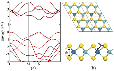
We firstly optimized the lattice constants and calculated the band structures of the Mo and W dichalcogenide monolayers. As listed in Table I, the lattice constants are slightly larger than those of their bulk counterparts TMD-1 but in agreement with previous calculations. Ding-TMD In addition, they increase as the anion changes from S to Te owing to the increasing atomic radii of the anions. However, the lattice constants do not differ visibly for MoX2 and WX2 monolayers with the same anion element. On the other hand, all MoX2 and WX2 monolayers are semiconductors with sizable band gaps () as seen in Table I. The gaps undergo an indirect-to-direct transition from the bulk to monolayer, and are enlarged due to the quantum confinement in monolayer. TMD-1 ; TMD-3 In addition, the calculated gaps are smaller than the experimental values. For instance, the calculated of MoS2 monolayer is 1.59 eV, while the experimental value is 1.8 eV. TMD-3 This is caused by the well known problem that DFT calculations usually underestimate band gaps of semiconductors. Nevertheless, the band structure plotted in Figure 1a capture the main electronic feature of the MoS2 monolayer, that is, the MoS2 monolayer is a direct-band-gap semiconductor with the valence band maximum (VBM) and conduction band minimum (CBM) locating at K point. Moreover, the SOC effect results in splitting of the valence bands around the K point as well as K point. Owing to the time reversal symmetry, the splitting leads to fascinating valley Hall effect known as valleytronics in these monolayers. TMD-5
It has been proven that doping or alloying with other transition-metal elements in MoS2 is an effective way to engineer the electronic property. MoWSe2 ; MoWS2 ; TM-dope Therefore, we choose MoS2 as a prototype to investigate the effect of alloying with 5d transition-metal elements on the electronic structures. One of the Mo atoms in a 22 supercell is replaced by a 5d transition-metal atom, resulting in an alloyed compound with concentrations of Mo and the incorporated 5d transition-metal element as 75% and 25%, respectively, as shown in Figure 1b. We considered a series of 5d transition-metal elements from Ta to Ir, and found that alloying with W does not lead to visible change of the band structures, because MoS2 and WS2 have almost the same atomic structure and close band structure. MoWSe2 ; MoWS2 Alloying with Ta, Re and Ir results in metallic property. Interestingly, MoS2 alloyed with Os (notated as Mo0.75Os0.25S2) shows a SOC induced band gap near the middle point of the path from to K, which is commonly a signature of QSH states. Accordingly, we focus on Os alloyed compounds in the following.
| Mo | W | ||||||
| S | Se | Te | S | Se | Te | ||
| 6.50 | 6.78 | 7.27 | 6.48 | 6.78 | 7.26 | ||
| 32.3 | 31.8 | 25.4 | - | - | 5.3 | ||
| 37.4 | 31.8 | 25.4 | 29.6 | 8.8 | 5.3 | ||
| 1 | 1 | 1 | - | - | 1 | ||
| 3.53 | 2.98 | 2.02 | 3.55 | 2.85 | 1.55 | ||
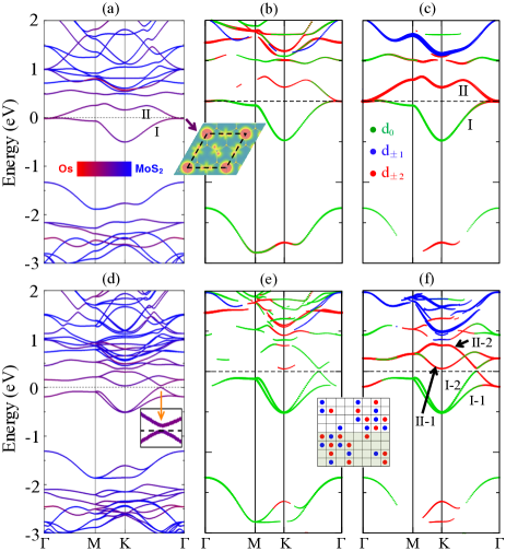
The optimized lattice constant of Mo0.75Os0.25S2 alloy is listed in Table II, which expands by 1.9% compared to that of MoS2 due to the larger atomic size of Os than Mo. To reveal the electronic property of this alloy, we plotted the atom- and orbital-resolved band structures in Figure 2. From Figure 2a, it can be seen that the Os atom hybridizes strongly with the host MoS2, which induces two bands (‘I’ and ‘II’) in the gap of MoS2. Without including the SOC effect, these bands are degenerate at the point and retain atomic orbital character as represented by the corresponding local charge density in the inset of Figure 2. Clearly, the charge density has local symmetry around the Os atoms, and characterizes apparent in-plane components of the orbitals (i.e. and ) of Mo and Os atoms. Note that the charge density around the Os atom has round shape, mainly due to the large sizes of the and orbitals which hybridize strongly with the S atoms. Accordingly, we sort the orbitals into three groups: (i) ; (ii) and ; and (iii) and . From the projections of these orbitals on the electronic bands in Figure 2b and 2c, we can see that the energy level at the of the point originates from the orbitals of both Mo and Os atoms and the weight of the Os atom is significantly larger than that of the Mo atom. As the bands propagate from the point to the M or K points, the degeneracy at the point breaks and the energy level evolves into two bands (notated as ‘I’ and ‘II’ in Figure 2c). The band ‘I’ goes downwards, with the weight of the orbitals decreasing and the weight of the orbital increasing. Finally, the band ‘I’ near the K point is contributed by the orbital completely, and the weight of the Os atom is slightly larger than that of the Mo atom. The band ‘II’ goes upwards and keeps pure state of the Os atom. For the orbitals, those of the Os atom contribute to the bands eV above the , while those of the Mo atom do not have notable contribution to the bands within the energy range in Figure 2b.
When the SOC effect is included, the degeneracy of the bands ‘I’ and ‘II’ at the point is removed with a large splitting of 0.45 eV, as shown in Figure 2d. Each of these bands further splits into two bands along the path of . Interestingly, the band ‘I-2’ goes upwards faster than the band ‘I-1’ from K to , so it crosses the . Meanwhile, the band ‘II-2’ goes downwards and crosses the at the same point. As a consequence, band inversion occurs between the bands ‘I-2’ and ‘II-2’, i.e. the and orbitals, which is a signature of nontrivial topological phase in this material. HgTeTheory As a consequence, the bands ‘I-2’ and ‘II-2’ interact with each other through the SOC Hamiltonian, yielding a nontrivial band gap of 37.4 meV. Note that the actual CBM (i.e. the minimum of the bands ‘II-1’ and ‘II-2’ as seen in Figure 2f) locates at K point rather than the crossing point, which suggests that the global gap of Mo0.75Os0.25S2 is actually an indirect band gap with a smaller amplitude of 32.3 meV. It is well known that GGA calculations usually underestimate band gaps of semiconductors, but hybrid functionals such as HSE HSE06 can predict more accurate band gaps. Indeed, our HSE calculations for Mo0.75Os0.25S2 show that the nontrivial band gap can be as large as 116 meV. Furthermore, the locates in this SOC induced gap. Accordingly, we can conclude that the Mo0.75Os0.25S2 alloy is a natural TI which does not require the gate voltage to adjust the . This is a good feature for both experimental investigations and practical applications.
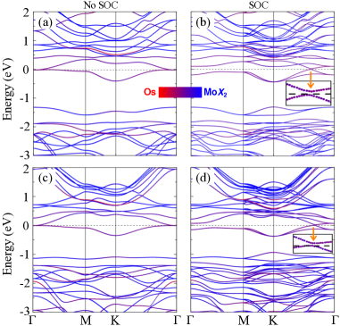
For MoSe2 and MoTe2, alloying with Os also leads to lattice expansion as listed in Table II similar to MoS2. The band structures before and after including the SOC effect are plotted in Figure 3. Clearly, the SOC has two effects on the electronic band structures. Firstly, it eliminates the degeneracy of the two bands beside the at the point. Secondly, it induces band inversion when the bands propagate from to K for both Mo0.75Os0.25Se2 and Mo0.75Os0.25Te2, which results in nontrivial band gaps of 31.8 and 25.4 meV, respectively. Note that both gaps are direct band gaps, with the VBM and CBM at the same point in the Brillouin zone. The band structures of W0.75Os0.25X2 are similar to Mo0.75Os0.25Te2. However, the ‘II-1’ band of both W0.75Os0.25S2 and W0.75Os0.25Se2 decreases significantly and crosses the , which turns the alloys into metallic. In contrast, W0.75Os0.25Te2 still possess a nontrivial band gap of 5.3 meV with . Furthermore, the direct band gap at the band-inversion point between the ‘I-2’ and ‘II-2’ bands still follow the same trend as Mo0.75Os0.25X2, as listed in Table II.
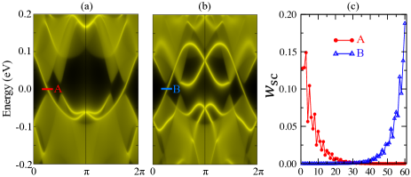
The electronic band topology can be characterized by the invariant. So we calculated of the Mo0.75Os0.25X2 alloys with the field method. n-field-0 ; n-field-1 ; n-field-2 By counting the positive and negative field numbers over half of the torus as indicated in the inset in Figure 2, we obtained for the Mo0.75Os0.25S2 alloy, clearly demonstrating the nontrivial band topology. Similarly, the invariant of the other cases is also 1, as listed in Table II. On the other hand, the topological insulators are also manifested by quantized edge states which bring about the QSH effect. KaneReview ; QiReview Therefore, we calculated the band structure of 1D nanoribbons of Mo0.75Os0.25X2 with zigzag edges. The nanoribbons consist of 60 cells and the outermost three cells are treated as edge region. Figure 4a and 4b display the edge density of states of 1D Mo0.75Os0.25Se2 nanoribbon. Apparently, there are linearly dispersive bands in the gap of 2D Mo0.75Os0.25Se2, and they are contributed by either left edge or right edge. In addition, the bands from the two edges are different, because one edge is ended by Se atoms while the other edge by Mo/Os atoms. To determine how wide the edge bands distribute, we projected the wavefunctions of the edge bands (marked as ‘A’ and ‘B’) on each cell and plotted the weights in Figure 4c. Clearly, the edge bands mainly localize within the outermost three cells and decay to zero until the thirtieth cell. Furthermore, the edge bands between and are from majority spin channel, while the edges bands between and are from minority spin channel. Therefore, there are two types of electrons with opposite spins on each edge and they are propagating along opposite directions, which are the main features of the QSH effect.
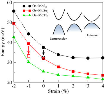
From table II, we can see that the direct band gaps of both Mo0.75Os0.25X2 and W0.75Os0.25X2 decrease as the atomic sizes of the anions increase. This is because when the Os-X bond lengths increase, the interaction between the bands ‘I-2’ and ‘II-2’ (Figure 2f) weakens. Therefore, the band gap may be engineered by external strain, as indicated by the inset in Figure 5. We calculated the band structures of Mo0.75Os0.25X2 alloys under biaxial strain from -2% to 4%, and found that the bands near the direct gaps indeed undergo similar evolutions indicated in the inset in Figure 5. As plotted in Figure 5, the nontrivial direct band gaps decrease slightly under extensile strain while increase significantly under compressive strain. For Mo0.75Os0.25S2, the compressive strain leads to metallic electronic property, because the ‘II-1’ band decreases significantly and crosses the . For Mo0.75Os0.25Se2, a compressive strain of -1% turns the gap into indirect band gap (33.2 meV), slightly larger than that without strain. When the compressive strain increases to -2%, Mo0.75Os0.25Se2 becomes metallic. The band gap of Mo0.75Os0.25Te2 keeps direct under compressive strain up to -2% and increases to 42.6 meV, 1.7 times larger than that without strain (25.4 meV). Therefore, compressive strain is an effective way to engineer the nontrivial band gap of Mo0.75Os0.25Te2.
Beside the electronic properties, the structure stability is also an important issue for the practical fabrication of the Mo0.75Os0.25X2 and W0.75Os0.25X2 alloys, which can be estimated by calculating the formation energy (). As listed in Table II, the formation energies of all the considered cases are positive, and decrease from S to Te for both MoX2 and WX2. Therefore, these alloys could not be produced in equilibrium growth condition. Nevertheless, the amplitudes of the formation energies are relatively small, especially for Mo0.75Os0.25Te2 and W0.75Os0.25Te2 (2.02 and 1.55 eV, respectively), so they may be obtained with delicate non-equilibrium growth conditions. In fact, non-equilibrium growth processes are widely used to fabricate metastable states of materials. nonequilibrium1 ; nonequilibrium2
In summary, we predicted that alloying the 2D MoX2 and WX2 monolayers with Os leads to semiconductor-to-TI transition and produces sizable nontrivial band gaps of 5.332.3 meV, based on systematic first-principles calculations and tight-binding modeling. In these alloys, the band inversion occurs between the and orbitals of the Os atom caused by the SOC effect, which plays the most important role in the QSH state. Interestingly, the TI gaps can be tuned by external biaxial strain. In particular, the TI gap of Mo0.75Os0.25Te2 can be enhanced to 42.6 meV with compressive biaxial strain of -2%. It is worth pointing that the band gaps were largely underestimated by GGA calculations, e. g. the nontrivial band gap of Mo0.75Os0.25S2 is 116 meV from HSE calculation, greatly larger than 32.3 meV (GGA). Since 2D WX2 monolayers can be fabricated in experiment effectively, our study paves the way to engineer QSH states in 2D semiconductors.
Acknowledgements This work is supported by the National Natural Science Foundation of China (11574223), the Natural Science Foundation of Jiangsu Province (BK20150303) and the Jiangsu Specially-Appointed Professor Program of Jiangsu Province.
References
- (1) C. L. Kane and E. J. Mele, Phys. Rev. Lett. 95, 146802 (2005).
- (2) C. L. Kane and E. J. Mele, Phys. Rev. Lett. 95, 226801 (2005).
- (3) B. A. Bernevig and S. C. Zhang, Phys. Rev. Lett. 96, 106802 (2006).
- (4) B. A. Bernevig, T. L. Hughes and S. C. Zhang, Science 314, 1757–1761 (2006).
- (5) M. König, S. Wiedmann, C. Brüne, A. Roth, H. Buhmann, L. W. Molenkamp, X. L. Qi and S. C. Zhang, Science 318, 766–770 (2007).
- (6) M. Z. Hasan and C. L. Kane, Rev. Mod. Phys. 82, 3045–3067 (2010).
- (7) X. L. Qi and S. C. Zhang, Rev. Mod. Phys. 83, 1057–1110 (2011).
- (8) C. Weeks, J. Hu, J. Alicea, M. Franz and R. Q. Wu, Phys. Rev. X 1 021001 (2011).
- (9) J. Hu, J. Alicea, R. Q. Wu and M. Franz, Phys. Rev. Lett. 109 266801 (2012).
- (10) J. Hu, Z. Y. Zhu and R. Q. Wu, Nano Lett. 15 2074–2078 (2015).
- (11) C. Liu, T. L. Hughes, X. L. Qi, K. Wang and S. C. Zhang, Phys. Rev. Lett. 100, 236601 (2008).
- (12) I. Knez, R. R. Du and G. Sullivan, Phys. Rev. Lett. 107, 136603 (2011).
- (13) L. Fu and C. L. Kane, Phys. Rev. B 76, 045302 (2007).
- (14) D. Hsieh, D. Qian, L. Wray, Y. Xia, Y. S. Hor, R. J. Cava and M. Z. Hasan, Nature 452, 970–974 (2008).
- (15) H. J. Zhang, C. X. Liu, X. L. Qi, X. Dai, Z. Fang and S. C. Zhang, Nat. Phys. 5, 438-442 (2009).
- (16) Y. Xia, D. Qian, D. Hsieh, L. Wray, A. Pal, H. Lin, A. Bansil, D. Grauer, Y. S. Hor, R. J. Cava and M. Z. Hasan, Nat. Phys. 5, 398-402 (2009).
- (17) H. M. Weng, X. Dai and Z. Fang, Phys. Rev. X 4, 011002 (2014).
- (18) F. C. Chuang, L. Z. Yao, Z. Q. Huang, Y. T. Liu, C. H. Hsu, T. Das, H. Lin and A. Bansil, Nano Lett. 14, 2505–2508 (2014).
- (19) Y. Ma, Y. Dai, L. Kou, T. Frauenheim and T. Heine, Nano Lett. 15, 1083–1089 (2015).
- (20) L. Y. Li, X. M. Zhang, X. Chen and M. W. Zhao, Nano Lett. 15, 1296–1301 (2015).
- (21) C. C. Liu, W. X. Feng and Y. G. Yao, Phys. Rev. Lett. 107, 076802 (2011).
- (22) P. Vogt, P. D. Padova, C. Quaresima, J. Avila, E. Frantzeskakis, M. C. Asensio, A. Resta, B. Ealet and G. L. Lay, Phys. Rev. Lett. 108, 155501 (2012).
- (23) L. Meng, Y. Wang, L. Zhang, S. Du, R. Wu, L. Li, Y. Zhang, G. Li, H. Zhou, W. A. Hofer and H. J. Gao, Nano Lett. 13, 685–690 (2013).
- (24) Q. H. Wang, K. Kalantar-Zadeh, J. N. Coleman and M. S. Strano, Nat. Nanotech. 7, 699–712 (2012).
- (25) M. Chhowalla, H. S. Shin, G. Eda, L. J. Li, K. P. Loh and H. Zhang, Nat. Chem. 5, 263–275 (2013).
- (26) K. F. Mak, C. Lee, J. Hone, J. Shan and T. F. Heinz, Phys. Rev. Lett. 105, 136805 (2010).
- (27) K. K. Liu, W. Zhang, Y. H. Lee, Y. C. Lin, M. T. Chang, C. Y. Su, C. S. Chang, H. Li, Y. Shi, H. Zhang, C. S. Lai and L. J. Li, Nano Lett. 12, 1538–1544 (2012).
- (28) X. D. Xu, W. Yao, D. Xiao and T. F. Heinz, Nat. Phys. 10, 343–350 (2014).
- (29) X. F. Qian, J. W. Liu, L. Fu and J. Li, Science 346, 1344–1347 (2014).
- (30) S. M. Nie, Z. Song, H. M. Weng and Z. Fang, Phys. Rev. B 91, 235434 (2015).
- (31) J. Hu, Y. N. Zhang, M. Law and R. Q. Wu, J. Am. Chem. Soc. 134, 13216 (2012).
- (32) Y. C. Cheng, Z. Y. Zhu, W. B. Mi, Z. B. Guo and U. Schwingenschlögl, Phys. Rev. B 87, 100401 (2013).
- (33) G. Wang, C. Robert, A. Suslu, B. Chen, S. Yang, S. Alamdari, I. C. Gerber, T. Amand, X. Marie, S. Tongay and B. Urbaszek, Nat. Commun. 6, 10110 (2015).
- (34) H. L. Li, K. Yu, Z. Tang and Z. Q. Zhu, ACS Appl. Mater. Interfaces 8, 29442–29451 (2016).
- (35) G. Kresse and J. Furthmüller, Comput. Mater. Sci. 6, 15–50 (1996).
- (36) G. Kresse and J. Furthmüller, Phys. Rev. B 54, 11169–11186 (1996).
- (37) P. E. Blöchl, Phys. Rev. B 50, 17953–17979 (1994).
- (38) G. Kresse and D. Joubert, Phys. Rev. B 59, 1758–1775 (1999).
- (39) J. P. Perdew, K. Burke and M. Ernzerho, Phys. Rev. Lett. 77, 3865–3868 (1996).
- (40) L. Fu and C. L. Kane, Phys. Rev. B 74, 195312 (2006).
- (41) T. Fukui and Y. Hatsugai, J. Phys. Soc. Jpn. 76, 053702 (2007).
- (42) D. Xiao, Y. Yao, W. Feng, J. Wen, W. Zhu, X. Q. Chen, G. M. Stocks and Z. Zhang, Phys. Rev. Lett. 105, 096404 (2010).
- (43) W. Feng, J. Wen, J. Zhou, D. Xiao and Y. Yao, Comput. Phys. Commun. 183, 1849–1859 (2012).
- (44) A. A. Mostofi, J. R. Yates, G. Pizzi, Y. S. Lee, I. Souza, D. Vanderbilt and N. Marzari. Comput. Phys. Commun. 185, 2309 (2014).
- (45) Q. S. Wu, S. N. Zhang, H. F. Song, M. Troyer and A. A. Soluyanov, Comput. Phys. Commun. 224, 405–416 (2018).
- (46) Y. Ding, Y. L. Wang, J. Ni, L. Shi, S. Q. Shi and W. H. Tang, Physica B 406, 2254–2260 (2011).
- (47) A. A. Tedstone, D. J. Lewis and P. O’Brien, Chem. Mater. 28, 1965–1974 (2016).
- (48) J. Paier, M. Marsman, K. Hummer, G. Kresse, I. C. Gerber, and J. G. Ángyán, J. Chem. Phys. 124, 154709 (2006).
- (49) M. Mahjouri-Samani, M. Tian, A. A. Puretzky, M. F. Chi, K. Wang, G. Duscher, C. M. Rouleau, G. Eres, M. Yoon, J. Lasseter, K. Xiao and D. B. Geohegan, Nano Lett. 17, 4624–4633 (2017).
- (50) J. Y. Chen, X. X. Zhao, G. Grinblat, Z. X. Chen, S. J. R. Tan, W. Fu, Z. J. Ding, I. Abdelwahab, Y. Li, D. Geng, Y. P. Liu, K. Leng, B. Liu, W. Liu, W. Tang, S. A. Maier, S. J. Pennycook and K. P. Loh, Adv. Mater. 30, 1704674 (2018).