Noise insights into electronic transport
Abstract
Typical experimental measurement is set up as a study of the system’s response to a stationary external excitation. This approach considers any random fluctuation of the signal as spurious contribution which is to be eliminated via time-averaging or, equivalently, bandwidth reduction. Beyond that lies a conceptually different paradigm – the measurement of the system’s spontaneous fluctuations. The goal of this overview article is to demonstrate how current noise measurements bring insight into hidden features of electronic transport in various mesoscopic conductors, ranging from 2D topological insulators to individual carbon nanotubes.
Back in 1918, in his research for factors limiting the performance of hot cathode amplifiers, Walter Schottky was the first to understand that discreteness of the elementary charge, , gives rise to current fluctuations in a vacuum tube 1. The noise spectral density is determined by , where is the tube’s average current. Along with the Johnson-Nyquist noise in thermal equilibrium 2, such fluctuations – now called the shot noise – represent one of the two fundamental sources of current noise in a generic conductor. Careful experiments by Hull and Williams 3 confirmed that the shot noise is observable in the current saturation regime of the vacuum tube and provides a way to measure the elementary charge as accurate as in Millikan’s oil-drop experiment. Some 70 years later, shot noise experiments demonstrated quasiparticle charge in the fractional quantum Hall effect (FQHE) 4; 5, one of the milestones in modern physics.
Diluted electron flow in a vacuum tube obeys Poissonian statistics for purely classical reasons 6. By contrast, in solid-state conductors, the shot noise arises from the random partitioning of a degenerate electron stream owing to scattering off disorder or inhomogeneities 2. This results in much richer possible outcomes of the shot noise measurement and brings valuable information about charge transport mechanism, making noise an attractive experimental tool in mesoscopic physics.
Already in the simplest case of single-mode quantum phase-coherent conductor, the partition noise acquires binomial statistics 7. Here, the limits are zero noise in the ballistic case (no scattering) and the full Schottky value in the case of negligible transmission probability, , (tunneling). In between, the spectral density of the current noise is conveniently expressed by a Fano factor , which in this case equals 8 . In multi-mode conductors the current fluctuations in different eigenchannels are independent and the overall is given by averaging over the eigenvalue distribution 2.
In metallic diffusive conductors the transmission eigenvalue distribution is universal 9, i.e. independent of the shape, length and dimensionless conductance, so is the Fano factor 10. In fact, this universality is even much stronger and persists in the classical limit, given the energy relaxation is negligible on the time scale of diffusion across the device 11. That is, perhaps, why in a number of experiments, from normal metals 12 to topological insulators 13 and semiconducting nanowires 14, is reported even though the condition of phase-coherence is apparently not fulfilled.
Obviously, current noise measurements are capable to highlight the features of electronic transport hidden in conductance experiments 2. In the ballistic regime, vanishing of the shot noise demonstrates that scattering is suppressed 8 without performing a bulky length-dependence statistics. In the localized regime, it brings information about the randomness of hopping transport 15; 16, which is otherwise encoded in the temperature dependence of the conductance 17. In the diffusive regime, various deviations from can arise from inelastic scattering 11; 18; 19 or due to the presence of built-in tunnel barriers and interfaces 20. A broader application list includes measurements of electron-phonon cooling rates 21, local 14 thermometry and spectroscopy 22, spin-to-charge conversion 23; 24; 25, investigation of Coulomb interaction effects 26; 27; 28; 29; 30 and proximity induced superconducting correlations 31; 32; 33; 34; 13.
This article gives a brief overview of our recent research and is mainly intended to illustrate the strength and, perhaps, the beauty of the noise measurements approach. The body of the paper is divided into five sections, which are largely mutually independent. In section I we investigate the noise in the hopping regime in a quantum Hall (QH) insulator. Section II is devoted to the shot noise of the edge transport in HgTe inverted band quantum wells. Section III addresses the problem of interface quality in semiconducting nanowires with metallic contacts. In section IV we study shot noise in a Coulomb blockaded carbon nanotube. Section V gives the estimate of the voltage noise in a resistive state of a superconducting film owing to spontaneous fluctuations of electronic temperature.
I I. Shot noise of a quantum Hall insulator
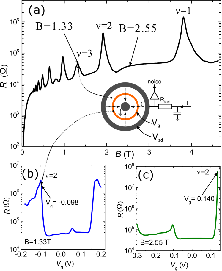
In this section, we address the statistics of current flow via insulating states realized in high-quality two-dimensional electron system (2DES) in GaAs in quantizing perpendicular magnetic fields. In the regime of integer quantum Hall effect (QHE) 35, the Fermi level of 2D electrons falls in the band of localized states and the current preferably flows perpendicular to the electric field. Dissipative transport via localized states is conveniently investigated in the geometry of Corbino disk, see the inset of fig. 1a, which allows one to get rid of the dissipationless Hall current contribution, including edge states.
Along with exponentially strong temperature () dependence of the conductance, a marked transport property of the QH insulating states is its strongly nonlinear current-voltage () response, known as the breakdown of the QHE 36. Although to our best knowledge, there exists no accepted microscopic description of the corresponding characteristics, at least qualitatively one can define two distinct transport regimes. At small enough currents, which we will address below, conduction in the band of localized states occurs via hopping scenario, nearest-neighbor or variable-range, depending on . By contrast, at very high currents, breakdown scenario is realized, during which some electrons gain enough energy to ionize a number of localized electrons, analogous to impact ionization. In this regime, the differential conductance increases by several orders of magnitude accompanied by huge current noise 37 with effective Fano factor up to , which is a clear signature of extreme avalanche bunching of electrons.
Here we concentrate on noise at small enough currents when charge transport occurs via individual hopping events within the band of localized states. In few micrometers long devices, the number of hops across the sample can well be a few tens and the noise becomes sensitive to the distribution of their probabilities, or, equivalently, resistances 17. In the regime of variable range hopping (VRH), this distribution is exponentially wide and both current and noise are dominated by the most resistive hops, so-called hard-hops 15; 16. In this case, the Fano factor is inversely proportional to the number of hard-hops, , and for can reach , as predicted by theory 38 and consistent with experiments. Remarkably, in GaAs 2DES at low and deep enough in the insulating regime the Poissonian noise with was demonstrated 39. This motivates us to study shot noise in quantizing magnetic fields, where Poissonian current statistics would enable, e.g., a direct measurement of the quasiparticle charge in the bulk of the insulating state in the FQHE.
Our device is made of high-quality 2DES of a GaAs/AlGaAs heterostructure with 2D electrons buried 200 nm below the surface. The as-grown electron density and mobility (at 4.2K) of the 2DES are, respectively, cm-2 and . On the surface of the structure, we defined a Corbino disk device, schematically shown in fig. 1a. The gate electrode encircles the inner ohmic contact and has the width and is 2.15 mm in perimeter. The distance between inner and outer ohmic contacts is . All transport measurements were performed using dc excitation in a 3He insert and the noise setup is calibrated by Johnson-Nyquist thermometry.
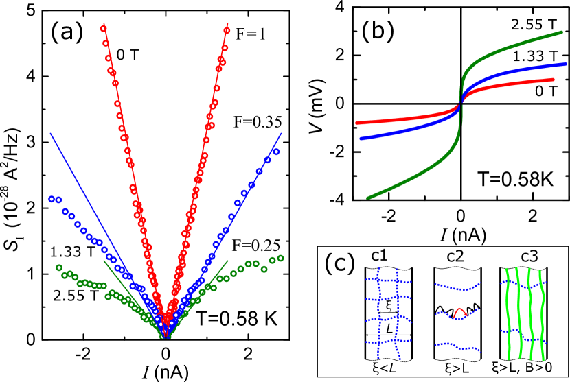
Figure 1 illustrates the procedure of the parameter choice for the noise measurements. The -field is chosen so that the Landau level filling factor in the bulk is somewhat below or above . In these cases, see the arrows in fig. 1a, the Fermi level falls in the band of delocalized states (note still hardly resolved spin gap at T) and the resistance of the device at does not exceed about 50 k. After that, we vary the gate voltage thus tuning the filling factor under the gate close to the integer value , figs. 1b and 1c. Here, the cyclotron gap opens in the 2DES under the gate and the resistance increases by at least two orders of magnitude, with exponentially strong dependence.
In figs. 2a and 2b we plot, respectively, the dependencies of shot noise and voltage across the device on the current for the chosen combinations of and . For comparison, the data obtained in the absence of magnetic field in the regime of hopping conduction at are also shown. All the curves in fig. 2b are strongly nonlinear, which is typical for conduction via localized states 40; 41; 42, and become more resistive at increasing . For instance, the linear response resistance is almost two orders of magnitude higher in T than in . However, the trend in the shot noise is opposite. As seen from fig. 2a, at increasing magnetic field the shot noise gradually drops from the Poissonian value in to in T. The finding of shot noise reduction in the insulating states in quantizing magnetic fields is the central result of this section. We briefly discuss it below.
The observation of in reproduces our previous result 39 and signals that transport in zero field occurs via VRH conduction in the regime of finite-size effect, when the width of the gate, , is not greater than the size of the critical cluster, . Compared to longer devices with in which the random resistance network is very well interconnected 17, see the sketch c1 of fig. 2c, in the finite-size regime the network splits into a number of quasi-1D hopping chains. They provide independent current paths connected in parallel 43, see the sketch c2 of fig. 2c. In a magnetic field, naively, one would expect that the finite-size effect further strengthens, for and both , the density of states at the Fermi level, and , the localization radius, are expected to decrease at increasing . In principle, there are two possibilities to explain the observed reduction of the shot noise by a factor of . The first, and fantastic, possibility would be the reduction of the quasiparticle charge in the 2DES owing to the fractional correlations 4; 5. This scenario, however, is highly unlikely since FQHE in similar structures is very weak in such small magnetic fields 44 and no signatures of the fractional gaps are seen in Fig. 1a. The second possibility is that the process of thermal activation of electrons towards delocalized states starts to contribute to transport in quantizing magnetic field. This might result from the -driven suppression of the conductance of VRH network, . Note, however, that in the QH regime thermally delocalized electrons cannot directly take part in dissipative transport since they drift long distances perpendicular to the electric field 45. Nevertheless, a variety of choices for the next hop, which emerges in the course of this drift, favors the escape of electrons from the most resistive pathways. In this way, quasi-1D hopping chains interconnect under the gate, see the sketch c3 of fig. 2c, and hopping becomes less random thereby reducing the shot noise. Our measurements demonstrate that reaching the Poissonian current statistics in quantizing magnetic fields is much more challenging compared to the case. Technically, this makes the possibility of the direct quasiparticle charge measurement in the bulk of a QH insulator extremely difficult.
II II. The noise of edge channels in a 2D topological insulator
The recently introduced topological insulators are a class of materials with an insulating bulk and conducting helical surface states 46. The core property of these states is the direct correspondence between electron spin and momentum, called spin-momentum locking, which suppresses elastic disorder scattering by the angle of . For 2D topological insulators, where the bulk material is a quantum well (QW) 47; 48; 49 or a monolayer crystal 50; 51 the surface states represent a 1D single-mode edge conduction channel, known as helical edge states. In this case, the spin-momentum locking strictly prohibits backscattering unless some spin-flip mechanism is present, the property known as topological protection. As a consequence, in the absence of time-reversal symmetry breaking, only inelastic (phase-incoherent) backscattering is allowed, which (i) dictates quantized conductance in the limit of and (ii) precludes carrier localization, which is inevitable in conventional quasi-1D conductors with a disorder. On the experimental side, the edge transport is clearly demonstrated 52; 53; 54 and, in the best devices, a poorly quantized ballistic conductance of is observed over a few micrometer length scale 48; 54; 55; 56. For longer edges, roughly linear length dependence of the resistance is reported 57; 51 with , reminiscent of phase-incoherent diffusive transport. Overall, experiment leaves a certain degree of doubt on the strength of the topological protection, especially in view of the edge transport findings in the trivial phase of InAs/GaSb QWs 58.
Non-equilibrium noise measurements in the regime of edge transport provide additional information about electron scattering and help, at least, to narrow down the list of possibilities. In Ref. 59 some of us studied 8 nm wide HgTe QWs in the disordered limit and measured . This didn’t match a well-known 2 phase-coherent 1D single-mode result , where is the transmission probability. However, in that work, the conclusion about the trivial origin of the edge transport was based on the assumption of dephasing mechanisms not related to spin, which is not the only possibility 60. The opposite limit was addressed in Ref. 22, which considered the shortest possible edges with realized in lateral p-n junctions of a 14 nm wide HgTe QWs. The observed shot noise is analyzed considering the contact leads overheating. While neither helical edge states nor diffusive multi-mode scenarios were excluded due to unknown hole-phonon coupling in p-type conduction region, the former scenario was found more consistent.
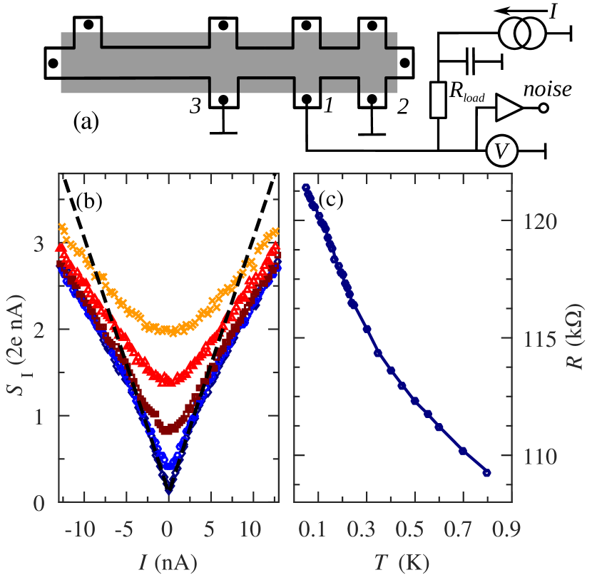
Here we report measurements of the shot noise in the 14nm HgTe QWs. Transport measurements in similar samples were performed in Ref. 54 and noise measurements in p-n junctions in Ref. 22. Samples were grown by molecular beam epitaxy, before being shaped in form of multiterminal hall-bars by wet etching and covered with a 200 nm thick insulating layer 61. On the top of the insulating layer, an Au/Ti metallic gate was deposited, covering the entire hall-bar region. In our devices the edge lengths varied between 2 and 30 , with corresponding conductances in the range . The measurements were performed in a Bluefors dilution refrigerator at electronic temperatures from mK to K, in order to exclude thermally activated bulk conduction (bulk band gap of meV reported in Ref. 54). In the present experiment, the contact 1 in fig. 3a is used to drive current through the two resistive edges 1-2 and 1-3 with lengths 5 and 10 respectively, connected in parallel. We measure both the shot noise and the DC voltage from contact 1.
Figs. 3b and 3c are the main results for this section. In the panel (b) the shot noise spectral density is plotted as a function of the device bias current at different . At the lowest mK and nA we observe a clear linear shot noise behavior with a Fano factor , see the guide line, very close to the universal diffusive value of 1/3. At increasing and/or the current noise gradually deviates down from the guide line and the effective Fano factor decreases, e.g. at K. At the same time, see fig. 3c, the linear response resistance, , exhibits a weakly insulating temperature dependence increasing roughly by 10 % at decreasing from 0.8 K to 80 mK. In the following, we briefly discuss these results in the context of possible transport scenarios.
On the one hand, the observation of shot noise Fano factor very close to the universal value in diffusive conductors 11; 10 evidences diffusive edge transport in our devices, with negligible energy relaxation. On the other hand, that diffusive transport is observed for edge conductances much smaller than , obviously, implies strong dephasing, regardless of the edge transport scenario 9; 62. In the case of trivial multi-mode edge conduction, slightly insulating -dependence of the resistance in fig. 3c can be attributed to a weak localization correction in the limit of dephasing length smaller than localization length. In this case, the correction to the universal value is still expected to be small, yet positive 2. In the case of helical edge states, our data allow to exclude e-e scattering as a relevant backscattering mechanism in generic helical liquids 63; 64. In this situation, one would expect metallic dependence of the resistance and Fano factor 18; 19 , which is opposite to our experiment. The microscopic model of random charge-puddles coupled to helical edge states 65 is inconsistent with the data in fig. 3c. However, a more general phenomenological model of Ref. 60 captures our noise data correctly, provided negligible energy relaxation and sufficient spin-flip rate within a puddle. In order to explain the behavior of , however, an increase of the spin-flip rate at decreasing is necessary, which might be a problem for theory in our temperature range. Scenarios of time-reversal symmetry breaking owing to magnetic impurities 66 or hyperfine interaction 67; 68 predict negative corrections to the conductance without energy relaxation to the bath, which would be qualitatively consistent with our data. Yet, the numerical estimates of these effects in HgTe QWs are unrealistically small 66; 68.
III III. Noise probes interface transparency in hybrid structures
The theoretical possibility to realize hybrid topological materials 69 has recently led to the revival of experimental interest in inducing superconducting correlations into semiconducting materials. Currently, the most relevant direction is proximitizing quasi-one-dimensional nanowires (NWs) either grown individually 70; 33; 71 or realized in 2D electron gas 72; 73; 74. For all possible applications, the quality of both the one-dimensional conductor and of the semiconductor-superconductor interfaces are of paramount importance. In this section, we demonstrate how noise measurements may complement simple transport measurements in order to better track the possible influence of any present potential barriers.
To illustrate this idea we present experimental data obtained on individually grown semiconductor NWs with Al interfaces. Unintentionally doped catalyst-free InAs NWs were grown by MBE on a Si(111) substrate 75. The NWs were then detached from the substrate in an ultrasonic bath and drop-casted on a piece of commercial -doped Si wafer covered by of SiO2. In order to remove the native oxide layer from the contact regions, prior to the electron beam evaporation of Al otherwise identical samples NW1 and NW2 were in-situ exposed to Ar ion gun ( sccm Ar flow, discharge and accelerating voltage) during and minutes, respectively. The latter time is presumably too large and might have led to over-etching of the device NW2 under electrodes and, thus, to bad Al/InAs interfaces. The evaporation was performed in a Plassys MEB 550S system. The measurements were performed in a dry Bluefors dilution refrigerator with the electronic temperature of , verified by noise thermometry.
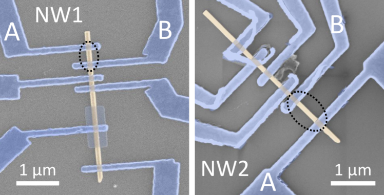
False color SEM images of the studied devices are shown in fig. 4. The Al contact electrodes are nominally -wide. We will discuss the data obtained on the NW sections between electrodes A and B, which are and long for devices NW1 and NW2, respectively.
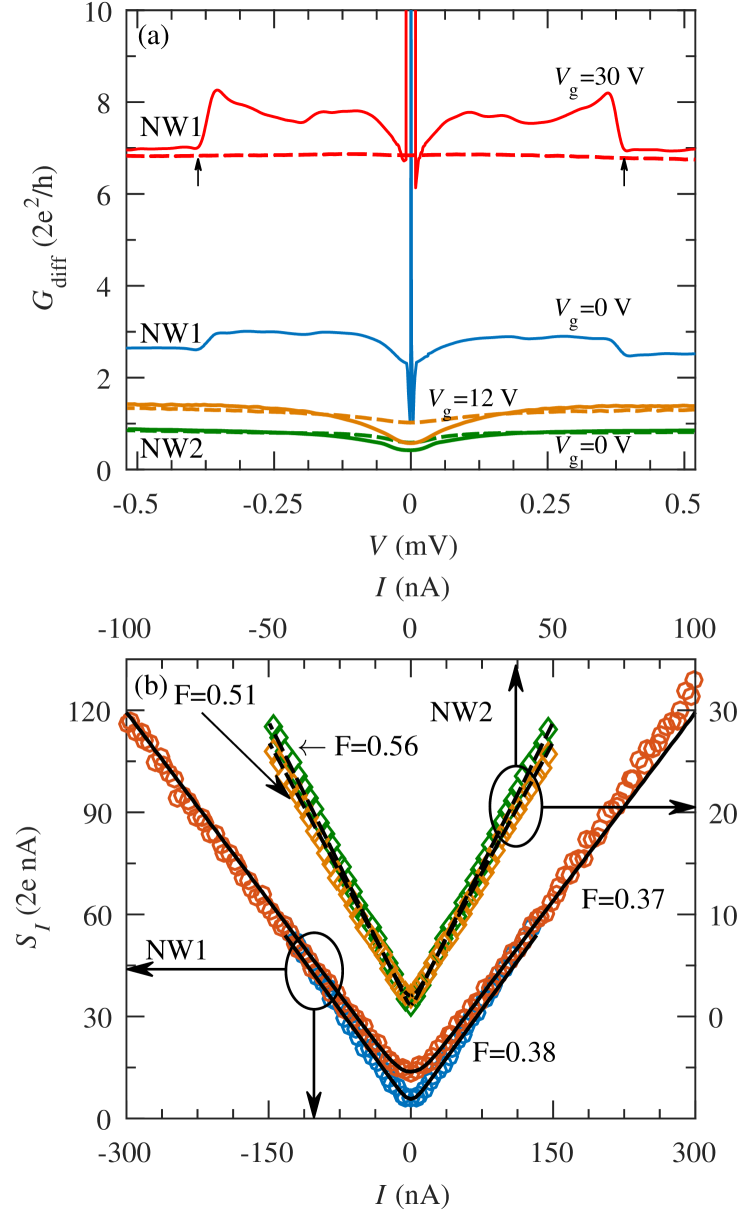
In fig. 5(a) we plot the bias dependence of the differential conductance, , both in zero, (solid lines), and non-zero, (dashed lines), magnetic fields for various back gate voltages . In the shorter device NW1 we observe the supercurrent at and the large zero-bias conductance peak at . In fig. 5(a) these features are obtained by numerical differentiation of the -curves, while the larger-bias data are obtained by the lock-in measurements with ac current modulation of rms.
The comparison of traces obtained in superconducting and normal states may indicate the better quality of Al/InAs interfaces in the NW1 device compared to the NW2 device. Indeed, in NW1 in we observe the increase of at sub-gap voltages, starting abruptly at approximately twice the superconducting energy gap of Al: , see vertical arrows. Microscopically, this sub-gap enhancement above the normal-state conductance reflects the Andreev reflection charge transport taking place at Al/InAs interfaces and is distinctive for transmissive SNS structures 76; 77. The observation of the supercurrent/large zero-bias conductance further suggests the good quality of the interfaces in the device NW1. We note that these features remain in NW1 at lower gate voltages when the normal-state resistance of the device is on the order of . On the contrary, in NW2, in the sub-gap region at bias voltages , we observe the decrease of the conductance below the normal-state value in all the available range of . Such a behavior is inherent in nanostructures of a tunnel type 71 and reflects the fact that Andreev reflection requires two transmission events 78. The normal-state conductance is thus higher being proportional to the first power of transmission eigenvalues.
Altogether, the data of fig. 5(a) display the difference between the devices NW1 and NW2. This difference is additionally manifested in its shot noise in the normal state in magnetic field. In fig. 5(b) we demonstrate the shot noise of the devices NW1 (left-bottom axes) and NW2 (right-top axes, the scales on both axes are enlarged by a factor of and the data are vertically offset by for clarity) obtained in at the same values of as in fig. 5(a). For both samples we observe linear -dependencies characteristic of elastic transport. In NW1, the Fano-factor is almost independent of and is only slightly greater than the universal value , characteristic for diffusive elastic conduction mechanism. The shot noise in NW2 is significantly greater with , slightly increasing with increasing resistance in the available gate voltage range. In the following we discuss the device NW2 since for NW1 we cannot reliably exclude the influence of experimental uncertainty. In principle, the conductance diminishing in the sub-gap region and the accompanying enhanced shot noise in the device NW2 might result from the possibly present tunnel barriers 62. These might be caused by the short-period wurtzite segments in our polytypic InAs NWs 79 or, alternatively, represent the barriers in the vicinity of Al/InAs interfaces, which result from disorder or band bending due to change in electrostatics after deposition of Al 80.
The Fano-factor of the phase-incoherent diffusive conductor with planar tunnel barriers is given by
where is the resistance of the th barrier, is the number of barriers and is the sum of the resistances of diffusive pieces. According to this expression, the experimental observation of in NW2 then necessarily requires that the resistance of the device is dominated by the resistance of a single tunnel barrier with . Were it the interfacial barrier, we can roughly estimate the ratio of the normal-state and zero-field zero-bias conductances using the result of Nazarov 81. Numerically, we find and at and , respectively, which is in reasonable agreement with the experimentally observed ratios of and . While this may point in favor of the interfacial barrier, we emphasize that our data also don’t exclude the structural defect scenario. Concluding this section, we note that the data presented here is, to our best knowledge, the first attempt to verify the role of the built-in tunnel barriers from simultaneous transport and noise measurements in diffusive semiconductor-superconductor hybrid structures.
IV IV. Shot noise in carbon nanotube quantum dots
The randomness of electronic transport in mesoscopic conductors in many cases can be understood within the framework of non-interacting electrons 2. At first glance, this may seem surprising since in the absence of interactions electrons must be uncorrelated and obey Poissonian statistics, just like in Schottky’s vacuum tube. In reality, degenerate electrons in solids are extremely correlated owing to the Pauli exclusion principle 7, which is the ultimate reason for the shot noise vanishing in a ballistic conductor 8. For the same reason, intrinsic ordering of the incident flux can be directly observed in cross-correlation experiments with electronic beams in the QH edge channels 82. On top of this, additional correlations can arise thanks to the proximity with a superconductor 2 or due to Coulomb interactions between electrons. In the latter case, which we focus on in this section, such effects are most pronounced in quantum dots (QDs), where Coulomb energy represents the largest energy scale.
The simplest (two-terminal) quantum dot is a conductive island weakly coupled to macroscopic leads via tunnel barriers. Here, we investigate a single-walled carbon nanotube (SWCNT) QD with thermally evaporated Ti/Pd/Au leads with thicknesses of, correspondingly, 0.3/5/60 nm and fabricated via standard e-beam lithography technique. The SWCNTs were grown by aerosol CVD process 83; 84 and dry deposited on a Si/SiO2 substrate. Unlike in lateral quantum dots formed, e.g., in GaAs, here, tunnel barriers naturally result from the Schottky barrier between the SWCNT and the contact metal. The chemical potential of the dot is tuned by the back gate voltage . The atomic force micrograph of the device is shown in fig. 6 (inset). Nanotube’s height measured before all fabrication steps was approximately 1.3 nm, which to best of our knowledge is an indication of a bundle of SWCNTs, since the minimum diameter of a single nanotube we observed was in the range of 0.6 - 0.8 nm. On top of the SWCNT (faint line) three metallic contacts are evaporated, dividing it into two sections, each approximately 400 nm long. Throughout the experiment, the center contact 3 was grounded, the rightmost contact 4 was floating and the dc bias voltage with a small ac modulation was applied to the left contact 1 via the input of a home-made I-V converter ( V/A). The current was measured using standard lock-in technique at 31 Hz modulation frequency. The resonant tank-circuit with the central frequency of and a load resistor was connected to the contact 1 for the shot noise measurements. As usual, the signal was calibrated using Johnson-Nyquist noise thermometry. We used side gates 2 and 5 to check that Coulomb coupling between the two dots on either side of the central contact 3 is negligible, hence possible charging events on the right QD are irrelevant for the transport and noise measured in the left QD. All the data discussed below are obtained at a bath temperature of 0.5 K in a liquid 3He insert with grounded gates 2 and 5.
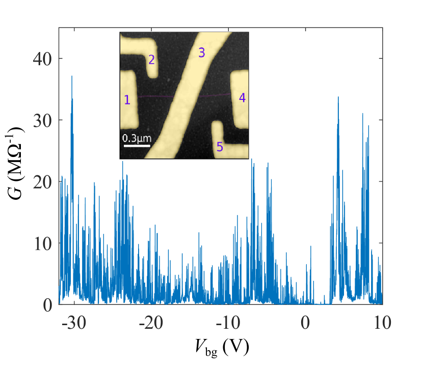
In fig. 6 (body) we plot -dependence of the linear response conductance of the left SWCNT QD. Within a wide range of we observe pronounced Coulomb blockade oscillations of irregular amplitude and spacing between neighboring peaks. At slightly positive in the range the oscillations are suppressed, indicating the energy gap in the spectrum characteristic for semiconducting SWCNTs. Depending on ranges, both oscillations with and without well-developed Coulomb blockade are seen. For some well-developed oscillations (ratio between conductance maxima and minima at least 10) we performed standard finite bias spectroscopy and found the addition energy, which varies between 1 meV and 5 meV. This scatter is not expected for an individual SWCNT QD, where the fluctuations of single-particle level spacing are typically much smaller than Coulomb energy, determined by the QD capacitance 85; 86. While it is difficult to draw a definitive conclusion, this might be another indication of a bundle of few SWCNTs connected in parallel. We also cannot exclude an impact of multi-subband transport at large negative . In this case, transport irregularities can be related to a complex interplay of single-particle energy spectrum with intra-SWCNT and inter-SWCNT Coulomb interactions. Below we concentrate on current noise measurements within an arbitrarily chosen pair of adjacent Coulomb blockade resonances and correlate different transport regimes with the current noise measurements.
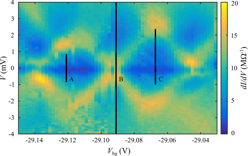
Fig. 7 shows a standard color-scale plot of differential conductance as a function of bias voltage and . Note that owing to appreciable temporal drifts in our device this data cannot be directly compared to the data of fig. 6, which were recorded more than a week before. The data of fig. 7 demonstrates suppressed conductance inside diamond-shaped Coulomb blockade regions. Here, sequential tunneling is forbidden and finite current through the QD occurs only via higher-order co-tunneling processes, which conserve the charge on the QD 87. Figs. 8a, 8b and 8c, axes on the rhs, show three traces of the differential conductance, , as a function of obtained for fixed cuts of the Coulomb diamonds (marked by solid lines in fig. 7). Traces A and C demonstrate wide conductance minima inside the Coulomb blockade region, followed by conductance maxima at bias voltages roughly corresponding to the boundaries of the Coulomb diamond structure. As usual, this behavior signals the transition from high order co-tunneling processes at low biases to sequential tunneling at high biases. By contrast, trace B exhibits conductance maximum around , indicating that charge transport near the Coulomb resonance occurs mainly owing to the sequential tunneling via a single quantum level of the SWCNT QD.
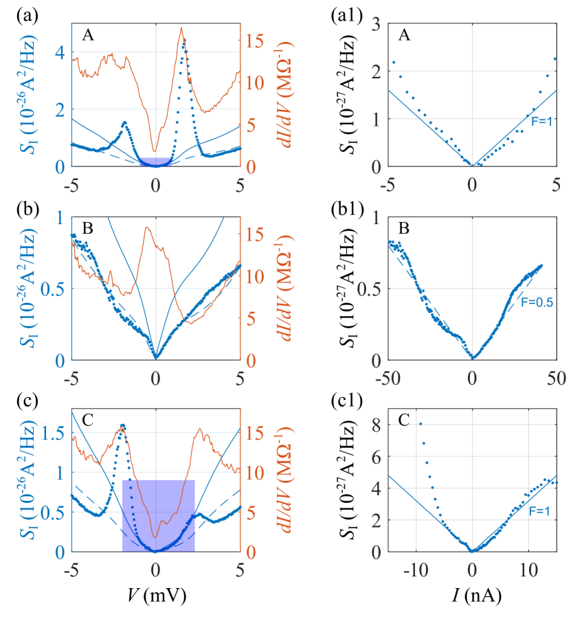
The current noise brings more information about microscopic processes underlying SWCNT QD transport. Figs. 8a, 8b and 8c, axes on the left, show the spectral density of current fluctuations measured for the same set of . Depending on the gate voltage position, three distinct types of behavior are observed. First, at small currents and well inside the Coulomb diamonds, see the panels corresponding to traces A and C, the measured noise is close to Poissonian value , as shown by solid guide lines. This behavior is expected for the shot noise of elastic co-tunneling process, during which the QD state remains in its ground state 87; 88; 89; 28. Qualitatively, in this case, the electron sees the QD as a single extremely opaque tunnel barrier, just like in a usual non-interacting case 87. For convenience, we also replotted the low bias regions highlighted in figs. 8a and 8c, in the form of vs , respectively, in panels (a1) and (c1) of fig. 8. In this representation the conventional linear shot noise behavior with is evident.
Second, when the QD chemical potential is tuned to the position of Coulomb resonance, see the panels (b) and (b1) of fig. 8 corresponding to the trace B, the noise is reduced compared to the Poissonian value. The reduction is roughly by a factor of 2 and slightly depends on current, see the dashed guide line with . The observation of is a signature of sequential tunneling in which transport through the QD occurs via two independent tunneling processes across the QD-lead barriers 87; 88; 90; 91; 89; 28. Similar to the non-interacting double-barrier case, this effect is a consequence of current conservation 2; 87 and indicates that QD-lead barriers are nearly identical. Close to linear dependence in this case is evident from panel (b1). Passing, we note that at some at small currents we have obtained , which is difficult to understand in a conventional framework of shot noise in the regime of sequential tunneling. In these situations, however, the SWCNT resistance was typically below 100 k and clear Coulomb diamond structure was not observable.
Third, and perhaps the most striking, is the observation of super-Poissonian noise peaks, sometimes with , around certain values of and , see the data for traces A and C near mV. Although much more pronounced, this effect resembles super-Poissonian noise maxima observed in random hopping transport via interacting localized states in the insulating phase of n-GaAs transistor 16. In carbon-nanotube QDs the shot noise several times the Poissonian value was measured in the regime of inelastic co-tunneling 90; 28. In general, such a behavior is explained by modulation of the QD current, which occurs owing to the very fast random switching between different quantum states in the regime of Coulomb blockade 87; 88; 92. Giant noise then is a pure interaction effect not observed, e.g., in SWCNTs in a Fabry-Perot transport regime 91. In Markovian approximation 93; 87 the modulation noise acquires Lorentzian spectrum and covers the frequency range up to the inverse correlation time of the switching process. Measurements in SWCNTs in the gigahertz regime indicate that the correlation time falls in the range of a few 10 ps 90; 89, which effectively gives rise to super-Poissonian white noise at sub-10 GHz frequencies 28, including those used in the present experiment.
As seen from figs. 8a and 8c, super-Poissonian noise maxima correlate with the maxima of differential conductance, which is a clear signature of the modulation noise. Apart from that, however, the low quality of the Coulomb diamonds in our experiment, see fig. 7, precludes us from unequivocal identification of the microscopic SWCNT QD states participating in the switching process.
V V. Noise and fluctuations of temperature at a resistive transition
Spontaneous fluctuations of current in a conductor at the onset of the transition to the superconducting state (called below the resistive transition) are believed to provide microscopic insight into superconducting correlations. More than 50 years ago, giant low-frequency noise in type-II superconducting films in the magnetic field was associated with the correlated motion of bunches of magnetic vortices 94. Much smaller noise in disordered type-I films in zero field was interpreted in terms of the motion of independent vortices, emerging from unbinding of vortex-antivortex pairs in a 2D superconductor 95. Giant noise can also be observed in superconducting weak links 96, originating from fluctuations of the order-parameter 97, multiple 98 or individual quantum 99 phase slips. In the context of transition edge thermometry 100, it was argued that giant noise at the resistive transition can also originate from spontaneous fluctuations of the electronic temperature. Here we present the ab-initio estimate of such noise, which is insensitive to the microscopic features of the resistive transition and can dominate the noise spectrum in a wide frequency range.
In thermodynamic equilibrium mean squared fluctuation of the electronic temperature, , is expressed as 101:
| (1) |
where is the (electronic) heat capacity and is the Boltzmann constant. We are interested in the spectral density of fluctuations as a function of frequency, , which obeys the standard identity . Note, that is twice the Fourier transform of the correlation function 93 and can be obtained, e.g., in ac-heating experiments 102. Typically, such experiments identify Lorentzian-shaped frequency response 103, with characteristic correlation time of a temperature fluctuation, , given by the ratio of and the heat conduction rate to the external bath, , (both per unit volume), . Below we assume that heat conduction is determined by the electron-phonon (e-ph) cooling rate, , and derive from eq. (1) , omitting an insignificant for our purposes numerical factor of order unity.
Fluctuations of give rise to fluctuations of the resistance, , and hence to voltage fluctuations in the current biased device. These fluctuations are strongest at the resistive transition, where has the strongest temperature dependence. The spectral density of such voltage fluctuations is given by 102 , where is the average current and is the spectral density of the resistance fluctuations. Since , we obtain:
| (2) |
where, is the total e-ph heat conduction of the sample.
In order to estimate the magnitude of voltage fluctuations, we assume that the current biased superconducting film in the vicinity of the sharp resistive transition remains in local thermal equilibrium. In other words, we assume that while Joule heating slightly raises the electronic temperature above the bath, , all the electronic degrees of freedom are mutually equilibrated and the characteristics of the device simply follows the temperature dependence of the resistance . This assumption is reasonable at least in some cases, see Ref. 104. Since is related to the e-ph cooling rate , we obtain:
| (3) |
Under our assumptions, the spectral density of voltage fluctuations is simply determined by the temperature dependence of the resistive transition with as a parameter. Obviously, noise predicted by eq. (3) can very well exceed the equilibrium Johnson-Nyquist value , provided the width of the resistive transition, , is small enough. It’s also straightforward to see that for high-quality films with in the range of a few , our estimate of is much higher than the noises caused by quantum phase slips 99 or by fluctuations of the order-parameter 97. Unlike these mechanisms, however, the noise owing to thermal fluctuations is insensitive to the microscopic nature of the resistive transition and its spectral density is cutoff at a frequency on the order of the inverse e-ph relaxation time 103.
VI Summary
In summary, we discussed several examples how non-equilibrium noise measurements shed light on microscopic aspects of mesoscopic electron transport. Such experiments directly probe electronic correlations, elastic scattering, and energy relaxation in various transport regimes, from normal to superconducting and from ballistic to localized. Hopefully, in this short review, we demonstrated that measuring noise is not only a powerful but also a beautiful approach in experimental condensed matter physics.
We are grateful to Z.D. Kvon, J. Becker and D. Ruhstorfer for help and acknowledge discussions with K.E. Nagaev, T.M. Klapwijk, A.V. Semenov, A.G. Semenov, M.A. Skvotsov, G.E. Fedorov and A.A. Zhukov. The experimental work was partly supported by the RSF Project No. 16-42-01050 and theoretical estimation in section V was supported by the RSF Project No. 17-72-30036. G.K. acknowledges support from DFG-Project No. KO-4005/5-1.
References
- Schottky (1918) W. Schottky, Annalen der Physik 362, 541 (1918).
- Blanter and Büttiker (2000) Y. Blanter and M. Büttiker, Physics Reports 336, 1 (2000).
- Hull and Williams (1925) A. W. Hull and N. H. Williams, Phys. Rev. 25, 147 (1925).
- de Picciotto et al. (1997) R. de Picciotto, M. Reznikov, M. Heiblum, V. Umansky, G. Bunin, and D. Mahalu, Nature 389, 162 (1997).
- Saminadayar et al. (1997) L. Saminadayar, D. C. Glattli, Y. Jin, and B. Etienne, Phys. Rev. Lett. 79, 2526 (1997).
- Schönenberger et al. (2001) C. Schönenberger, S. Oberholzer, E. Sukhorukov, and H. Grabert, arXiv preprint , 0112504 (2001).
- Levitov and Lesovik (1993) L. Levitov and G. Lesovik, Pis ma Zh. Eksp. Teor. Fiz. 58, 225 (1993).
- Reznikov et al. (1995) M. Reznikov, M. Heiblum, H. Shtrikman, and D. Mahalu, Phys. Rev. Lett. 75, 3340 (1995).
- Beenakker (1997) C. W. J. Beenakker, Rev. Mod. Phys. 69, 731 (1997).
- Beenakker and Büttiker (1992) C. W. J. Beenakker and M. Büttiker, Phys. Rev. B 46, 1889 (1992).
- Nagaev (1992) K. E. Nagaev, Physics Letters A 169, 103 (1992).
- Henny et al. (1999) M. Henny, S. Oberholzer, C. Strunk, and C. Schönenberger, Phys. Rev. B 59, 2871 (1999).
- Tikhonov et al. (2016a) E. S. Tikhonov, D. V. Shovkun, M. Snelder, M. P. Stehno, Y. Huang, M. S. Golden, A. A. Golubov, A. Brinkman, and V. S. Khrapai, Phys. Rev. Lett. 117, 147001 (2016a).
- Tikhonov et al. (2016b) E. S. Tikhonov, D. V. Shovkun, D. Ercolani, F. Rossella, M. Rocci, L. Sorba, S. Roddaro, and V. S. Khrapai, Scientific Reports 6 (2016b), 10.1038/srep30621.
- Kuznetsov et al. (2000) V. V. Kuznetsov, E. E. Mendez, X. Zuo, G. L. Snider, and E. T. Croke, Phys. Rev. Lett. 85, 397 (2000).
- Safonov et al. (2003) S. S. Safonov, A. K. Savchenko, D. A. Bagrets, O. N. Jouravlev, Y. V. Nazarov, E. H. Linfield, and D. A. Ritchie, Phys. Rev. Lett. 91, 136801 (2003).
- Shklovskii and Efros (2013) B. Shklovskii and A. Efros, Electronic Properties of Doped Semiconductors, Springer Series in Solid-State Sciences (Springer Berlin Heidelberg, 2013).
- Nagaev (1995) K. E. Nagaev, Phys. Rev. B 52, 4740 (1995).
- Kozub and Rudin (1995) V. I. Kozub and A. M. Rudin, Phys. Rev. B 52, 7853 (1995).
- Nazarov (1994a) Y. V. Nazarov, Phys. Rev. Lett. 73, 134 (1994a).
- Roukes et al. (1985) M. L. Roukes, M. R. Freeman, R. S. Germain, R. C. Richardson, and M. B. Ketchen, Phys. Rev. Lett. 55, 422 (1985).
- Piatrusha and Khrapai (2017) S. Piatrusha and V. Khrapai, in 2017 International Conference on Noise and Fluctuations (ICNF) (IEEE, 2017).
- Meair et al. (2011) J. Meair, P. Stano, and P. Jacquod, Phys. Rev. B 84, 073302 (2011).
- Arakawa et al. (2015) T. Arakawa, J. Shiogai, M. Ciorga, M. Utz, D. Schuh, M. Kohda, J. Nitta, D. Bougeard, D. Weiss, T. Ono, and K. Kobayashi, Phys. Rev. Lett. 114, 016601 (2015).
- Khrapai and Nagaev (2017) V. S. Khrapai and K. E. Nagaev, JETP Letters 105, 18 (2017).
- Roche et al. (2004) P. Roche, J. Ségala, D. C. Glattli, J. T. Nicholls, M. Pepper, A. C. Graham, K. J. Thomas, M. Y. Simmons, and D. A. Ritchie, Phys. Rev. Lett. 93, 116602 (2004).
- Yamauchi et al. (2011) Y. Yamauchi, K. Sekiguchi, K. Chida, T. Arakawa, S. Nakamura, K. Kobayashi, T. Ono, T. Fujii, and R. Sakano, Phys. Rev. Lett. 106, 176601 (2011).
- Harabula et al. (2018) M.-C. Harabula, V. Ranjan, R. Haller, G. Fülöp, and C. Schönenberger, Phys. Rev. B 97, 115403 (2018).
- Inoue et al. (2014) H. Inoue, A. Grivnin, N. Ofek, I. Neder, M. Heiblum, V. Umansky, and D. Mahalu, Phys. Rev. Lett. 112, 166801 (2014).
- Tikhonov et al. (2014) E. S. Tikhonov, M. Y. Melnikov, D. V. Shovkun, L. Sorba, G. Biasiol, and V. S. Khrapai, Phys. Rev. B 90, 161405 (2014).
- Kozhevnikov et al. (2000) A. A. Kozhevnikov, R. J. Schoelkopf, and D. E. Prober, Phys. Rev. Lett. 84, 3398 (2000).
- Choi et al. (2005) B.-R. Choi, A. E. Hansen, T. Kontos, C. Hoffmann, S. Oberholzer, W. Belzig, C. Schönenberger, T. Akazaki, and H. Takayanagi, Phys. Rev. B 72, 024501 (2005).
- Das et al. (2012) A. Das, Y. Ronen, M. Heiblum, D. Mahalu, A. V. Kretinin, and H. Shtrikman, Nature Communications 3 (2012), 10.1038/ncomms2169.
- Ronen et al. (2016) Y. Ronen, Y. Cohen, J.-H. Kang, A. Haim, M.-T. Rieder, M. Heiblum, D. Mahalu, and H. Shtrikman, Proceedings of the National Academy of Sciences 113, 1743 (2016).
- Prange et al. (2012) R. Prange, M. Cage, K. Klitzing, S. Girvin, A. Chang, F. Duncan, M. Haldane, R. Laughlin, A. Pruisken, and D. Thouless, The Quantum Hall Effect, Graduate Texts in Contemporary Physics (Springer New York, 2012).
- Eber et al. (1983) G. Eber, K. von Klitzing, K. Ploog, and G. Weinmann, Journal of Physics C: Solid State Physics 16, 5441 (1983).
- Chida et al. (2014) K. Chida, T. Hata, T. Arakawa, S. Matsuo, Y. Nishihara, T. Tanaka, T. Ono, and K. Kobayashi, Phys. Rev. B 89, 235318 (2014).
- Kinkhabwala et al. (2006) Y. A. Kinkhabwala, V. A. Sverdlov, A. N. Korotkov, and K. K. Likharev, Journal of Physics: Condensed Matter 18, 1999 (2006).
- Tikhonov et al. (2013) E. S. Tikhonov, V. S. Khrapai, D. V. Shovkun, and D. Schuh, JETP Letters 98, 121 (2013).
- Andrei et al. (1988) E. Y. Andrei, G. Deville, D. C. Glattli, F. I. B. Williams, E. Paris, and B. Etienne, Phys. Rev. Lett. 60, 2765 (1988).
- Jiang et al. (1990) H. W. Jiang, R. L. Willett, H. L. Stormer, D. C. Tsui, L. N. Pfeiffer, and K. W. West, Phys. Rev. Lett. 65, 633 (1990).
- Shashkin et al. (1994) A. A. Shashkin, V. T. Dolgopolov, G. V. Kravchenko, M. Wendel, R. Schuster, J. P. Kotthaus, R. J. Haug, K. von Klitzing, K. Ploog, H. Nickel, and W. Schlapp, Phys. Rev. Lett. 73, 3141 (1994).
- Rodin and Fogler (2011) A. S. Rodin and M. M. Fogler, Phys. Rev. B 84, 125447 (2011).
- Khrapai et al. (2008) V. S. Khrapai, A. A. Shashkin, M. G. Trokina, V. T. Dolgopolov, V. Pellegrini, F. Beltram, G. Biasiol, and L. Sorba, Phys. Rev. Lett. 100, 196805 (2008).
- Iordansky (1982) S. Iordansky, Solid State Communications 43, 1 (1982).
- Hasan and Kane (2010) M. Z. Hasan and C. L. Kane, Rev. Mod. Phys. 82, 3045 (2010).
- Bernevig et al. (2006) B. A. Bernevig, T. L. Hughes, and S. C. Zhang, Science 314, 1757 (2006).
- Konig et al. (2007) M. Konig, S. Wiedmann, C. Brune, A. Roth, H. Buhmann, L. W. Molenkamp, X. L. Qi, and S. C. Zhang, Science 318, 766 (2007).
- Knez et al. (2011) I. Knez, R. R. Du, and G. Sullivan, Physical Review Letters 107, 136603 (2011).
- Qian et al. (2014) X. Qian, J. Liu, L. Fu, and J. Li, Science 346, 1344 (2014), 1406.2749 .
- Wu et al. (2018) S. Wu, V. Fatemi, Q. D. Gibson, K. Watanabe, T. Taniguchi, R. J. Cava, and P. Jarillo-Herrero, Science 359, 76 (2018), 1711.03584 .
- Roth et al. (2009) A. Roth, C. Brune, H. Buhmann, L. W. Molenkamp, J. Maciejko, X. L. Qi, and S. C. Zhang, Science 325, 294 (2009).
- Nowack et al. (2013) K. C. Nowack, E. M. Spanton, M. Baenninger, M. König, J. R. Kirtley, B. Kalisky, C. Ames, P. Leubner, C. Brüne, H. Buhmann, L. W. Molenkamp, D. Goldhaber-Gordon, and K. A. Moler, Nature Materials 12, 787 (2013).
- Olshanetsky et al. (2015) E. B. Olshanetsky, Z. D. Kvon, G. M. Gusev, A. D. Levin, O. E. Raichev, N. N. Mikhailov, and S. A. Dvoretsky, Physical Review Letters 114, 126802 (2015).
- Dantscher et al. (2017) K.-M. Dantscher, D. A. Kozlov, M. T. Scherr, S. Gebert, J. Bärenfänger, M. V. Durnev, S. A. Tarasenko, V. V. Bel’kov, N. N. Mikhailov, S. A. Dvoretsky, Z. D. Kvon, J. Ziegler, D. Weiss, and S. D. Ganichev, Phys. Rev. B 95, 201103 (2017).
- Li et al. (2017) T. Li, P. Wang, G. Sullivan, X. Lin, and R.-R. Du, Phys. Rev. B 96, 241406 (2017).
- Gusev et al. (2014) G. M. Gusev, Z. D. Kvon, E. B. Olshanetsky, A. D. Levin, Y. Krupko, J. C. Portal, N. N. Mikhailov, and S. A. Dvoretsky, Phys. Rev. B 89 (2014), Artn 125305 Doi 10.1103/Physrevb.89.125305.
- Nichele et al. (2016) F. Nichele, H. J. Suominen, M. Kjaergaard, C. M. Marcus, E. Sajadi, J. A. Folk, F. Qu, A. J. A. Beukman, F. K. de Vries, J. van Veen, S. Nadj-Perge, L. P. Kouwenhoven, B.-M. Nguyen, A. A. Kiselev, W. Yi, M. Sokolich, M. J. Manfra, E. M. Spanton, and K. A. Moler, New Journal of Physics 18, 083005 (2016), 1511.01728 .
- Tikhonov et al. (2015) E. S. Tikhonov, D. V. Shovkun, V. S. Khrapai, Z. D. Kvon, N. N. Mikhailov, and S. A. Dvoretsky, JETP Letters 101, 708 (2015).
- Aseev and Nagaev (2016) P. P. Aseev and K. E. Nagaev, Phys. Rev. B 94, 045425 (2016).
- Kvon et al. (2011) Z. D. Kvon, E. B. Olshanetsky, D. A. Kozlov, E. Novik, N. N. Mikhailov, and S. A. Dvoretsky, Low Temperature Physics 37, 202 (2011).
- de Jong and Beenakker (1996) M. de Jong and C. Beenakker, Physica A: Statistical Mechanics and its Applications 230, 219 (1996).
- Schmidt et al. (2012) T. L. Schmidt, S. Rachel, F. von Oppen, and L. I. Glazman, Phys. Rev. Lett. 108, 156402 (2012).
- Kainaris et al. (2014) N. Kainaris, I. V. Gornyi, S. T. Carr, and A. D. Mirlin, Phys. Rev. B 90 (2014), 10.1103/PhysRevB.90.075118.
- Väyrynen et al. (2013) J. I. Väyrynen, M. Goldstein, and L. I. Glazman, Physical Review Letters 110 (2013), 10.1103/PhysRevLett.110.216402, 1303.1766 .
- Kurilovich et al. (2017) P. D. Kurilovich, V. D. Kurilovich, I. S. Burmistrov, and M. Goldstein, JETP Letters 106, 593 (2017), 1710.00384 .
- Hsu et al. (2017) C. H. Hsu, P. Stano, J. Klinovaja, and D. Loss, Physical Review B 96, 1 (2017), 1703.03421 .
- Hsu et al. (2018) C.-H. Hsu, P. Stano, J. Klinovaja, and D. Loss, Phys. Rev. B 97, 125432 (2018).
- Alicea (2012) J. Alicea, Reports on Progress in Physics 75, 076501 (2012).
- Mourik et al. (2012) V. Mourik, K. Zuo, S. M. Frolov, S. R. Plissard, E. P. A. M. Bakkers, and L. P. Kouwenhoven, Science 336, 1003 (2012).
- Churchill et al. (2013) H. O. H. Churchill, V. Fatemi, K. Grove-Rasmussen, M. T. Deng, P. Caroff, H. Q. Xu, and C. M. Marcus, Phys. Rev. B 87, 241401 (2013).
- Shabani et al. (2016) J. Shabani, M. Kjaergaard, H. J. Suominen, Y. Kim, F. Nichele, K. Pakrouski, T. Stankevic, R. M. Lutchyn, P. Krogstrup, R. Feidenhans’l, S. Kraemer, C. Nayak, M. Troyer, C. M. Marcus, and C. J. Palmstrøm, Phys. Rev. B 93, 155402 (2016).
- Kjaergaard et al. (2017) M. Kjaergaard, H. J. Suominen, M. P. Nowak, A. R. Akhmerov, J. Shabani, C. J. Palmstrøm, F. Nichele, and C. M. Marcus, Phys. Rev. Applied 7, 034029 (2017).
- Suominen et al. (2017) H. J. Suominen, M. Kjaergaard, A. R. Hamilton, J. Shabani, C. J. Palmstrøm, C. M. Marcus, and F. Nichele, Phys. Rev. Lett. 119, 176805 (2017).
- Koblmüller et al. (2010) G. Koblmüller, S. Hertenberger, K. Vizbaras, M. Bichler, F. Bao, J.-P. Zhang, and G. Abstreiter, Nanotechnology 21, 365602 (2010).
- Abay et al. (2014) S. Abay, D. Persson, H. Nilsson, F. Wu, H. Q. Xu, M. Fogelström, V. Shumeiko, and P. Delsing, Phys. Rev. B 89, 214508 (2014).
- Bubis et al. (2017) A. V. Bubis, A. O. Denisov, S. U. Piatrusha, I. E. Batov, V. S. Khrapai, J. Becker, J. Treu, D. Ruhstorfer, and G. Koblmüller, Semiconductor Science and Technology 32, 094007 (2017).
- Shelankov (1980) A. Shelankov, JETP Letters 32, 111 (1980).
- Becker et al. (2018) J. Becker, S. Morkötter, J. Treu, M. Sonner, M. Speckbacher, M. Döblinger, G. Abstreiter, J. J. Finley, and G. Koblmüller, Phys. Rev. B 97, 115306 (2018).
- Deng et al. (2016) M. T. Deng, S. Vaitiekenas, E. B. Hansen, J. Danon, M. Leijnse, K. Flensberg, J. Nygård, P. Krogstrup, and C. M. Marcus, Science 354, 1557 (2016).
- Nazarov (1994b) Y. V. Nazarov, Phys. Rev. Lett. 73, 1420 (1994b).
- Henny (1999) M. Henny, Science 284, 296 (1999).
- Moisala et al. (2006) A. Moisala, A. G. Nasibulin, D. P. Brown, H. Jiang, L. Khriachtchev, and E. I. Kauppinen, Chemical Engineering Science 61, 4393 (2006).
- Tian et al. (2011) Y. Tian, M. Y. Timmermans, M. Partanen, A. G. Nasibulin, H. Jiang, Z. Zhu, and E. I. Kauppinen, Carbon 49, 4636 (2011).
- Bockrath (1997) M. Bockrath, Science 275, 1922 (1997).
- Tans et al. (1997) S. J. Tans, M. H. Devoret, H. Dai, A. Thess, R. E. Smalley, L. J. Geerligs, and C. Dekker, Nature 386, 474 (1997).
- Sukhorukov et al. (2001) E. V. Sukhorukov, G. Burkard, and D. Loss, Phys. Rev. B 63, 125315 (2001).
- Belzig (2005) W. Belzig, Phys. Rev. B 71, 161301 (2005).
- Basset et al. (2012) J. Basset, A. Y. Kasumov, C. P. Moca, G. Zaránd, P. Simon, H. Bouchiat, and R. Deblock, Phys. Rev. Lett. 108, 046802 (2012).
- Onac et al. (2006) E. Onac, F. Balestro, B. Trauzettel, C. F. J. Lodewijk, and L. P. Kouwenhoven, Phys. Rev. Lett. 96, 026803 (2006).
- Wu et al. (2007) F. Wu, P. Queipo, A. Nasibulin, T. Tsuneta, T. H. Wang, E. Kauppinen, and P. J. Hakonen, Phys. Rev. Lett. 99, 156803 (2007).
- Kaasbjerg and Belzig (2015) K. Kaasbjerg and W. Belzig, Phys. Rev. B 91, 235413 (2015).
- Kogan (2008) S. Kogan, Electronic Noise and Fluctuations in Solids (Cambridge University Press, 2008).
- Ooijen and Gurp (1965) D. V. Ooijen and G. V. Gurp, Physics Letters 17, 230 (1965).
- Voss et al. (1980) R. F. Voss, C. M. Knoedler, and P. M. Horn, Phys. Rev. Lett. 45, 1523 (1980).
- Hoss et al. (2000) T. Hoss, C. Strunk, T. Nussbaumer, R. Huber, U. Staufer, and C. Schönenberger, Phys. Rev. B 62, 4079 (2000).
- Bagrets and Levchenko (2014) D. Bagrets and A. Levchenko, Phys. Rev. B 90, 180505 (2014).
- Žonda et al. (2015) M. Žonda, W. Belzig, and T. c. v. Novotný, Phys. Rev. B 91, 134305 (2015).
- Semenov and Zaikin (2016) A. G. Semenov and A. D. Zaikin, Phys. Rev. B 94, 014512 (2016).
- Hoevers et al. (2000) H. F. C. Hoevers, A. C. Bento, M. P. Bruijn, L. Gottardi, M. A. N. Korevaar, W. A. Mels, and P. A. J. de Korte, Applied Physics Letters 77, 4422 (2000).
- Landau and Lifshitz (2013) L. Landau and E. Lifshitz, Statistical Physics, V (Elsevier Science, 2013).
- Kogan (1985) S. Kogan, Uspekhi Fizicheskih Nauk 145, 285 (1985).
- Kardakova et al. (2016) A. Kardakova, A. Shishkin, A. Semenov, G. N. Goltsman, S. Ryabchun, T. M. Klapwijk, J. Bousquet, D. Eon, B. Sacépé, T. Klein, and E. Bustarret, Phys. Rev. B 93, 064506 (2016).
- Postolova et al. (2015) S. V. Postolova, A. Y. Mironov, and T. I. Baturina, JETP Letters 100, 635 (2015).