One-dimensional Si chains embedded in Pt(111)
and protected by a hexagonal boron-nitride monolayer
Abstract
Using scanning tunneling microscopy, we show that Si deposition on Pt(111) at 300K leads to a network of one-dimensional Si chains. On the bare Pt(111) surface, the chains, embedded into the Pt surface, are orientated along the -direction. They disappear within a few hours in ultrahigh vacuum due to the presence of residual gas. Exposing the chains to different gases deliberately reveals that CO is largely responsible for the disappearance of the chains. The chains can be stabilized by a monolayer of hexagonal boron nitride, which is deposited prior to the Si deposition. The resulting Si chains are rotated by 30∘ with respect to the chains on the bare Pt(111) surface and survive even an exposure to air for 10 minutes.
pacs:
Valid PACS appear hereI Introduction
It is well known that surfaces and interfaces are distinct from their bulk counterparts due to the modified bonding configurations Zangwill (1988). A conceptually simple difference is an increased atomic density of the surface, which compensates the reduced charge carrier density from the missing atoms on top. This concept is realized, e.g., in the famous Au(111) herringbone reconstruction, where the additional atoms form a network of partial dislocation lines Barth et al. (1990). A similar network of dislocation lines has been found on the Pt(111) surface, but there it is thermodynamically stable only at a sufficiently large Pt pressure in the gas phase Bott et al. (1993); Hohage et al. (1995) or at high temperatures Sandy et al. (1992). A similar densification of the surface via dislocation lines is also found, if foreign atoms are offered to Pt(111) such as Co Lundgren et al. (1999); Grütter and Dürig (1994), Cu Holst et al. (1998) or Cr Zhang et al. (1999). This enables an elegant pathway to establish one dimensional (1D) structures of a certain chemical species, embedded in a chemically different matrix, via self-organization.
On the other hand, the driving force of the densification can be mitigated by adsorbates on top, which provide additional electron density. Indeed, lifting of surface dislocation networks has been observed for several adsorbates Michely (1996); Tempas et al. (2016); Barth et al. (1996); Anic et al. (2016). Consequently, the created 1D structures are typically quite fragile even under ultrahigh vacuum (UHV) conditions.
Here, we investigate a novel system belonging to the class of densified surfaces via dislocation lines, namely Si at the Pt(111) surface. It has been overlooked so far, probably due to its sensitivity to adsorbates. It is formed by a submonolayer deposition of Si on Pt(111) at room temperature, where a network of one-dimensional Si chains embedded into the Pt surface appears. The chain network continuously decays and is completely lifted after 4-10 hours in an ultrahigh vacuum (UHV) environment. We show that CO triggers the lifting of the chain network rather effectively, such that lifting is completed by a coverage of about one Langmuir. In order to protect the Si chains against CO and other adsorbates, we covered Pt(111) with a single layer of hexagonal boron nitride (h-BN) and offered the Si subsequently. This also leads to a network of embedded Si chains in Pt, but this network remains stable for days in UHV and can even be exposed to air for 10 min without a complete lifting. Surprisingly, the Si chains below the h-BN are oriented along the close-packed -direction, i.e. they are rotated by 30∘ with respect to the Si chains on bare Pt(111). We speculate that this rotation is due to an anisotropy in the mechanical properties of the h-BN overlayer.
II Experimental
Experiments were performed in an UHV system with a base pressure of maintained by an ion getter pump and a titanium sublimation pump. The system is equipped with a sputtering ion gun, a silicon evaporator, an e-beam heater, a resistive heating station, a low energy electron diffraction (LEED) system, various gas inlets and a home-built room temperature scanning tunneling microscope (STM) Geringer et al. (2009). The Pt single-crystal was cleaned by several cycles of argon ion sputtering at 720 K, heating to 870 K in an O2 atmosphere () and flash annealing to 1270 K Musket et al. (1982); Morgenstern et al. (1997). Cleanliness was checked by LEED and STM. Hexagonal boron nitride monolayers were grown subsequently by a self-limiting epitaxial process Ćavar et al. (2008); Preobrajenski et al. (2007a, b). For this, the Pt crystal was heated to 1100 K and exposed to borazine from an inlet directly above the sample, resulting in a UHV chamber pressure of . Si was evaporated at room temperature directly onto the Pt(111) surface or after h-BN coverage both at a rate of 0.01 monolayers/min employing an electron beam evaporator with a tantalum crucible Mysliveček et al. (2002). Cleanliness of the deposited silicon was checked by reproducing the silicene 44 reconstruction on Ag(111) Vogt et al. (2012); Jamgotchian et al. (2012). This reconstruction was also used to calibrate the evaporator in terms of monolayer per min, where one monolayer (ML) refers to one Si atom per Pt atom in the top layer. In order to avoid radicals provided by a hot filament, the ionization gauge was turned off during all measurements on the bare Pt(111) surface. Pressures are then estimated from the current of the ion getter pump as previously calibrated by the ion gauge. STM measurements were carried out at 300 K using tungsten tips prepared by electrochemical etching and subsequent short heating inside the UHV chamber in order to remove the tungsten trioxide layer formed during the etching process Lucier et al. (2005). The voltage is applied to the sample and STM images are recorded in constant current mode at tunneling current .
III Computational setup
Our first-principles electronic structure calculations were performed using the density functional theory (DFT) Hohenberg and Kohn (1964); Kohn and Sham (1965) and the projector augmented wave method (PAW) Blöchl (1994) as implemented in the VASP code Kresse and Hafner (1993); Kresse and Furthmüller (1996); Kresse and Joubert (1999). To describe the van der Waals interactions present in the hBN/silicene/Pt(111) and silicene/hBN/Pt(111) systems the non-local correlation energy functional vdW-DF2 Lee et al. (2010) was employed together with a reoptimized Hamada (2014) Becke (B86b) exchange energy functional Becke (1986). The h-BN/silicene and silicene/h-BN on Pt(111) were modeled by slabs containing six Pt atomic layers with an 55 in-plane unit cell. The ground-state geometries and the corresponding electronic structure of these systems have been obtained for a kinetic energy cut-off of 450 eV and a threshold value of the calculated Hellmann-Feynman forces of 0.01 eV/Å. Furthermore, the Brillouin zone integrations were performed using a 1212 k-mesh.
IV Results and Discussion
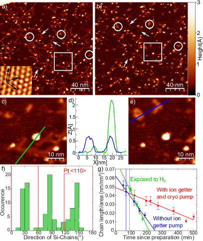
Figure 1(a) shows the STM image of a clean Pt(111) surface, 50 minutes after exposure to 0.03 ML Si. Small clusters about 200 pm in height are visible. In addition, a network of faint lines is apparent (arrows). The lines are 25 pm high and appear few nm in width, as shown in the profile line in Fig. 1(d). Additionally, small extended areas of about 60-70 pm in height are observed (circles and blue profile line in Fig. 1(d)). 140 minutes later, an image of the same area (Fig. 1(b)) reveals that most of the lines have disappeared (white arrows) while some of the 60-70 pm high areas have grown in size (white circles). Figures 1(c) and (e) display enlarged views of the same area (white squares in Figs. 1(a) and (b)) highlighting the disappearance of the network of lines (lower half) and the growth of the more compact areas (upper left corner). About four hours after preparation (corresponding to 300 Langmuir of residual gas exposure) we do not find any of the lines anymore.
The lines exhibit a preferential orientation close to the direction, as shown by the histogram in Fig. 1(f). For the histogram, the angle of the line direction relative to the atomic rows (inset in (a)) was determined by visual inspection. We evaluated several images after three preparation cycles.
We assume that the lines are embedded in the Pt(111) surface for the following reasons. Since we observe different structures induced by the Si deposition, one having the typical height of an atomic step (2 Å), it is rather unlikely that the other structures are also located on top of the Pt(111) surface. Moreover, the lines have the same height as observed for dislocation lines on the Pt(111) surface (25 pm) Bott et al. (1993); Hohage et al. (1995). Hence we argue that the Si is embedded into the Pt(111) surface along the direction. This is supported by the fact that no movement of the lines could be induced by the STM tip up to V=0.3 V and I=9.5 nA. We propose an atomistic model of the embedded Si atoms further below.
The speed at which the lines disappear depends on the amount and composition of the residual gas. Figure 1(g) shows the development of the line lengths per area in different environments. The line length was determined by first flattening the STM images. We applied a \nth3-order plane-fit to remove the slight curvature of the images (caused by piezo creep) and subsequently a conditional line fit, which excludes protruding areas such as Si lines and clusters in order to prevent offsets due to the inhomogeneous distribution of those. Then, the 200 pm high clusters were identified by their protruding height and removed from the image. As the clusters are broadened due to the convolution with the tip, the identified cluster areas were increased by 1 nm in width to also remove the apparent clusters’ rims. The area of the lines was then identified by using the image area exhibiting a height between the half-height of the lines and their full height, which was itself determined by averaging the height of 20 profile lines placed through chains by visual inspection. In order to finally get a length, the resulting area value was divided by the average line width, which is taken as the width of the line perpendicular to the directions. The error of the resulting line length per area is dominated by the error of the determined line height, influencing the area value via the resulting cut-off at half-height.
Under optimized UHV conditions, at , which were obtained when an additional cryo pump is turned on for the final flash during the Pt cleaning and kept running throughout the STM measurement, some lines are still observed 8 hours after Si deposition, i.e, after exposure to 4 Langmuir of residual gas (Fig. 1(g)). Without the ion getter pump operating and without the cryo pump, the pressure is by more than a factor of 100 larger, while the slope of the line length/area vs. time is steeper by only a factor of 3-4 (Fig. 1(g)). Hence, one suspects that only part of the residual gas is responsible for the lifting of the Si lines. Mass spectroscopy reveals that the amount of CHn increases by about three orders of magnitude and the amount of H rises by about one order of magnitude (mainly due to the rise of carbon hydroxides) while the amounts of H2 and CO rise by a factor of about 1.5 only after turning off the ion getter pump. Thus, H2 and carbon monoxide are likely candidates lifting the Si lines. To test this hypothesis, either H2 or CO were deliberately let into the chamber during the STM measurements. In both cases, the samples were prepared while the ion getter pump was operating. After a first STM image to check the success of the preparation, the gas was let in via a dosing valve. An exposure of 40 Langmuir H2 was necessary until the Si lines disappeared completely. This is 10 times more than the dose of residual gas required at the optimal UHV conditions. Hence, while the additional H2 fastens the lifting of the lines, it cannot be solely responsible for their fragility under UHV conditions.
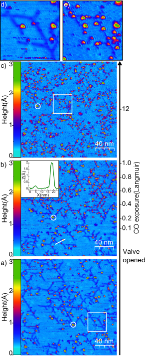
In contrast, about one Langmuir of CO is sufficient to reduce the line density significantly, as can be seen in Fig. 2. Figure 2(a) shows a STM image prior to gas exposure. The contrast is optimized to increase the visibility of the lines showing up in a dark blue color. At the bottom of Fig. 2 (b), which is scanned from bottom to top, CO was let into the chamber. Over the course of that image, the number of lines start to diminish, while additional clusters appear on the surface. Figure 2(c) shows the same area again revealing the nearly complete absence of lines. Hence, CO is much more efficient in lifting the lines than H2. However, the resulting morphology is different than under UHV conditions. Exposed to residual gas, the disappearance of the lines mainly resulted in the growth of small embedded areas with a height of about 60-70 pm, while the exposure to CO results in the growth of small clusters with height of 200 pm along the former lines, while no embedded areas grow. In residual gas these embedded areas did not disappear even after 24 hours and no growth of clusters was observed. Thus, other components of the residual gas might play a role in the exact process of lifting the lines, though CO plays a major role, likely initiating the process.
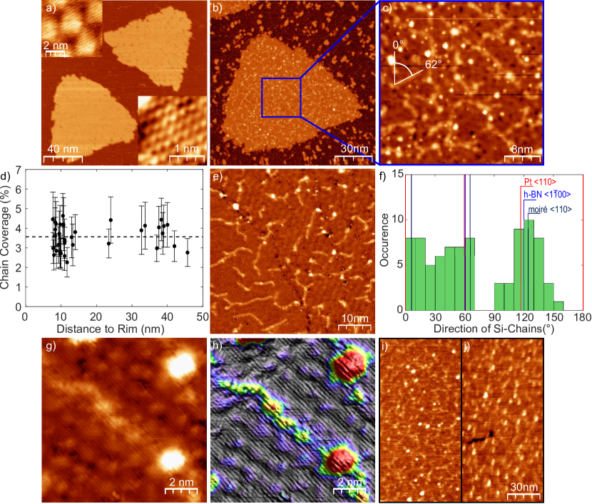
Next, we describe the experiments employing the h-BN protection layer. Figure 3(a) shows Pt(111) exposed to borazine for 10 minutes in order to grow h-BN islands. The h-BN forms mostly triangular islands Farwick zum Hagen et al. (2016). Afterwards the sample was exposed to 0.07 ML of Si at room temperature. A STM image of an h-BN island after exposure to Si is shown in Fig. 3(b). The bare Pt(111) surface surrounding the h-BN island is covered with clusters originating from the Si deposition without any remaining traces of lines. The zoom into the h-BN island in Fig. 3(c), however, shows one dimensional lines with some small clusters in between. No extended areas of sub-monolayer height were observed below h-BN islands.
The first question to be addressed is whether the lines are located below or on top of the h-BN. We argue that they are located below, as supported by the following arguments.
First, the atomic lattice of the h-BN as apparent in STM images continues over the lines and clusters. Figure 3(g) and (h) show the same atomically resolved STM image which includes a Si line in two different representations. The image was processed in the same way as described for Fig.1. No fast Fourier transform (FFT) filter has been applied to the images.The atomic corrugation of the h-BN atoms is only about 2 pm, so it is rather hard to see them in Fig. 3(g) at normal color code representation. Optimizing the contrast in Fig. 3(h), however, clearly reveals the continuation of the atomic rows of the h-BN across the Si lines and clusters. This can only be rationalized if the lines and clusters are below the h-BN layer.
Second, our DFT calculations of a silicene sheet between h-BN and Pt(111) reveal a weak physisorption between Si and h-BN (91 meV per atom), but a stronger chemisorption of the Si to the Pt (1.435 eV). Thus, from an energetical point of view, it is much more favorable for the Si to bind to the Pt, implying that the Si atoms gain energy by moving below the h-BN cover.
Third, no movement of the clusters and lines could be induced by the STM tip down to V=25 mV and up to I=26 nA. Our density functional theory (DFT) calculations of a silicene sheet on h-BN on Pt(111) reveal that the silicene sheet is only physisorbed with an energy gain of 127 meV per atom on the h-BN surface. Consequently, the Si atoms, if only attached to the h-BN, should even be mobile at 300 K, though dangling bonds from the Si clusters, might also prevent their mobility on the h-BN.
Finally, contrary to the lines on the bare Pt(111), the lines below the h-BN are long-term stable in UHV. They are still observed nine days after the preparation and even largely withstand an exposure to air for about 10 minutes corresponding to Langmuir. Figure 3(i) and (j) showcase the sample before and after air exposure. The area surrounding some defects appears darker after the exposure probably due to oxidation, but lines are still observable in the STM image. Considering the instability of the lines on bare Pt(111), this points to an excellent protection below the monolayer of h-BN.
Thus, we conclude that the Si is intercalated between the h-BN and the Pt. By analogy, we assume that the lines being about 25 pm in height are embedded into the Pt(111) surface, while the 200 pm high clusters are located on top of the Pt(111) surface. The driving force for the embedding is likely again the increase of electron density in the Pt(111) surface, which does not profit significantly from the h-BN due to its large band gap of 4.5 eV Bhattacharya et al. (2012).
It is remarkable that Si can be implanted below h-BN from a thermal evaporator. Monolayer h-BN has been shown to protect other intercalated structures. For example, Ar+ and Xe+ ions have been implanted below h-BN layers on metal surfaces forming gas-filled blisters Valerius et al. (2017); Cun et al. (2013, 2014a, 2014b). Trapped Xe+ ions have been observed even after annealing up to 1550 K, at which point the h-BN decomposes freeing the Xe+ Valerius et al. (2017). Ar+-filled blisters survive exposure to air Cun et al. (2014b). However, these structures were created by bombarding the surface with low to high-energy ions, as the expected displacement threshold energies for B and N are 20 eV Kotakoski et al. (2010). The thermal energy provided to the Si atoms is small in comparison.
In order to determine the pathway of Si intercalation, we analyzed the coverage with lines as a function of distance to the rims of the h-BN island using small cut-outs of larger images. The length of the lines per image area was determined with the same routine as used for Fig. 1(g). The Si coverage in percent of a monolayer is given in Fig. 3(d), assuming lines with a width of one Si atom and an inter Si-separation of 2.77 Å (see below). As there is no rise in the coverage closer to the rim, we deduce that the Si does not intercalate from the sides of the island, but diffuses through the h-BN. This might be due to a strong binding of the h-BN edges to the metal due to the open bonds of the h-BN flakes. This is in line with DFT calculations for h-BN on Ir(111) Farwick zum Hagen et al. (2016) revealing a relatively strong binding of the h-BN edges to the metal substrate.
The Si does also not intercalate via grain boundaries as evidenced by Fig. 3(e), showing a fully closed h-BN layer on top of Pt(111) after Si deposition. The image does not show any accumulation of Si lines or clusters along the grain boundary. The lines even simply cross the boundary between the two differently oriented moiré structures, showing that the lines are barely influenced in their growth by grain boundaries of the h-BN.
Next, we also tried to lift the Si lines below the h-BN. We found that a way to lift them is heating to 200∘C, which causes all lines to vanish, while the 200 pm high clusters grow in size (not shown). However, no growth of extended sub-monolayer high areas was observed, so that the mechanism is different to the one observed by exposing the bare Pt surface with Si chains to residual gas. The growth of the islands via the material from the lines can be used to estimate the atomic width of the lines. The coverage with clusters below the h-BN before heating was determined to be by flooding the image above the half-height of the clusters. The error was determined from varying the flooding limit in the range of the error on the visually determined cluster height. After heating to 200∘C, the clusters cover of the surface below the h-BN. The difference of corresponds nicely to the coverage of Si atoms in the lines of prior to annealing (Fig. 3(d)), if one assumes a width of one atom and an inter-Si-distance equal to the Pt-Pt distance in the Pt(111) surface. In turn, division of these two values gives a line width of atoms. Thus, the embedded lines below the h-BN appear to be atomically thin one-dimensional Si chains. Such an estimate of the width could not be realized on the bare Pt(111) as we were not able to deduce a clear atomic model for the more compact, embedded areas (likely a precursor of the surface silicide Švec et al. (2014)). Thus, we could not estimate the amount of atoms contained within them.
While the line network below the h-BN exhibits similarities to the one on bare Pt(111), there is one striking difference. While on bare Pt the lines are oriented preferentially along the -direction, beneath the h-BN they are preferentially orientated along the three -directions. Figure 3(f) shows a histogram of the angle of the lines with respect to the atomic rows (inset in Fig.1(a)). While it exhibits more variations than Fig. 1(f), in line with the stronger meandering of the lines in Fig. 3 than in Fig. 1, its maxima are along the directions, distinct from the case on the bare Pt(111). This will be tentatively explained by the influence of the strain within the h-BN layer.
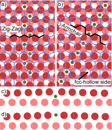
We, thus now provide tentative atomic models (Fig. 4) that might be the starting point to explain our intriguing experimental observations in detail. As discussed in the introduction, a Pt surface gains energy by incorporating further atoms. For platinum silicides, whose bare existence testifies to the solubility of Si in Pt, different bonding configurations are found. They range from more covalent Pt2Si to more metallic PtSi Klepeis et al. (2001). One has also observed an embedding of the silicon in the top layer at intermediate temperature Švec et al. (2014), which is dubbed a surface Pt silicide.
The atomic configuration of the bare Pt(111) surface offers most space for embedment in the hollow-site, fcc-type positions (Fig. 4(b)). We propose that the silicon atoms are located there. Depending on the position of the next nearest Si neighbors, the result is a chain in or -direction. The resulting structures, with the known Si density (discussion above) are shown in Figs. 4(a) and (b). In these structures, neighboring Si atoms have a distance of 277 pm. This is much larger than in any bonding configuration of pure silicon, so one can assume that the chains are not the result of Si-Si interactions, but rather governed by the Si-Pt interactions. Assuming additionally that the main driving force for the Si embedment is the increase of electron density in the Pt surface Bott et al. (1993); Hohage et al. (1995); Sandy et al. (1992); Lundgren et al. (1999); Grütter and Dürig (1994); Holst et al. (1998); Zhang et al. (1999), Si atoms should be placed at positions that barely dusturb the Pt lattice. Two such positions, depicting the ionic radius of the different atoms via its symbol size, are shown in Figs. 4(c) and (d). Either the Si atom is located in the surface (Fig. 4(d)), as observed for the surface Pt silicide Švec et al. (2014), or it is in the largest empty space in between the two top layers of Pt(111) (Fig. 4 (c)), where the Si atom would be six-fold coordinated similar to PtSi Klepeis et al. (2001). Without further calculations, we cannot decide which position is more favorable for the embedded Si chains.
However, we want to provide a model idea, why the orientation of the chains on bare Pt(111) and on h-BN covered Pt(111) is different. Inspecting the two different chain directions with h-BN on top (Figs. 4 (a),(b)), one notices that one configuration stretches the h-BN along the zig-zag-direction, while the other one stretches it along the armchair-direction (black lines of the h-BN lattice). Classical molecular dynamics calculations (employing finite-size h-BN layers) indeed show a difference in the Young’s modulus for different stretching directions Thomas et al. (2016, 2017). Specifically, is smaller in the armchair-direction (755 GPa at 300 K) than in the zig-zag direction (769 GPa at 300 K). This might lead the chains to be preferentially orientated perpendicular to the armchair direction, when there is a h-BN layer on top.
While it remains unclear, why the chains are orientated along the Pt--directions without h-BN on top, we notice that dislocation lines in the bare Pt(111) surface induced by excess Pt or Co are orientated along that axis, too Bott et al. (1993); Hohage et al. (1995); Sandy et al. (1992); Lundgren et al. (1999); Grütter and Dürig (1994); Holst et al. (1998); Zhang et al. (1999).
V Conclusion
In conclusion, we have demonstrated that Si deposition onto Pt(111) at 300 K forms a network of atomically thin 1D Si chains embedded into the Pt(111) surface. The chains disappear in UHV within hours due to residual gas adsorption, most importantly by CO. The chain network can be protected by a monolayer of h-BN, covering the Pt(111) surface before deposition of the silicon. This makes the chains stable for weeks in UHV and even stable in air for, at least, 10 min. The h-BN coverage, additionally, results in a rotation of the chains by 30∘, likely due to the anisotropic mechanical properties of h-BN.
The largely airtight protection of the one atom thick Si structures by a h-BN monolayer underlines the potential of 2D materials for protection of fragile heterogeneous atomic assemblies. This might be exploited for other self-organized structures, too.
Acknowledgements.
We thank B.Voigtländer (FZ Jülich) for providing us with a Si evaporator Mysliveček et al. (2002) and A. Grüneis (Univ. of Cologne) for help regarding the handling of borazine. Most of the STM data was analyzed using the WSxM software Horcas et al. (2007). In particular, the ”Flatten plus”-function proved extremely useful. Funding by the Graphene Flagship (Contract No. 696656) and the Excellence Initiative of the German federal and state governments is gratefully acknowledged. P. Nemes-Incze acknowledges support form the Hungarian Academy of Sciences, within the framework of the MTA EK Lendület Topology in Nanomaterials Research Group, grant no: LP2017-9/2017. The computations were performed at the high-performance computer JURECA operated by the JSC at the Forschungszentrum Jülich. V. Caciuc and N. Atodiresei acknowledge financial support from the DFG through the Collaborative Research Center SFB 1238 (Project No. C01).References
- Zangwill (1988) A. Zangwill, Physics at Surfaces (Cambridge University Press, 1988).
- Barth et al. (1990) J. V. Barth, H. Brune, G. Ertl, and R. J. Behm, Phys. Rev. B 42, 9307 (1990).
- Bott et al. (1993) M. Bott, M. Hohage, T. Michely, and G. Comsa, Phys. Rev. Lett. 70, 1489 (1993).
- Hohage et al. (1995) M. Hohage, T. Michely, and G. Comsa, Surf. Sci. 337, 249 (1995).
- Sandy et al. (1992) A. R. Sandy, S. G. J. Mochrie, D. M. Zehner, G. Grübel, K. G. Huang, and D. Gibbs, Phys. Rev. Lett. 68, 2192 (1992).
- Lundgren et al. (1999) E. Lundgren, B. Stanka, W. Koprolin, M. Schmid, and P. Varga, Surf. Sci. 423, 357 (1999).
- Grütter and Dürig (1994) P. Grütter and U. T. Dürig, Phys. Rev. B 49, 2021 (1994).
- Holst et al. (1998) B. Holst, M. Nohlen, K. Wandelt, and W. Allison, Phys. Rev. B 58, R10195 (1998).
- Zhang et al. (1999) L. P. Zhang, J. van Ek, and U. Diebold, Phys. Rev. B 59, 5837 (1999).
- Michely (1996) T. Michely, Atomare Prozesse bei der Pt-Abscheidung auf Pt(111) (Rheinische Friedrich-Wilhelms-Universität Bonn, 1996) pp. 116–127.
- Tempas et al. (2016) C. D. Tempas, D. Skomski, and S. L. Tait, Surf. Sci. 654, 33 (2016).
- Barth et al. (1996) J. Barth, R. Schuster, R. Behm, and G. Ertl, Surf. Sci. 348, 280 (1996).
- Anic et al. (2016) K. Anic, A. Bukhtiyarov, H. Li, C. Rameshan, and G. Rupprechter, J. Phys. Chem. C 120, 10838 (2016).
- Geringer et al. (2009) V. Geringer, M. Liebmann, T. Echtermeyer, S. Runte, M. Schmidt, R. Rückamp, M. C. Lemme, and M. Morgenstern, Phys. Rev. Lett. 102, 076102 (2009).
- Musket et al. (1982) R. Musket, W. McLean, C. Colmenares, D. Makowiecki, and W. Siekhaus, Appl. Surf. Sci. 10, 143 (1982).
- Morgenstern et al. (1997) M. Morgenstern, T. Michely, and G. Comsa, Phys. Rev. Lett. 79, 1305 (1997).
- Ćavar et al. (2008) E. Ćavar, R. Westerström, A. Mikkelsen, E. Lundgren, A. Vinogradov, M. L. Ng, A. Preobrajenski, A. Zakharov, and N. Mårtensson, Surf. Sci. 602, 1722 (2008).
- Preobrajenski et al. (2007a) A. Preobrajenski, M. Nesterov, M. L. Ng, A. Vinogradov, and N. Mårtensson, Chem. Phys. Lett. 446, 119 (2007a).
- Preobrajenski et al. (2007b) A. B. Preobrajenski, A. S. Vinogradov, M. L. Ng, E. Ćavar, R. Westerström, A. Mikkelsen, E. Lundgren, and N. Mårtensson, Phys. Rev. B 75, 245412 (2007b).
- Mysliveček et al. (2002) J. Mysliveček, C. Schelling, F. Schäffler, G. Springholz, P. Šmilauer, J. Krug, and B. Voigtländer, Surf. Sci. 520, 193 (2002).
- Vogt et al. (2012) P. Vogt, P. De Padova, C. Quaresima, J. Avila, E. Frantzeskakis, M. C. Asensio, A. Resta, B. Ealet, and G. Le Lay, Phys. Rev. Lett. 108, 155501 (2012).
- Jamgotchian et al. (2012) H. Jamgotchian, Y. Colignon, N. Hamzaoui, B. Ealet, J. Y. Hoarau, B. Aufray, and J. P. Bibérian, J. Phys. Condens. Matter 24, 172001 (2012).
- Lucier et al. (2005) A.-S. Lucier, H. Mortensen, Y. Sun, and P. Grütter, Phys. Rev. B 72, 235420 (2005).
- Hohenberg and Kohn (1964) P. Hohenberg and W. Kohn, Phys. Rev. 136, B864 (1964).
- Kohn and Sham (1965) W. Kohn and L. J. Sham, Phys. Rev. 140, A1133 (1965).
- Blöchl (1994) P. E. Blöchl, Phys. Rev. B 50, 17953 (1994).
- Kresse and Hafner (1993) G. Kresse and J. Hafner, Phys. Rev. B 47, 558 (1993).
- Kresse and Furthmüller (1996) G. Kresse and J. Furthmüller, Phys. Rev. B 54, 11169 (1996).
- Kresse and Joubert (1999) G. Kresse and D. Joubert, Phys. Rev. B 59, 1758 (1999).
- Lee et al. (2010) K. Lee, E. D. Murray, L. Kong, B. I. Lundqvist, and D. C. Langreth, Phys. Rev. B 82, 081101 (2010).
- Hamada (2014) I. Hamada, Phys. Rev. B 89, 121103 (2014).
- Becke (1986) A. D. Becke, The Journal of Chemical Physics 85, 7184 (1986).
- Farwick zum Hagen et al. (2016) F. H. Farwick zum Hagen, D. M. Zimmermann, C. C. Silva, C. Schlueter, N. Atodiresei, W. Jolie, A. J. Martínez-Galera, D. Dombrowski, U. A. Schröder, M. Will, P. Lazić, V. Caciuc, S. Blügel, T.-L. Lee, T. Michely, and C. Busse, ACS Nano 10, 11012 (2016).
- Bhattacharya et al. (2012) A. Bhattacharya, S. Bhattacharya, and G. P. Das, Phys. Rev. B 85, 035415 (2012).
- Valerius et al. (2017) P. Valerius, C. Herbig, M. Will, M. A. Arman, J. Knudsen, V. Caciuc, N. Atodiresei, and T. Michely, Phys. Rev. B 96, 235410 (2017).
- Cun et al. (2013) H. Cun, M. Iannuzzi, A. Hemmi, S. Roth, J. Osterwalder, and T. Greber, Nano Letters 13, 2098 (2013).
- Cun et al. (2014a) H. Cun, M. Iannuzzi, A. Hemmi, J. Osterwalder, and T. Greber, ACS Nano 8, 1014 (2014a).
- Cun et al. (2014b) H. Cun, M. Iannuzzi, A. Hemmi, J. Osterwalder, and T. Greber, ACS Nano 8, 7423 (2014b).
- Kotakoski et al. (2010) J. Kotakoski, C. H. Jin, O. Lehtinen, K. Suenaga, and A. V. Krasheninnikov, Phys. Rev. B 82, 113404 (2010).
- Švec et al. (2014) M. Švec, P. Hapala, M. Ondráček, P. Merino, M. Blanco-Rey, P. Mutombo, M. Vondráček, Y. Polyak, V. Cháb, J. A. Martín Gago, and P. Jelínek, Phys. Rev. B 89, 201412 (2014).
- Shannon (1976) R. D. Shannon, Acta Cryst. A 32, 751 (1976).
- Klepeis et al. (2001) J. E. Klepeis, O. Beckstein, O. Pankratov, and G. L. W. Hart, Phys. Rev. B 64, 155110 (2001).
- Thomas et al. (2016) S. Thomas, K. M. Ajith, and M. C. Valsakumar, J. Phys. Condens. Matter 28, 295302 (2016).
- Thomas et al. (2017) S. Thomas, K. M. Ajith, and M. C. Valsakumar, Mat. Res. Express 4, 065005 (2017).
- Horcas et al. (2007) I. Horcas, R. Fernández, J. M. Gómez-Rodriguez, J. Colchero, J. Gómez-Herrero, and A. M. Baro, Rev. Sci. Instrum. 78, 013705 (2007).